Note: Descriptions are shown in the official language in which they were submitted.
CA 02290370 1999-11-17
WO 98/57380 PCT/US98/12130
Annealing of a Crystalline Perovskite Ferroelectric Cell
and Cells Exhibiting Improved Barrier Properties
FIELD OF THE INVENTION
The invention generally relates to ferroelectric structures integrated onto
substrates
such as silicon. In particular, the invention relates to the fabrication
process of producing a
crystallographically oriented ferroelectric structure.
io
BACKGROUND ART
Considerable interest exists in fabricating integrated circuit (IC) memories
which are
non-volatile, that is, ones that continue to store data after the IC chip has
been powered down.
One type that is reaching the market is a ferroelectric memory in which the
gap between the
is capacitors of an electrode is filled with a ferroelectric material which
can be electrically poled
into two stable states. The commercial activity to date has involved
polycrystalline
ferroelectric materials. Despite intensive developmental efforts, these
polycrystalline
ferroelectric IC memories exhibit poor fatigue.characteristics and suffer from
tow yield in
manufacture.
2 o In an alternative approach under development, the ferroelectric material
is grown in a
crystailographically oriented phase. It is believed that under the proper
conditions the
ferroelectric grows in a columnar multicrystalline structure with the <001>
axis of the layered
perovskite crystal structure of typical ferroelectrics being preferentially
oriented normal to the
ferroelectric film. Examples of the ferroelectric materials include lead
zirconium titanate
2 s (PZT), lead laathanum zirconium titanate (PLZT), lead niobium zirconium
titanate (PNZT).
Columnar crystallites are formed with random orientation within the plane of
the film.
Dhote and Ramesh, two of the present inventors, have disclosed two distinct
but
related structures in U.S. Patent Applications, Serial No. 08/578,499 filed
December 26, 1995
and Serial No. 08/582,545 filed January 3, 1996, both incorporated herein by
reference in their
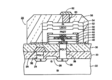
3 o entireties. The structure of the latter patent application is illustrated
in the cross-sectional
view of FIG. 1. An illustrated ferroelectric random access memory (IrRAIV~
cell 20, of which
i
CA 02290370 1999-11-17
WO 98/57380 PCT/US98/12130
many are formed in the IC memory, is formed on a <001>-oriented crystalline
silicon substrate
22 and includes both a ferroelectric capacitor and a transistor. A metal-oxide-
semiconductor
(MOS) transistor is created by forming source and drain wells 24, 26 having a
conductivity
type opposite to that of the substrate 22. The intervening gate region is
overlaid with a gate
structure 28 including a lower gate oxide and an upper metal gate line, for
example of
aluminum, to control the gate.
A first inter-level dielectric layer 30 is deposited over the substrate and
the transistor
structure. A through hole 32 is etched through the first inter-level
dielectric layer 30 in the
area over the source well 24, and polysilicon is filled into the through hole
32 to form a
io polysilicon contact plug to the transistor source. A metal source line 34
is
photoiithographically delineated on top of the first inter-level dielectric
layer 30 and
electrically contacts the polysilicon plug 32.
A second inter-level dielectric layer 36 is then deposited over the first
inter-level
dielectric layer 30. Another through hole 38 is etched through both the first
and second inter-.
15 level dielectric layers 30, 36 over the area of the drain well 26, and
polysilicon is filled into the
second through hole 38 to form a contact plug to the transistor drain.
A lower ferroelectric stack is then deposited and defined. It includes a
polysilicon
layer 40 to promote electrical contact to the polysilicon plug 38, a titanium
nitride (TiN) layer
42 acting as a first conductive barrier between the underlying polysilicon and
the oxidizing
2 o ferroelectric Iayer and its oxide electrodes, an intermetallic layer 44
acting as the primary
barrier, and a lower metal-oxide electrode 46.
Growth of the metal-oxide electrodes 46, 52 and the ferroelectric layer 50 is
performed
at temperatures in the range of 500° to 650°C, the highest
temperatures achieved in the
processing after the deposition of the intermetallic layer 44.
2 s The intermeiallic layer 44 is novel to the cited patent application. It
may have a
composition of Ti3Al, among other possibilities to be discussed later. In
brief, an intermetallic
is an alloy of at least two metals, one of which is refractory, and the metals
are combined in
stoichiometric or near stoichiometric ratios. There results a metal with long-
range atomic
order, that is, a metal that is at least polycrystalline. Liu et al. provide a
good introduction to
3 o intermetallics, at least as used for mechanical components, in "Ordered
Intermetallics," ASM
CA 02290370 1999-11-17
WO 98/57380 PCT/US98/12130
Handbook, vol. 2, Properties and Selection: Nonferrous Alloys and Special-
Purpose
Materials (ASM International, 1992) pp. 913-942).
The lower metal-oxide electrode may have a composition of lanthanum strontium
cobaltite (LSCO), and in particular a composition of approximately
La,.xSrxCo03, where
s 0.15'x30.85. It is now well known that LSCO forms an acceptable electrical
contact and
futher promotes highly oriented growth of perovskite ferroelectric materials.
Several
variations on the structure of the lower ferroelectric stack are possible.
Neither the polysilicon
layer 40 nor the TiN layer 42 is considered crucial, and either or both may be
dispensed with.
A Z-shaped field-oxide layer 48 is formed around the sides of the lower
ferroelectric
1o stack and extends over its rim and laterally outwards from its bottom but
leaves a central
aperture for the after deposited upper ferroelectric stack.
The upper ferroelectric stack is then deposited and defined to fill the
aperture of the
field oxide layer 48 but not to extend beyond the end of its foot. The upper
ferroelectric stack
includes the ferroelectric layer 50, for example of PNZT, the upper metal-
oxide electrode layer
i5 52, for example of LSCO, and a platinum layer 54.
A third inter-layer dielectric layer 56 is deposited around the upper and
lower
ferroelectric stacks. A via hole 60 is etched down to the platinum layer 54,
and TiJW is filled
into the hole to form a via 60 contacting the platinum layer 54. An aluminum
layer is
deposited and delineated to form an interconnect line 62 connected to the via
60.
2 o Prototype ferroelectric capacitor stacks have been grown following the
vertical stack
structure shown in FTG. 1. Both the LSCO electrodes 4b, 52 and the
ferroelectric layer 50
have been shown to exhibit highly crystalline orientation. The fetroelectric
stacks were
measured to have polarization, fatigue, and retention properties superior to
those available
from polycrystalline ferroelectric cells.
2 s Nonetheless, the results still need improvement. The cell manufactured
according to
the process euhibits a hysteresis curve adequate for operation at SV. However,
for high-level
integration, 3V operation is greatly desired. The polarizability of the
ferroelectric cell needs to
be improved for 3 V operation.
3
CA 02290370 1999-11-17
WO 98/57380 PCT/US98/12130
SUMMARY OF THE INVENTION
The invention can be summarized as a method of fabricating a perovsitite layer
over a
metal-oxide layer. At least the metal-oxide layer is subjected to a rapid
thermal anneal after its
deposition.
A ferroelectric memory cell is formed over a silicon substrate with an
intermediate
intermetallic layer. A ferroelectric cell is formed by the sequential growth
of a lower metal-
oxide electrode, a ferroelectric layer, and an upper metal-oxide layer. At
least the lower
metal-oxide electrode is annealed for a relatively short time at a temperature
above the
temperature at which it was grown.
1o In another aspect of the invention, the intermetallic layer is formed of a
silicide, most
preferably a disilicide of a refractory metal.
In~yet another aspect of the invention, a second intermetallic layer is formed
over the
upper metal-oxide layer to provide electrical contacting to an upper metal
level. The second
intermetallic layer eliminates the need for platinum on the upper side. More
preferably, the
second intermetallic layer is formed of an intermetallic aluminide to provide
a robust interface
to an aluminum interconnect plug and aluminum wiring.
BRIEF DESCRIPTION OF THE DRAWINGS
FIG. 1 is a cross-sectional view of a ferroelectric memory cell utilizing an
intermetallic
2 o barrier.
FIG. 2 is a cross-sectional view of a test structure used as a prototype for
the memory
cell of FIG. 1.
FIG. 3 is a graph showing a series of hysteresis curves for a ferroelectric
capacitor of
the invention.
2 s FIG. 4 is a graph comparing the remanent polarization of a ferroelectric
capacitor with
and without the annealing of the invention.
FIG. 5 is a graph showing polarization properties of a ferroelectric capacitor
of the
invention.
FIG. 6 is a graph of the fatigue characteristics at two different temperatures
for
3 o ferroelectric capacitors of the invention.
4
CA 02290370 1999-11-17
WO 98/57380 PCT/US98/12130
FIG. 7 is a graph of the fatigue characteristics of ferroelectric capacitors
with and
without the annealing of the invention.
FIG. 8 is a graph of the dependence of remanent polarization upon the amount
of
annealing of the invention.
s FIG. 9 is a graph of the dependences of remanent polarization and surface
resistivity
upon the amount of annealing of the invention.
FIG. 10 is a graph of polarization properties of ferroelectric capacitors
lacking a
titanium nitride barrier and alternately being annealed and not annealed.
FIG. 11 is a graph of fatigue characteristics for the fetTOelectric capacitors
of FIG. 10.
to FIG. 12 is a cross-sectional view of an alternative embodiment of the
memory cell of
the invention having an intermetallic upper contact layer.
FIr. 13 is a graph of the hysteresis curves for two cells alternatively using
an
intermetallic and a platinum upper contact layer.
FIG. 14 is a cross-sectional view of a ferroelectric memory cell utilizing a
silicide
i5 barrier.
FIG. 15 is a graph showing two hysteresis curves for a test structure with a
silicide
barrier.
DETAILED DESCRIPTION OF THE PREFERRED EMBODIIvviENTS
2 o In one embodiment of the invention, the structure of FIG. 1 is fabricated
by much the
same techniques as are described in the referenced patent application, as has
been briefly
described. As in the previously described growth of the lower ferroelectric
stack, the lower
metal-oxide electrode layer 46 is grown in the temperature range of 550 to
650°C and cooled
in an oxygen-rich environment. However, thereafter, the substrate is removed
from the
2 5 growth chamber aad is subjected to a rapid thermal anneal at a temperature
above its growth
temperature for a relatively short period of time. Following the anneal, the
previously
described processing is resumed, and the structure is completed. By means of
the rapid
thermal anneal, the polarization characteristics of the fetroelectric
capacitor are improved
while the fatigue and retention characteristics are at least maintained.
3 o It is believed that the rapid thermal anneal causes the columnar
crystallites in the lower
metal-oxide layer 46 to enlarge to larger diameters. This layer 46 acts as a
crystalline growth
s
CA 02290370 1999-11-17
WO 98/57380 PCT/US98/12130
template for the growth of the overlying ferroelectric Iayer 50 with a highly
oriented crystalline
structure. Since the underlying metal-oxide template layer 46 has large
crystallite sizes after
the rapid thermal anneal, the after grown ferroelectric layer 50 also has
larger crystallite sizes.
Ferroelectric domains are known to have diameters of tens of nanometers. If
the diameters of
s the columnar crystallites are several times this value, then each
crystallite will contain several
domains. That is. not all ferroelectric domains will extend across grain
boundaries. Hence,
grain boundaries and any subsequent diffusion along the grain boundaries will
not affect all the
ferroelectric domains, and the columnar ferroelectric layer will more resemble
a singly
crystalline layer.
io A second effect is that the rapid thermal anneal will remove defects from
the surface
and the bulk of the lower metal-oxide layer 46 that would degrade the
subsequent growth and
would also affect the electrical characteristics of that interface. For
example, in an oxygen-
rich anneal, the perovskites can absorb more oxygen and reduce the
concentration of oxygen
vacancies. In some situations, the anneal amounts to a crystallization of a
generally
is amorphous deposited layer.
A large number of experiments were performed on prototype structures to
confirm the
advantages of the invention. Unpatterned ferroelectric stacks were grown on
either silicon
wafers covered by a polysilicon layer or silicon wafers covered by polysilicon
and then
titanium nitride. The growths were performed by pulsed laser deposition (PLD)
with a KrF
2 o excimer laser pulsed at 5Hz at a fluence per pulse of 3Jxcrri Z. The
growths were performed
with the subsuate holder held at 600°C. The intermetallic layer 42 was
deposited in a high
vacuum while the metal-oxide and ferroelectric layers were deposited in an
oxygen ambient of
100mTorr. The metal-oxide layers 46, 52 had compositions of Lao,sSro_SCo03
(LSCO) and
thicknesses of 100nm. The ferroelectric layer 50 had a composition of
PbNbfl.~eZro.28Tio.6g03
z s (PNZT) and a thickness of 300nm. Most of the samples included the top
platinum layer 54.
Most electrical characterizations were performed upon a prototype capacitor
swcture
shown in FIG. 2. A base structure includes a crystalline silicon substrate 70,
a polysilicon
layer 72, and a TiN layer 74. A platinum contact 75 is applied to an exposed
area of the TiN
layer 74. A lower ferroelectric stack includes an intermetallic layer 76, a
lower metal-oxide
3 o electrode layer 78 of LSCO, and a ferroelectric layer 82 of PNZT. An upper
metal-oxide
electrode layer 84 is deposited over the ferroelectric layer 82 and formed
into relatively small
CA 02290370 1999-11-17
WO 98/57380 PCT/US98/12130
memory capacitors 88 and a much larger coupling capacitor 90. Platinum
contacts 92, 94 are
deposited on the memory and coupling capacitors 88, 90 prior to the capacitor
definition and
defined with them. The individual memory capacitors 88 are electrically
accessed between
their respective contacts 88 and either the coupling capacitor 90 at the top
or the TiN contact
s 75 at the bottom. Details of the fabrication process are found in the latter
referenced patent
application to Dhote and Ramesh.
Experiment 1
A first test chip was fabricated with the intermetallic layer 76 being
composed of
Ni3Al. All the laser ablated oxide layers were deposited at 600°C.
After the deposition of the
io lower LSCO layer 78, the chip was removed from the laser deposition chamber
and subjected
to rapid thermal annealing at 750°C for 120s. The hysteresis loops for
this chip, illustrated in
the graph of FIG. 3, were measured at 100°C. The loops were measured
for different values
of maximum applied voltage, with the largest maximum voltages applied first.
All the loops
manifest good hysteresis> even the 2-volt loop. As ferroelectric memory ICs
are extended to
~s capacities of 256Mb and beyond, operation at lower voltages becomes highly
desirable.
Experiment 2
Two chips were prepared with the intermetallic layer 76 being composed of
AlTi3 with
5wt% doping of Nb. They were grown at room temperature. A comparative chip was
fabricated without the rapid thermal anneal. Its polarization characteristic,
as measured by the
2 o difference between switched and unswitched polarization, is plotted as a
function of applied
voltage in curve 104 in FIG. 4. The pulse width of the poling voltage was 2ms.
Another chip
was subjected to rapid thermal annealing at 750°C for 160s after the
growth of its tower
LSCO layer 78. Its corresponding polarization characteristic is shown in curve
106. The chip
that was annealed showed significantly better polarization, and its
characteristics in the poling
2 s range of 2-3V were acceptable and even better than those of the unannealed
chip at
significantly higher poling voltages.
CA 02290370 1999-11-17
WO 98/57380 PCT/US98/1z130
Experiment 3
Another chip was grown at 600°C with its intermetallic layer of Ni3Al
and was
subjected to rapid thermal annealing. Its remanent polarization ~P and
coercive voltage E
were measured as a function of the applied voltage. The remanent polarization
is difference
between the switched and unswitched polarizations and the coercive voltage is
the voltage
value shown in the hysteresis loop with the polarization is zero. Curve 110 in
FIG. S shows
the remanent polarization; curve 112 shows the coercive voltage. The curves
show that
capacitors grown by this technique have su~cient (remanent) polarization qP at
coercive
voltages E~ of one volt or less for an applied voltage of 3V, a desirable
operating range for
io ULSI memories. As was shown by the data of FIG. 4, an unannealed capacitor
does not
afford such high polarization values.
The capacitors of the data of FIG. 5 were tested for fatigue by applying a
bipolar
square pulse of t5V at IMHz. Curves 120, 122 of FIG. 6 show the remanent
polarization qP
as a function of the number of fatigue cycles while the sample was held at
room temperature.
Curves 124, 126 similarly show the remanent polarization ~P while the sample
was held at
100°C during the fatiguing cycles. It is believed that the improvement
in the remanent
polarization qP after fatiguing at 100°C arises from an effective self-
annealing during cycling at
elevated temperatures. It is noted that the 109 cycles at which the
improvement is nearly
complete at 100°C corresponds to a self annealing time of 17 minutes
but that the self-
2 o annealing was performed after the complete ferroelectric stack had been
grown.
Experiment 4
Both an inventive and a comparative sample were grown at 600°C with an
intermetallic
layer of AlTi3 plus Nb dopants. Fatiguing tests at room temperature were
performed on the
resultant capacitors. Curves 130, 132 of FIG. 7 show the remanent polarization
qP when
2 5 rapid thermal annealing of the bottom LSCO layer was performed at
750°C for 160s while
curves 134, 136 show the remanent polarization qP when no rapid thermal
annealing as
described above was performed. Although the polarization for the annealed
sample does fall
off above about 109 cycles, it still remains above the polarization for the
unannealed sample.
a
CA 02290370 1999-11-17
WO 98/57380 PCT/US98/12130
Experiment .i
Retention time was determined on a sample with an intermetallic layer of Ni,AI
and
which was subjected to rapid thermal annealing. The remanent polarization was
measured as a
fimction of time over a period of about a day. The polarization decreased
approximately with
s the logarithm of the time. If this dependence is assumed to extend to a
polarization of
2mGcm', the retention time at room temperature is about 160,000 years and that
at 100°C is
about 8000 years. These retention times are considered quite adequate.
Experiment b
Several tests were performed to determine the effect of different amounts of
rapid
to thermal annealing. A first set of samples were grown with an intermetallic
layer of AlTi3 with
Nb doping. The lower LSCO layer was deposited at room temperature so that it
was
amorphous or polycrystalline. The samples were then subjected to rapid thermal
annealing at
750°C for times between 80 and 160 seconds. The capacitor fabrication
was thereafter
completed, and the remanent polarization qP was measured on each sample. The
results
i5 generally follow plot 140 in FIG. 8. The initial conclusion is that more
annealing is beneficial.
However, it is believed that excessive annealing will eventually affect the
intermetailic layer
and cause reliability problems. It is generally accepted that the thermal
budget should be
minimized consistent with other requirements. That is, the annealing time and
temperature
should be limited to values required for operational parameters.
2 o A second set of samples were grown with an intermetallic layer of Ni3Al.
After the
growth of the amorphous lower LSCO layer, the samples were subjected to
different amounts
of rapid thermal annealing at 750°C. After completion of the capacitor
structures, both the
remanent polarization and the resistiviry were measured. The resistivity was
measured with a
two-point probe method using one small contact 88 and the large contact 90 of
the type
2 s illustrated in FIG. 2. The measured resistance was normalized to
resistiviry assuming a
capacitor stack of 50mm on a side and a ferroelectric thickness of 300nm. The
experimental
results are shown in curve 142 of FIG. 9 for the rernanent polarization qP and
in curve 144 for
the resistiviry. Similarly to the results of FIG. 8, prolonged rapid thermal
annealing increases
" the polarization. For lesser amounts of annealing, the lower LSCO layer
remained
3 o crystallographicaily unoriented producing a disordered ferroeiectric
layer. The resistiviry is
9
CA 02290370 1999-11-17
WO 98/57380 PCT/US98/12130
nearly constant and confirms that the thickness of the ferroelectric layer did
not significantly
vary between the samples.
The upper bounds of thermal annealing are not easily quantifiable and will
need to be
optimized in an overall process. Rapid thermal annealing of crystalline layers
for more than ~
minutes defeats the purpose of RTA. However, an amorphous LSCO layer could
benefit from
a long anneal, about 15 minutes, in an oxygen-rich environment.
Experiment 7
In our prior patent, we have suggested that a TiN barrier layer is not
required to
separate the intermetallic barrier layer from the underlying silicon. Samples
were grown to
i o confirm this result, both with and without rapid thermal annealing.
Referring to FIG. 2, the
intermetallic layer 76 of Ni3A1 was grown directly on the polysilicon layer
72. The annealing,
if perfortried, was for 120s at 750°C. Curve 150 in FIG. 10 shows the
measured remanent
polarization qP as a function of the applied voltage when the sample was
subject to rapid
thermal annealing while curve 152 shows the corresponding values without
annealing. Curves-
ls 154, 156 show the measured coercive voltage E~ as a function of the applied
voltage for the
annealed and unannealed samples respectively. In comparison with the data
presented in
FIG. 5 for a structure including the TiN barrier layer, it is seen from FIG.
10 that the absence
of the TiN barrier has little effect upon the annealed sample. However, the
rapid thermal
annealing of the non-TiN samples significantly improves the polarization.
2 o Fatigue tests were also performed on these samples. Curves 160, 162 in
FIG. 11 show
the dependence of the remanent polarization upon the number of cycles at
100°C for an
annealed sample while curves 164, 166 show the corresponding dependence for an
unannealed
sample. Similar results are obtained for fatiguing at room temperature
although then the
unannealed sample is not so greatly inferior to the annealed sample. The
results of FIG. 11 for
2 s no TiN barrier should be compared with those of FIG. 6 for a TiN barrier.
All these results
confirm that the intermetallic barrier eliminates the need for a TiN barrier.
The memory cell structure shown in FIG. 1 has some potential problems.
Platinum is
very porous to oxygen so that the upper platinum electrode 54 presents no
barrier to oxygen
diffusing upwardly from the upper metal-oxide electrode 54 to the aluminum in
the plug 60 or
3 o interconnect 62. Oxygen in sufficient amounts causes aluminum to ball up,
introducing
excessive contact resistance and greatly degrading the hysteresis
characteristics observable
io
CA 02290370 1999-11-17
WO 98/57380 PCT/US98/12130
from outside the ferroelectric stack. If the plug 60 is composed of aluminum,
a TiN barrier
may be deposited at the bottom of the contact hole before the aluminum
deposition to prevent
the oxygen diffusion. However, TiN does not adhere well to platinum so an
intermediate glue
layer of TiW may be required. The result is a complex fabrication process.
Alternatively, the
s entire plug 60 may be composed of TiW, but deposition of thick layers of TiW
is not widely
practiced in silicon processing. Furthermore, the platinum is difficult to
etch, particularly in a
production-worthy process.
According to another aspect of the invention, the upper platinum layer 54 of
FIG. 2 is
replaced, as illustrated in FIG. 12, by an upper intermetallic layer 170
directly overlying the
~o upper metal-oxide layer 52. The upper intermetallic layer 170 acts as a
barrier preventing the
upwards migration of oxygen from the metal-oxide layer 52 to the overlying
aluminum.
Advantageously, the upper intermetallic layer 170 is composed of an aluminide
intermetallic,
such as AlTi3, Ni3Al, or NiAI. Then the via hole can be filled with a plug 172
of aluminum,
which will bond well to the underlying aluminide intermetallic layer 170. The
aluminide
i5 provides a good mechanical and ohmic interface between aluminum and the
aluminide
intermetallic. The use of non-aiuminide intermetallics may necessitate a glue
layer between the
aluminum plug 172 and the intermetallic layer 170. As is well known in silicon
processing, the
aluminum of the plug 172 and of the interconnect 62 can be deposited in one
step.
Alternatively, an intermetallic can be filled into the plug 172 and even used
as the interconnect
zo 62. With a change in the geometry of the structure, it is possible to
deposit the plug material
directly onto the upper metal-oxide layer 52.
Experiment 8
A prototype sample following the structure of FIG. 2 was grown with the
contact layer
170 composed of AITi3. The lower intermetallic layer was sputter deposited,
rather than by
2 s pulsed laser deposition, but the upper intermetallic layer was laser
deposited. No rapid
thermal procxssing was performed. As shown in the graph of FIG. 13, the room
temperature
hysteresis curve 180 for the upper intermetallic contact should be compared
with the
corresponding hysteresis curve 182 for an upper platinum contact. This process
has not been
optimized, and improvements are expected.
3 o The experience of sputtering the intermetallic layer demonstrated that
sputtering has a
wider process window for the deposition than does pulse laser deposition. It
is believed that
I1
CA 02290370 1999-11-17
WO 98/57380 PCT/US98/12130
the intermetallic more easily forms in stoichiometric ratios with sputtering,
and sputtering is a
proven production tool in the semiconductor industry.
The embodiments described above used NiAI, NizAl, and AlTi3 as the
intermetallic
material. However, a wide range of intermetallic compounds can be used for the
barrier
s material. Other specific examples of intetmetallics are NiTi and CoAI. A
general family is
represented by the compositions AB, AB,, AB3, AzB, and A3B, where A includes
Fe, Cr, Co,
Ni, Mn, Mo, and W and where B includes Al, Ti, Cr, Si, Ru, Re. Furthermore,
intermetallic
compounds include AA' and BB' alloys. Reference is made to the latter
referenced patent
application to Dhote and Ramesh for a fuller explanation.
to A particularly promising set of materials for the intermetallic barrier are
the silicide
intermetallics, particularly intermetallic disilicides such as MoSi2 and WSiz
composed of
disilicide bf a refractory metal. An exemplary structure is shown in the cross-
sectional view of
FIG. 14, which is a modification to the embodiment of FTG. 1. However, this
embodiment
lacks a TiN barrier layer, and a silicide layer 190 directly overlies the
polysilicon layer 40.
is Such a silicide barrier can be combined with the upper intermetallic
barrier I70 of FIG. 12,
with that intermetallic being either a silicide or a different intermetallic.
Silicon-based intermetallics (silicides) have been used in silicon processing,
particularly
at boundaries between underlying silicon and overlying metals. A silicide is
in general an alloy
of a refractory metal and silicon, but better performance is obtained with
stoichiometric or
2 o nearly stoichiometric compounds, particularly refractory metal
disilicides. Examples of such
silicides used in silicon processing are the disilicides CoSi2, TiSiz, TaSiz,
and WSi2.
Particularly in the embodiments without the TiN barrier layers, the silicide
intermetallics offer
a reliable interface with the immediately underlying silicon. In silicon
processing, silicides can
be deposited by chemical vapor deposition (CVD), which produces a very
conformal coating,
2 s even in deep aad narrow holes. Alternatively, the disilicide layer may be
formed by sputtering
a layer of the refractory metal onto silicon and then performing a rapid
thermal anneal or a
laser anneal. In practice, the rapid thermal annealing is performed in two
steps, a lower-
temperature anneal to produce the monosilicide and a higher-temperature anneal
to convert
the monosilicide to the disilicide. The monosilicide may be selectively etched
more easily than
3 o the disilicide. The two annealing temperatures for CoSiz are approximately
450° and 700°C,
and for TiSi2 are 680° and 750°C, temperatures consistent with
the previously described steps.
12
CA 02290370 1999-11-17
WO 98/57380 PCT/US98/12130
The laser annealing can be advantageously applied to forming the upper
metallic layer by
programming the laser positioning.
The above described process of annealing a refractory metal and silicon into
an
intermetallic silicide suggests that the rapid thermal annealing of the lower
part of the
s ferroelecttzc cell may be fundamentally affecting the laser ablated
intetmetallic layer. Shindo et
al. have disclosed in U.S. Patent 5,449,933 that an aluminum-rich NiAI or
NiCrAI alloy can
transmit crystallographic orientation from a templating layer to a perovskite
layer. Although
these alloys are not intermetallic alloys, they are formed of constituents
which do form
intermetallics.
1 o Experiment 9
Two prototype test chips were fabricated using alternatively MoSi2 or WSi~ as
the
silicide layer deposited by pulse laser deposition. The test structure lacked
the TiN layer 74 of
FIG. 2 with the silicide layer 76 formed directly on the polysilicon layer 72.
and no rapid
thermal annealing was performed. The hysteresis loop for the MoSi2 is shown in
FIG. 15 for
15 both a SV loop and a 3V loop. Fatigue and retention tests were also
performed. These results
generally show lifetimes similar to those described above for barriers of non-
silicon
intermetallics, but the polarization levels are substantially lower for
silicide barriers. The
results for WSi2 were similar to those for MoSiz.
Although the invention has been motivated by the desire for better
feiroelectric
2 o memory cells, it is not so limited and may be extended to a number of
other applications.
Similar device geometries are used for membrane switches in piezoelectric
electro-
micromechanical systems, and for uncooled infrared detetors using lead
titanate, lead tantalate,
or similar materials. For a intermetailic barrier layer of NiTi, which is also
a shape memory
alloy, a ferroele~tric layer integrated on the memory alloy can be used to
control the phase
2 s transformation of the layer.
A ferroelectric cell has many similarities to a high-temperature
superconductive
junction structure since these superconductors have a perovskite crystal
similar to many of the
ferroelectrics, and indeed many perovskite superconductors exhibit
ferroelectric behavior.
High-quality crystallographically oriented perovskite thin films can be grown
on metal-oxide
3 o templating layers such as LSCO, bismuth titanate (BTO), and praeseodymium
barium copper
oxide (PrBCO). Many of these templating materials are layered perovskites
rather than the
13
CA 02290370 1999-11-17
WO 98/57380 PCT/US98/12130
cubic perovskite of LSCO. Perovskites have a number of useful electrical
characteristics that
can be utilized in useful devices, which become more useful if they can be
integrated onto
silicon. The intermetallic barrier layer of the invention allows such
templating layers, often
additionally used as electrodes, to be grown over silicon and other
semiconductors.
Although the above described embodiments have included a perovskite layer
sandwiched between two conductive (electrode) metal-oxide layers, other
devices have been
described having electrodes only at the bottom of a perovskite layer. Examples
of such
devices include magnetoresistive devices, such as spin valves.
The invention thus provides a simple and inexpensive method of improving the
io performance of perosvkite cells acting as electronic devices.
The invention also provides several novel compositions and structures for the
intermetallic layer around the perovskite cell.
The various aspects of the invention provide a commercially manufacturable,
reliable
perovskite cell, especially a ferroelectric memory cell. Nonetheless, the
changes required over
1 s the prior art of minor and are obtainable at low cost.
14