Note: Descriptions are shown in the official language in which they were submitted.
CA 02290516 1999-11-16
DESCRIPTION
METHOD AND DEVICE FOR DETECTING COIN
TECHNICAL FIELD
The present invention relates to a method and a device
for detecting a coin, and more particularly to a method and a
device for detecting a coin which can detect the existence of
a coin in vending machines, game machines and the like by a
simple structure without making any adjustment.
BACKGROUND ART
Vending machines, game machines and the like are provided
with a device for detecting the presence of coins (including
not only coins used as money but also coin-type tokens for
game machines, etc.). This device is used for example to
detect the existence of coins in a cylinder for storing change
in a coin processor of a vending machine, and the detection by
the device is made by various methods.
The method of detecting a coin includes an optical method
as disclosed in the United States Patent No. 4,413,718. This
method uses a light emitting device and a photodetector which
are mounted in the neighborhood of a coin-storing cylinder and
detects that light is blocked by the coins stored in the
cylinder.
Another method detects the existence of a coin by a
proximity switch which has a coil as disclosed in the United
States Patent No. 4,460,003.
1
CA 02290516 1999-11-16
Now, detection of the presence of change by a coil in the
coin processor used for the vending machine or the like will
be described.
Fig. 12 is front diagram schematically showing coin
processor.
In Fig. 12, a coin processor 560 has a coin insertion
port 561 for receiving a coin 531, coin passages 562 (562a to
562d) for rolling and transporting the coin 531 inserted from
the coin insertion port 561, a coin inspection unit 563
located near the coin passage 562a for judging whether the
coin passing through the coin passage 562a is real or not and
its money type, a dividing unit 564 for guiding a counterfeit
coin from a counterfeit coin passage (not shown) to a return
port (not shown) based on the judgement made by the coin
inspection unit 563 and guiding a true coin to one of the coin
passages 562b to 562d according to its money type, and a coin
storing unit 530 for storing coins according to their money
types.
The coin storing unit 530 comprises three cylinders 530a
to 530c so that a maximum of three types of coins can be
stored. The cylinders 530a to 530c are provided with coils
501a to 501c respectively.
Fig. 13 is a cross sectional view taken along line A-A'
of the coin processor 560 shown in Fig. 12.
As shown in Fig. 13, the coils 501a to 501c are arranged
in the neighborhood of the cylinders 530a to 530c respectively
to detect the presence of coins in the cylinders when the
number of coins is at least a predetermined number.
2
CA 02290516 1999-11-16
Fig. 14 is a diagram showing a circuit structure for
detecting the presence of coins by means of the coils 501a to
501c.
The coil 501a (L51) is connected with an oscillation unit
504a as shown in Fig. 14 and then with a comparison judgment
circuit 507a and a reference value circuit 508a via the
oscillation unit 504a. In the same manner, the coil 501b
(L52) is connected with an oscillation unit 504b and then with
a comparison judgment circuit 507b and a reference value
circuit 508b via the oscillation unit 504b. Coil 501c (L53)
is connected with an oscillation unit 504c and then with a
comparison judgment circuit 507c and a reference value circuit
508c via the oscillation unit 504c.
In the configuration described above, the coil 501a
(501b, 501c) is excited at a fixed frequency by the operation
of the oscillation unit 504a (504b, 504c). When a coin
approaches the coil 501a (501b, 501c), an inductance L1 (L2,
L3) of the coil changes (including changes of impedance
(R+jwL) and Q(~L/R)), resulting in varying an oscillation
frequency. The comparison judgment circuit 507a (507b, 507c)
compares the oscillation frequency with a reference value
generated by the reference value circuit 508a (508b, 508c) to
detect the presence of the coin.
Of the above-mentioned conventional technologies, the
optical type can be configured relatively easily but has a
drawback that, for example, dust or the like adheres to cause
malfunction.
Meanwhile, the one using a coil is extensively used
3
CA 02290516 2001-12-20
because it is resistant against dust or the like. But, an
inspection circuit which contains the oscillation circuit and
the like is needed for each coil and becomes complex.
Besides, it is necessary to differenti<~te the oscillation
frequency of each circuit to avoid the interference between
the coils. It is also necessary to make the temperature
compensation of the inspection circuits individually because
the oscillation frequency is different in each inspection
circuit.
Thus, in the conventional technology using the coil, two
or more inspection circuits are necess<~ry and such circuits
must be adjusted individually. Therefore, the circuits become
complex, and the number cff parts increases. And the
manufacture and adjustment of the circuits become complex and
expensive.
DISCLOSURE OF THE INVENTION
It is an object of the invention to provide a method and
a device for detecting a coin, which can be achieved by a
simple circuit structure which has no interference between
circuits and excels in extendibility.
In a broad aspect, then, the present invention relates to
a method of detecting a coin, comprising the steps of:
arranging coils corresponding to a plurality of coin detecting
positions; selectively cc>nnecting the :plurality of coils to an
oscillation circuit which has the coils as circuit structure
4
CA 02290516 2001-12-20
elements; and detecting ~~oins to be detected at the plurality
of coin detecting positions in view of a change in an
oscillation output from l~he oscillation circuit as the cams
to be detected approach i:he coils, wherein the oscillation
circuit contains a posit=Lve feedback type amplifier and a
capacitor and oscillates by connecting the coil with the
capacitor in parallel, and a frequency of the oscillation is a
resonance frequency of tree oscillation circuit.
In another broad aspect, the present invention relates to
a coin detecting device comprising: a ;plurality of coils
arranged to correspond with a plurality of coin detecting
positions; an oscillation circuit which selectively has one of
the plurality of coils a~; a circuit structure element;
switching means for selectively connecting the plurality of
coils to the oscillation circuit; and detection means for
detecting coins to be detected at the plurality of coin
detecting positions in view of a change in an oscillation
output of the oscillation circuit as the coins to be detected
approach the coils, wherein the oscillation circuit has a
positive feedback type amplifier and a capacitor and
oscillates when the coil is connected with the capacitor in
parallel.
BRIEF DESCRIPTION OF THE DRAWINGS
Fig. 1 is a block diagram schematically showing the
structure of a coin detecting device.
CA 02290516 2001-12-20
Fig. 2 is a diagram showing the structure of coil 1.
Fig. 3 is a diagram slhowing an example of arranging coil
1.
Fig. 4 is a diagram showing an example of the circuit for
achieving coin detecting device 100 shown in Fig. 1.
Fig: 5 is a circuit diagram to illustrate oscillation
unit 4.
Fig. 6 is a flowchart showing the operation of the coin
processor to which coin detecting device: 100 is applied.
Fig. 7 is a flowchart showing a process of the coin
detection.
Fig. 8 is a diagram showing an example of the circuit of
t:he coin detecting device :in a second embodiment.
Fig. 9 is a diagram showing the structure of a coil
different from the one shown in Fig. 2.
Fig. 10 is a diagram :showing a comparison between coil 1
a:nd coil 301 for Q.
Fig. 11 is a diagram ahowing an example of the coil with
Q improved.
Fig. 12 is a front elevation schematically showing the
c~~in processor.
Fig. 13 is a cross sectional view taken along line A-A'
of coin processor 560.
Fig. 14 is a diagram showing a circuit structure for
detecting the presence of a coin by means of coils 501a to
5~Olc.
REST MODE FOR CARRYING OUT THE INVENTION
6
CA 02290516 2001-12-20
One embodiment of a method and a device for detecting a
c;oin according to the invention will be described in detail
urith reference to the accompanying drawings.
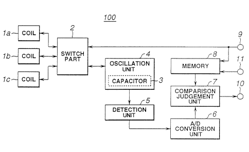
Fig. 1 is a block diagram showing a schematic structure
of a coin detecting device.
Coin detecting device 100 comprises coils 1 (1a to lc),
switching unit 2, oscillation unit 4 including capacitor 3,
detection unit 5, A/D conversion unit 6, comparison judgment
unit 7, memory 8, input terminal 9, output terminal 10, and
input terminal 11.
In the coin detecting device 100, t:he coils 1 are
connected in parallel with the capacitor 3 of the oscillation
unit 4 via the switching unit 2. The switching unit 2
connects any one of the co_Cls la to lc t;o the capacitor 3
according to a changeover ;signal which i.s sent from a control
(not shown) and input through the input terminal 9. Coil 1
(one of la to lc) connected with the capacitor 3 through the
switching unit 2 configure: an oscillation circuit, which has
the oscillation unit 4, the, coil 1 and t;he capacitor 3 as the
circuit structure elements.. The oscillation unit 4
configured as described above, when the coil 1 does not act on
the coin electromagnetical:ly, continues to oscillate at the
resonance frequency of coi:L 1 and capacitor 3 based on a
predetermined oscillation condition and outputs a fixed AC
voltage signal. On the other hand, when coil 1 acts enough on
the coin, the output of thE~ oscillation unit 4 changes for the
reasons described afterward.
Therefore, the output (AC voltage signal) of the
7
CA 02290516 2001-12-20
oscillation unit 4 is converted by the detection unit 5 into
t:he DC voltage signal which corresponds to the output of the
oscillation unit. The DC voltage signa:L is converted into a
digital signal by the A/D conversion unit 6. This digital
:signal is compared with a fixed value stored in the memory 8
ray the comparison judgment unit 7 to judge the presence or not
of the coin, and the judgment result is output from the output
germinal 10.
The memory 8 selects a fixed value to be output to the
comparison judgment unit 7 according to the changeover signal
t:o be input in the switching unit 2 and can set the fixed
value to an arbitrary value via the input terminal 11.
Fig-. 2 is a diagram showing a structure of the coil 1.
The coil 1 comprises T-type ferrite core 21, bobbin 22
fitted to the ferrite core 21 and coil 23 wound around bobbin
2.2 and is connected to the switching unit 2 or the capacitor 3
through lead 24.
Each unit which composes the coil 1 can be mounted on
casing 20 according to a technical demand for an environmental
resistance and the like.
For instance, as shown in Fig. 3, the coil 1 is disposed
i.n the neighborhood of coin storing unit 30 (corresponding to
coin storing unit 530 of Fig. 12 described in BACKGROUND ART)
a.nd detects that coins 31 :more than a predetermined number are
Filed up in coin storing unit 30.
The structure of coin detecting device 100 shown in Fig.
1 will be described in detail with reference to Fig. 4.
Fig. 4 is a diagram showing an example of circuit to
8
CA 02290516 2001-12-20
achieve the coin detecting device 100 shown in Fig. 1.
In the circuit shown .in Fig. 4, coils la to lc have
imductances configured of coils L1, L2, L3 (L1=L2=L3)
respectively. And, switching unit 2 for selectively switching
the coils la to lc comprisE~s P channel MOS-type FETs Trl, Tr2,
T:r3. The capacitor 3 is a capacitor having electrostatic
capacity C2. Oscillation unit 4 comprises operation amplifier
A:L connected so that the coil 1 {any of la to lc) is connected
in parallel to the capacitor 3 via the switching unit 2 so to
form an oscillation circuii~, a CR series circuit of resistor
R:L and the capacitor C1 connected to form a positive feedback
circuit of the operation amplifier A1, and resistors R2, R3
connected to determine gain of the operation amplifier A1.
Detection unit 5 comprises a voltage doubler rectifier circuit
o:E diodes D1, D2 and an ini~egrating circuit of resistor R4 and
capacitor C4. A/D conversion unit 6, comparison judgment unit
7 and memory 8 comprise MPU (microprocessor unit) 40 to which
interface terminal 41 and output terminal 42 are connected.
The switching unit 2 makes switching to selectively
connect one of coils la, lb, lc to capacitor 3 in oscillation
unit 4. This switching operation is effected with the gate
voltage of the MOS-type FE'.Cs (Trl, Tr2, Tr3) controlled by
switch signals S1, S2, S3 output from MPU 40.
Now, operation of the oscillation unit 4 will be
described.
Fig. 5_is a circuit diagram for illustrating oscillation
unit 4.
Oscillation unit 4, wizen coil 1 does not detect a coin,
9
CA 02290516 2001-12-20
oscillates at a fixed frequency and when coil 1 detects a
coin, its output level changes (the oscillation may stop
occasionally).
When it is assumed that impedance of positive feedback
circuit 51 (series circuit of capacitor C1 and resistor R1) of
operation amplifier 52 (A1) is Z1 and impedance of parallel
circuit 50 of coil 1 (inductance L) and capacitor 3
(electrostatic capacity C2) is Z2, Z1 and Z2 are expressed
respectively by the expression (1) and 1=he expression (2:).
Z1= R1- j ~I ... ~1)
r 1
1 jwLx~-~ ~C2~
Z2 = 1 1 - 1 . . . ~2)
~~L+=1 jwL-j~C2
j~C2
When it is assumed that a current flowing the circuit is
i., a ratio of input voltage Vi, output voltage Vo and I/O
voltage is expressed by the expression (3).
Vo = ~Zl + Z2~
Vi=Z2xi
Yo Zl + Z2
Vi Z 2
_ 1 + Z1
Z2
R1- j 1
=1 + wCl
1
jcvLx~_ j ;~
1
j ~L - .1 ~C-2
1+ Cl -~-~zClxl.~+'~ ~2xR1-~L~ ...~3)
c
to
CA 02290516 2001-12-20
Here, input voltage Vi. and output voltage Vo become in
phase because the feedback circuit of operation amplifier 52
i:~ a positive feedback circuit. Therefore, imaginary number
part in the expression (3) is zero, leading to the expression
(~~). Accordingly, oscillation frequency f0 of oscillation
unit 4 is expressed by the expression (5).
rvC2xRl- Rl =0
wL
~2 _ 1
C2 x L
.~.tv= 1
C2xL
_ l
f 0 - 2~ C2 x L "' ~5)
When oscillation frequency f0 is shown by the expression
(:i), the relation between input voltage 'Vi and output voltage
Vo is expressed by the,expx-ession (6). oscillation condition
to continue the oscillation is expressed by the expression (7)
because Vo/Vi indicates vo7.tage amplification Av of the
arnplification circuit.
_ ~6
Vii l.~ Cl +wzClxL '~ t )
Av>_1+C-2+ z l~..L+J ~c~C2xRl-R~
Cl ~ C C
~l
CA 02290516 2001-12-20
Oscillation unit 4 continues oscillating while the
er:pression (7) is held, and. an AC voltage signal of sine wave
is. output at the output of oscillation unit 4, In an actual
circuit, the value of each unit is adjusted to fulfill the
e~:pression (7) in a state that coil 1 does not make a mutual
electromagnetic reaction with the coin.
In oscillation unit 4 well adjusted as described above,
coil 1 reacts electromagnet:ically with the coin, namely,
permeability is changed because the coin exists in the
nE:ighborhood of coil 1, the: value of inductance L changes into
L', and the condition shown by the expression (8) is
established to terminate oscillation.
Av<1+C2+ 1 --+j wC2xR1-~L'y ...~g~
Cl ~ZClxL'
Output (AC voltage signal) of oscillation unit 4 is input
to detection unit 5 and detected and rectified by diodes D1.
and D2, then converted into a DC voltage signal by an
integrating circuit composed of resistor R4 and capacitor C4.
This DC voltage signal is converted into a digital signal in
A!D conversion unit 6 and compared in comparison judgment unit
7 with a given value stored in memory 8.
Comparison with a fixed value in comparison judgment unit
7 is not to detect only the termination of oscillation
described above but to detect a change in output level (even
tine voltage level and the :Frequency are acceptable) of the
oscillation unit 4 from a change in inductance L (including a
change of impedance and g involved) since coil 1 and the coin
12
CA 02290516 2001-12-20
ac;t electromagnetically. And, each part of the oscillation
unit 4 is easily adjusted as compared with the case that the
tE:rmination of the oscillation only is detected.
Comparison judgment unit 7 outputs a signal, which
indicates that the coins of more than the fixed number are in
the coin storing unit 30 (see Fig. 3), from output terminal 42
when a value of 'the digital signal input from A/D conversion
unit 6 is smaller than the fixed value stored in memory 8.
Memory 8 can rewrite a. given value stored in it by an
external device (not shown) connected to interface terminal 41
o~E MPU 40 and also stores a plurality of given values at the
same time, so that it can switch values to be output to
comparison judgment unit 7 based on switch signals S1, S2, S3
which are output by MPU 40 to select one of coils la, lb, lc.
Values output to comparison judgment unit 7 are switched for
each coil because effects on inductance and Q of the coils are
variable depending on the types of coins (material and
thickness) detected by coi7_s la to lc.
Referring to Fig. 6 and Fig. 7, a process of the coin
detection by coin detectin<~ device 100 shown in Fig. 1 will be
described.
Fig. 6 is a flowchart showing a process of the operation
of the coin processor to which the coin detecting device 100
is applied. Fig. 7 is a f:Lowchart showing a process of the
coin detection.
A coin processor (not shown) installed in an automatic
vending machine starts to operate when power supply is turned
on (step 101), and input, output and the like of MPU are
13
CA 02290516 2001-12-20
initialized (step 102). When the initialization is completed,
the coin processor stands by until a coin or coins are
inserted into the vending machine (NO in step 103). When a
coin is inserted (YES in step 103), identification processing
is performed to judge true or not and money type of the
inserted coin (step 104).
When the inserted coin. is judged as counterfeit money by
the coin identification processing in step 104 (NO in step
105), this coin is returned. as the counterfeit money (step
106). If it is judged as true money (YES in step 105), coin
shoring unit inspection processing is performed (step 107).
Coin storing unit inspection processing will be described
bE~low .
Coin storing unit ins>ection processing is to detect
whether the coin storing unit contains coins to be paid out as
change. The presence of coins-is detected by coin detecting
device 100 shown in Fig. 1. When coin detecting device 100
starts coin storing unit inspection processing (step 201), MPU
40 turns on switch signal ~al (step 202). When switch signal
S1 is turned on, switching unit 2 connects coil la with
oscillation unit 4. The output of oscillation unit 4 is
converted into a digital dE;tection signal by detection unit 5
and A/D conversion unit 6 I;step 203). Comparison judgment
unit 7 compares a value of the detection signal with a fixed
value stored in memory 8 (step 204). When the value of the
detection signal is smaller than the fixed value (YES in step
204), a signal indicating 'that the pertinent money type is
stored more than the fixed number is output as a detected
14
CA 02290516 2001-12-20
result (step 205).
MPU 40 turns on switch signal S2 (step 206), and then in
the same manner as above, switching unit 2 connects coil lb to
oscillation unit 4, output ~of oscillation unit 4 is converted
into a digital detection signal by detection unit 5 and A/D
conversion unit 6 (step 207). Comparison judgment unit 7
compares a value of the detection signal with a value of the
fixed value stored in memory 8 (step 208;), and when the value
of the detection signal is smaller than the fixed value (YES
in. step 208), a signal indicating that the pertinent money
type is stored more than the fixed number is output as a
deaected result (step 209).
Then, MPU 40 turns on switch signal S3 (step 210), and
then in the same manner as above, switching unit 2 connects
coil lc to oscillation unit 4, output of oscillation unit 4 is
converted into a digital detection signal by detection unit 5
and A/D conversion unit 6 (step 211). Comparison judgment
unit 7 compares a value of the detection signal with a value
oi° the fixed value stored i.n memory 8 (step 212), and when the
v~ilue of the detection signal is smaller than the fixed value
( S~ES in step 212 ) , a signal. indicating that the pertinent
money type is stored more than the fixed number is output as a
dEatected result (step 213). And the coin storing unit
inspection processing is ts:rminated (step 214).
When the coin storing unit inspection processing is
terminated (step 107), it is judged whether change can be paid
oat or not based on the inspection result, the amount of money
inserted, and the price of commodity (step 108). If change
CA 02290516 2001-12-20
cannot be paid out (NO in step 109), the inserted coin is
returned (step 110). Hut, if change can be paid out,
c~~mmodity is discharged and change is paid out at the same
time (step 111). Then the device stands by for the next
insertion of coins ( step 1()3 ) .
A second embodiment o:E the method and device of detecting
a coin according to the present invention will be described.
Fig. 8 is a diagram showing an example of the circuit of
the coin detecting device :in the second embodiment.
Coin detecting device 100' comprises coils 1' (1'a to
1'c), switching unit 2', capacitors 3' (3'a to 3'c),
oscillation unit 4', detection unit 5', A/D conversion unit
6', comparison judgment unit 7', memory 8', an input terminal
(not shown), and an output terminal (not: shown). Coils 1'a to
1'c have inductances made ~of coils L1, L2, L3 respectively,
and switching unit 2' for selectively switching coils 1'a to
1'c is composed of P channel MOS-type F>JTs Trl, Tr2, Tr3.
Capacitors 3'a, 3'b, 3'c are capacitors having electrostatic
capacity C2, and oscillation unit 4' comprises operation
amplifier A1 which is connected to form an oscillation circuit
having as circuit structure elements coil 1' (one of 1'a to
1.'c) and capacitor 3' (any of 3'a to 3'c and corresponding to
coils 1'a to 1'c) connected in parallel to the coil 1' via
switching unit 2'; CR series circuit of capacitor C1 and
resistor R1 connected so t:o form a positive feedback circuit
of operation amplifier A1; and resistors R2, R3 connected so
i~o determine gain of operation amplifier A1. Detection unit
'.i' comprises a voltage doLUbler rectifier circuit consisting of
16
CA 02290516 2001-12-20
diodes D1, D2, and an integration circuit consisting of
resistor R4 and capacitor t~4. A/D conversion unit 6',
comparison judgment unit 7' and memory ~' are composed by MPU
40' to which interface terminal 41' and output terminal 42'
are connected.
This coin detecting device 100' hay: capacitor 3, which is
contained in oscillation unit 4 of coin detecting device 100
(see Fig. 1 and Fig. 4) in the first embodiment, as capacitor
3' in a number corresponding to the number of coils 1'. The
capacitors 3' are connected in parallel with coils 1' at coin
detecting positions, and a pair of coil 1' and capacitor 3' is
selectively connected to oscillation unit 4' by switching unit
2' to detect a coin. Principle and operation of coin detection
are the same as those of the coin detecting device 100 in the
first embodiment and are omitted from being described.
In the embodiments described above, the coil shown in
F'ig. 2 is used to detect the coin, but another coil may be
used to detect the coin.
Fig. 9 is a diagram showing the structure of a coil
different from the one shown in Fig. 2.
In Fig. 9, coil 301 comprises T-type ferrite core 321,
~~obbin 322 attached to ferrite core 321, coil 323 wound around
bobbin 322 and lead 324 and is housed in casing 320. Hole 325
corresponding to a diameter of T-type ferrite core 321 is
formed on casing 320, and ferrite core 321 is protruded from
hole 325. Coil 301 is disposed in coin storing unit 330 (Fig.
Si corresponds to Fig. 3) to detect that coins 331 are
accumulated.
17
CA 02290516 2001-12-20
Coil 301 has better sensitivity of Q compared with coil 1
shown in Fig. 2 because ferrite core 321 is protruded from
casing 320.
Fig. 10 is a diagram ~;howing an example of comparison
bEaween coil 1 and coil 301 for Q.
In the drawing, a broken line shows a relation between Q
oj° coil 1 and coin-to-coil distance 1 in a certain conditian,
and a solid line shows a relation between Q of coil 301 and
coin-to-coil distance 1 in the same condition (materials of
coil and ferrite core, temperatures and others).
It is seen from Fig. 10 that coil 301 having ferrite core
3:?1 protruded from casing 320 tends to have better Q as
compared with coil 1. Coin, detecting sensitivity can be
innproved by using coil 301.
Where hole 325 is formed on casing 3 20 as coil 301, it: is
h<ird to make potting of the: coil with a .liquid, and an effect
oj= dirt prevention may also be lowered. It is also seen from
Fig. 10 that when housed in airtight casing 20 as coil 1 is,
sE:nsitivity of Q is improved when a distance to the coin
bE:comes short. Therefore, when the coil is housed in the
a:Lrtight casing, sensitivity of Q can be improved by making a
coil-coin distance short.
Fig. 11 is a diagram showing an example of coil having
irnproved Q .
In Fig. 11, coil 401 comprises T-type ferrite core 421,
bobbin 422 mounted on ferrite core 421, coil 423 wound around
bobbin 422, and lead 424. And ferrite core 421 is protruded
from bobbin 422. Coil 40I is housed in airtight casing 420
18
CA 02290516 2001-12-20
which contains protruded ferrite core 421.
Casing 420 has a partly protruded shape because coil 401
has ferrite core 421 protruded. Therefore, hole 430a is
formed on coin storing unit 430 where coil 401 is fitted. And
coil 401 is mounted so to insert the protruded part of casing
9:20 into hole 430a.
By configuring as described above, a distance between
coil 401 and coin 431 is made short as compared with coil 1
shown in Fig. 2, and sensitivity of Q can be improved.
In the embodiments described above,. detection of the
presence of coins in the coin storing unit by the coin
processor was described. And a coil may also be disposed near
the coin passage to detect that a coin has passed through the
passage. In addition to the T-type ferrite core, the coil
type may use a pot-type core, and the core unit in a coil
using various forms of cores can be protruded to improve
sensitivity.
INDUSTRIAL APPLICABILITY
The invention relates to a method and device to detect
coins, which is configured to selective7_y connect one of a
plurality of coils to an oscillation unit by a switch and to
detect the presence of coins based on output from an
oscillation circuit comprising the connected coil and the
oscillation unit. Hy configuring as described above, mutual
interference among the plurality of coils can be eliminated,
and adjustments such as temperature correction can be made
with ease.
19
CA 02290516 2001-12-20
Different types of coins can be detected and detection
accuracy can be improved b;y changing a predetermined value to
be compared with output fr~~m the oscillation circuit when the
coil is switched.
Furthermore, adjustment of the oscillation circuit and
the like is not required but a switch is additionally mounted
when the number of coils i:~ increased to detect coins.
Therefore, the same circuit can be used for a variety of
u;s age .