Note: Descriptions are shown in the official language in which they were submitted.
CA 02290541 1999-11-22
WD 98/54554 PCT/GB98/01379
A Thermal Detector Array
The invention relates to a composite thermal detector array comprising an
array of discrete
thermal detector elements. The array may be a linear or a two-dimensional
array. Linear arrays
are particularly suitable for applications where there is relative motion
between the detector head
and any objects being imaged. Two-dimensional detector arrays are used in a
wide range of
infrared imaging applications.
Thermal detectors such as ferroelectric detectors and resistance bolometers
are of interest due to
their operation at ambient temperatures unlike the photon (or semiconductor)
detectors which
require cryogenic modules for cooling. Development of thermal detectors is
currently directed
towards the achievement of arrays having large numbers of elements with small
inter-element
pitch, and to enhancing the level of temperature discrimination that may be
observed in the scene
above the inherent noise level in the detector array and the imaging system
designed for the
viewing of the video image.
Linear and two-dimensional arrays of thermal detectors have been constructed
using, as the
?o radiation sensitive element. both ferroelectric materials and also
resistance bolometer materials.
the latter from a range of oxide. metal and semiconductor materials.
Ferroelectric wafers
prepared from ceramic blocks and polished to thin sections have been bonded to
the silicon
readout integrated circuitry (IC) directly by metal bump bonding as described
in US Patent
4.142.207. This patent further emphasises the desirability of improving the
thermal isolation of
35 the detector element from the silicon IC by bonding to the top of thin
metal columns fabricated
on the silicon IC, one for each element. Improved thermal isolation (i.e. low
thermal conductance
to the element) is necessary to secure high responsivity from the element when
absorbing
infrared radiation focused from the scene. The bump bonding process may
involve a cold-weld
between metal surfaces or a solder bump bond between wettabie metal pads on
the element and
3o the input circuitry of the silicon IC [D J Pedder, Hvbrid Circuits, L'ol. I
~. p-1. 1988].
CA 02290541 1999-11-22
. . .. ..,. .. ..
.. .. .. .. . . . . . .
. ... . . .
, .. ...
. . . . . .
2 , , ... ... .. ... .. ..
In US Patent 5,450,053 the thermal isolation of the detector elements is
obtained by the
construction of arrays of microbridge structures on the surface of the silicon
readout integrated
circuitry (ROIC) such that there is one microbridge per element. The
microbridge supports the
detector element above the IC on thin and narrow legs to achieve the low
thermal conductance.
The detector element material is deposited as a thin film on or as the
microbridge structure and is
provided with suitable electrodes to collect the signal and pass this down the
legs to the silicon
readout circuitry in the IC. The technique of depositing resistance bolometer
material enables
the fabrication of a large array of resistance micro-bolometers. The technique
enables the
1 o fabrication of higher performance detector arrays than those fabricated
using the bump bonding
technique due to the lower thermal conductances that may be achieved.
It has been proposed [R. Watton, Ferroelectrics, Vol. 133, pp. 5-10, 1992]
that ferroelectric
thermal detector arrays of high performance may be fabricated using
microbridge structures. The
ferroelectric material may be deposited by various techniques, sol-gel
processing, rf magnetron
sputtering, laser ablation or MOCVD. However, a severe limitation in the
deposition of the
ferroelectric film onto the microbridge structures is the limit on the
temperature that the silicon
IC, which acts as substrate with the array of microbridge structures, can be
raised to during the
deposition. The silicon IC maximum temperature is restricted to the region of
500°C to avoid
2o damage to the circuitry providing the array readout functions (i.e.
amplification and element
matrix switching). However is has been proposed that to achieve good
ferroelectric properties in
the deposited ferroelectric film high substrate temperatures may be required
either in the
deposition process or in subsequent annealing [R Watton, ibid. and R Watton,
Integrated
Ferroelectrics, Vol. 4, pp175-186, 1994].
US 3 801 949 relates to a thermal detector device in which an array of
detector elements is
fabricated on a silicon substrate containing the readout circuitry for the
detector elements. A thin
layer of silicon dioxide, deposited on the substrate, thermally insulates the
substrate from the
detector elements during detection of infrared radiation. The detector
elements are fabricated on
the substrate containing the detector readout circuitry prior to the etching
of openings in the
substrate which also serve to thermally isolate the detector elements from the
circuitry during
detector operation. However, as described previously, the problem exists that
the silicon subtrate
AMEr~aED SHEET
CA 02290541 1999-11-22
.. .... .. ..
.. .. .. .. . . . . . .
. . . . . . ... . . .
. . . . . ... ...
. . . . . . .
3 . . ... ... .. ... .. ..
containing the readout circuitry cannot withstand the elevated temperatures
required to fabricate
detector elements having good ferroelectric properties.
It is known that there exists an incompatibility between the temperatures
required in the
deposition or annealing of the ferroelectric films, to obtain the most
favourable properties for
thermal detector arrays, and the temperature limits set by avoidance of damage
to the
metallisation and circuits on the silicon readout IC. For example, annealing
sputtered films of
the ferroelectric lead scandium tantalate to temperatures between 800°C
and 900°C results in
to ferroelectric properties in the films which approach those measured in the
ceramic material used
in the bump bonded technology described previously [R Watton and MA Todd,
Ferroelectrics,
Yol. 118, pp279-295, 1991 ]. Such values of ferroelectric properties, if
combined with the higher
thermal isolation of the microbridge element structures, would result in very
high performance
thermal detector arrays.
It has also been proposed that ferroelectric films of both lead zirconate
titanate and lead
scandium tantalate can be deposited or annealed at temperatures in the region
of 500°C but with
reduced values of those ferroelectric properties which determine the imaging
performance of
thermal detector arrays [R Watton, Ferroelectrics, Yol. 184, pp 141-I50,
1996]. The reduced
2o values do not preclude a useful imaging performance from arrays prepared by
these processes but
significant improvements in performance will be available if the temperature
limitation were
removed.
The temperature limitation problem outlined above is overcome by the present
invention. The
invention relates to a composite structure for thermal detector arrays which
allows the fabrication
of ferroelectric element arrays on microbridge structures at higher
temperatures than those
presently allowed by the limitation of avoidance of damage to the readout
integrated circuitry.
AluttiVDED ~tFT
CA 02290541 2005-07-19
29756-156
4
According to one aspect of the invention, there is
provided a thermal detector device comprising: an array of
thermal detector elements for detecting infrared radiation
and generating output detector signals, an array of
microbridge structures carrying said detector elements,
wherein each microbridge structure includes a common contact
and an output contact, wherein each of the common contacts
is in electrical contact with the each of the other common
contacts, readout integrated circuitry having a plurality of
input contacts, for processing the output detector signals,
and an interconnect layer, having front and rear surfaces,
thermally isolating the array of microbridge structures from
the readout integrated circuitry and comprising a plurality
of interconnect channels between said front and rear
surfaces, wherein the interconnect channels provide an
electrical correction between the output contact of each of
the microbridge structures at the front surface of the
interconnect layer and the associated input contact on the
readout integrated circuitry at the rear surface of the
interconnect layer such that the microbridge structures are
in electrical contact with, but are separated from, the
readout integrated circuitry, wherein the interconnect layer
is a wafer which supports the array of microbridge
structures during fabrication of the latter and in that the
input contacts of the readout integrated circuitry are
substantially vertically aligned with the output contacts.
At the rear face of the interconnect layer, the
interconnect channels may be bump bonded to the input
contacts of the readout integrated circuitry.
In addition to the detector elements, each
microbridge structure may also comprise additional support
layers. Additional support layers may be required, in
CA 02290541 2005-07-19
29756-156
4a
particular, for microbridge structures comprising thin
detector elements which do not provide sufficient support
themselves.
In a preferred embodiment, the detector elements
may be comprised of a ferroelectric material.
. CA 02290541 1999-11-22
. . .. .... .. ..
, .. ~. .. .. . . . . . .
. . , , ~ . . ~ ... . . .
, . ~ . . . . ~ . ... ...
. . ~ . ~ . .
, , ... ... .. ... .. ..
The interconnect channels may each comprise a channel of electrically
conducting material, for
example polysilicon or an electroplated, chemically plated or vapour deposited
metal. Each
5 interconnect channel may further comprise a channel of dielectric material
for electrically
isolating the conducting material from the interconnect layer material.
Typically, the dielectric
material may be an oxide or a nitride layer formed from the interconnect layer
material.
The interconnect layer may be any one of silicon, glass or a ceramic material
or any other
1o material capable of supporting conducting channels in the interconnect
layer. Alternatively, the
interconnect layer may be electrically conducting or semi-conducting material.
Preferably, the
interconnect layer material is thermally matched 'in thermal expansion
properties to the
underlying silicon layer.
Typically, each of the detector elements may have an electrical capacitance of
between 1
picofarad and 1 nanofarad and, preferably, the electrical capacitance of each
interconnect
channel is at least less than one tenth of the electrical capacitance of each
ferroelectric detector
element.
25
AMEt~DEp SHE~1'
CA 02290541 2005-07-19
29756-156
6
According to a second aspect of the invention,
there is provided a method of fabricating a thermal detector
device, the method comprising the steps of; (i) providing an
interconnect layer having front and rear surfaces, wherein
the interconnect layer is a wafer comprising a plurality of
interconnect channels between said front and rear surfaces,
(ii) fabricating an array of thermal detector elements as an
array of microbridge structures on the front surface of the
interconnect layer, wherein each microbridge structure
includes a common contact and an output contact, each of the
common contacts being in electrical contact with each of the
other common contacts and each interconnect channel being in
contact with the output contact on one of the microbridge
structures, and (iii) subsequently bonding the interconnect
channels at the rear surface of the interconnect layer to
readout silicon integrated circuitry, such that the
microbridge structures are in electrical contact with, but
are separated from, the readout integrated circuitry.
The method may further comprise the step of
fabricating at least one additional support as part of the
microbridge structures. The interconnect channels may be
formed by a reactive ion etch technique.
The thermal detector elements may be fabricated as
part of the microbridge structures by means of a deposition
process. The fabrication of the array of thermal detector
elements may also include the step of annealing the thermal
detector elements. Preferably, at least one of the
deposition process or the annealing process is carried out
at a temperature well above the limiting temperature which
applies to processing directly on the silicon readout wafer.
For example, at least one of the deposition process or the
CA 02290541 2005-07-19
29756-156
6a
annealing process may be carried out at a temperature of at
least 500°C and, more preferably, at a temperature of at
least 700°C.
CA 02290541 1999-11-22
WO 98/54554 PCT/GB98/01379
7
The invention will now be described, by example only, with reference to the
following figures in
which;
Figure 1 shows a schematic sectional view of a part of thermal detector array
of the invention,
comprising a silicon interconnect layer,
Figure 2 shows a schematic sectional view of a part of a thermal detector
array, comprising a
porous ceramic interconnect layer,
to
Figure 3 shows an enlarged plan view of one of the microbridge structures in
Figure 1,
Figure 4 shows a schematic plan view of the array of microbridge structure
elements in the
thermal detector array and
Figure 5 shows a schematic plan view of an alternative configuration of the
array of microbridge
structure elements in the thermal detector array.
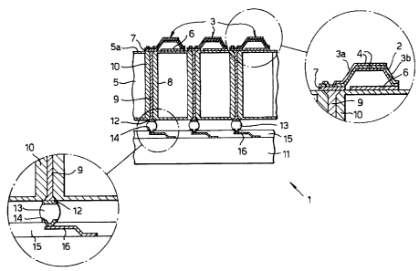
Figure 1 shows a schematic cross sectional diagram of part of a thermal
detector device 1,
2o comprising an array of detector elements 2 fabricated as an array of
microbridge structures 3.
Three microbridge structures 3 are shown, although the complete device may
comprise any
number of microbridge structures in a linear or a two dimensional array (e.'~.
256 x 128 or 256 x
256).
Each microbridge structure 3 has two 'legs' 3a,3b. In the example shown, each
microbridge
structure 3 comprises two electrode layers 4 which sandwich the detector
element 2 and provide
the electrodes for the microbridge structure 3, one associated with each leg
3a,3b. Typically, the
detector elements 2 may be comprised of a ferroelectric material which rnav be
fabricated as the
microbridge structure 3 by deposition or annealing or a combination of both
processes.
3o
CA 02290541 1999-11-22
WO 98/54554 PCT/GB98/01379
The detector elements 2 may provide sufficient support to form the microbridge
structure
themselves (the electrodes 3 do not provide any support). However, other
support layers (not
shown) may also be required to reinforce the microbridge structures. In
particular, additional
support layers may be required for microbridge structures comprising thin
detector elements 2
which cannot provide sufficient support.
The array of microbridge structure 3 is fabricated on the front surface of a
wafer of substrate
material 5. For the purpose of this specification, this wafer of substrate
material 5 shall be
t0 referred to as the 'interconnect layer' or the 'interconnect wafer'. The
two electrode layers 4 on
each microbridge structure 3 make contact with metal layers or electrodes 6
and 7 on the surface
of the interconnect layer ~. The metal layer 6 forms a common electrode,
connecting one leg 3b
of each microbridge structure 3 in a common connection (i.e. the metal layer 6
is joined between
microbridge elements 3). The metal layers 7, one metal layer 7 being
associated with each
15 microbridge structure 3, are connected to the other leg 3a of each
individual microbridge
structure 3. If the interconnect layer 5 is a silicon wafer, the wafer 5 may
be coated on both front
and rear surfaces with a passivating dielectric layer Sa, as shown in Figure
1. The electrode
layers 4 collect the output signals from the detector elements 2 and pass them
down the legs
3a,3b to the metal layers 6,7. An important feature of the interconnect layer
~ is that it contains
2o no active circuitry, only the common metal layer 6 which runs across the
top surface of the layer
The interconnect layer 5 also comprises an array of electrically conducting
channels 8, one
channel per microbridge structure 3. The channels 8 shall be referred to as
the "interconnect
25 channels". The interconnect layer ~ may be silicon, glass or a ceramic
material, or any other
material which is able to support the interconnect channels 8. Preferably, the
material is
thermally matched in thermal expansion properties to the underlying silicon.
CA 02290541 1999-11-22
WO 98/54554 PCT/GB98/01379
9
The interconnect channels 8 are shown to run substantially vertically through
the interconnect
layer S from its front surface to its back surface. The conducting
interconnect channels 8 may be
formed by filling holes or pores. penetrating through the interconnect layer
~. with an electrically
conducting filament 9. These electrically conducting filaments 9 may be set
into a dielectric
material 10 such that they are electrically isolated from the bulk material of
the interconnect
layer 5, for example if a silicon interconnect layer is employed.
The thermal detector device 1 also comprises readout integrated circuitry
(ROIC), typically
formed on a readout silicon wafer 11, for processing the output signals from
the detector
elements 2. On the front surface of the interconnect layer ~, each
interconnect channel 8 is in
contact with the metal layer 7 in contact with leg 3a of the relevant
microbridge structure 3 via
electrode layer 4. Each interconnect channel 8 is therefore in electrical
contact with the
associated detector element 2. Output signals from the detector elements 2 are
therefore passed
down the legs 3a,3b to the metal layers 6,7, and from the metals layers 7, the
signals are passed
through the interconnect channels 8. The interconnect layer ~ therefore
provide a means of
conducting the output signals from the detector elements 2 to the readout
wafer 11 whilst the
interconnect layer ~ physically separates the microbridge structures 3, and
hence the detector
elements 2, from the readout wafer 11.
At the rear surface of the interconnect Layer 5 the interconnect channels 8
are connected to
electrically conducting pads I2. Solder bonds 13 may be used to connect these
electrically
conducting pads 12 to input pads 14 on the silicon readout wafer 11. The
process of bump
bonding using solder would be conventional to one skilled in the art.
The input pads 14 on the silicon readout wafer 11 may be arranged on
dielectric passivation or
intermetallic dielectric layers 15. For clarity, Figure 1 shows layer 15 as a
single layer, although
in practice this layer may comprise at least two dielectric layers. Within
this layer (or layers) 15 ,
the input pads 14 are connected to metal layers 16 which form part of the
metallisation structure
on the readout wafer 11. The metal layers 16 connect the signal at the input
pads 14 to
subsequent pre-amplifier inputs (not shown).
CA 02290541 1999-11-22
W-O 98/54554 PCT/GB98/01379
For the thermal detector device shown in Figure 1, the fabrication of the
microbridge structures
3, and the subsequent deposition or annealing of the ferroelectric detector
material 2, may be
performed prior to the bump bonding of the silicon readout wafer 11 to the
interconnect layer 5.
Temperature restrictions on the deposition or annealing of the ferroelectric
material 2 are
therefore not restricted by the silicon readout wafer 11 and the survival of
its circuitry, but only
by the interconnect layer ~ and the materials used for the common electrode
and the electrically
conducting contacts and channels.
1 o Preferably, in order to achieve higher ferroelectric thermal detector
performance, the fabrication
of the ferroelectric material as the microbridge structures needs to be
carried out at a temperature
greater than it is possible to achieve in the fabrication of device
configurations where the silicon
readout wafer is directly connected to the microbridge element and the
ferroelectric material. For
such known device configurations, this temperature limitation is typically
between 450°C and
is 550°C. As the detector performance increases with the deposition or
annealing temperature of the
ferroelectric material, carrying out the ferroelectric deposition or anneal at
higher temperatures
then this gives enhanced detector performance. Even higher temperatures (e.g.
700 °C - 900°C)
result in further enhanced performance devices. The present invention is
advantageous in that it
enables such higher fabrication temperatures to be used and therefore enables
higher
2o performance ferroelectric thermal detector arrays to be fabricated.
The process of fabricating the ferroelectric material 2 as the microbridge
structures 3 may be
achieved by the deposition of the ferroelectric material, preferably at a
temperature greater than
500°C, or more preferably at even higher temperatures e.g. greater than
700"C. Alternatively, the
3s fabrication process may involve initially depositing the material on the
microbridge structure and
then subsequently annealing the material, in which case the deposition process
may be carried
out at a lower, more practicable temperature and the anneal carried out at a
higher temperature to
achieve the required detector performance. The processes of depositing or
annealing the detector
elements would be conventional to one skilled in the art.
3o
CA 02290541 1999-11-22
WL198/54554 PCT/GB98/01379
11
The interconnect layer 5, its common electrode 6, its through-wafer
interconnect materials,
including any electrically conducting and insulating materials which are used,
are chosen so as
to allow high deposition or annealing temperatures for the ferroelectric
material. The materials
must therefore be able to withstand temperatures in excess of 500°C,
and preferably temperatures
greater than 700°C. For the purpose of this specification, a material
capable of withstanding the
required deposition or annealing temperature shall be taken to mean a material
that does not
melt, crack, split or delaminate at the deposition or annealing temperature.
1 o The interconnect layer 5 may be a silicon wafer or a glass or a ceramic
material, for example
Pyrex glass T"" or alumina, which are similar to silicon in terms of thermal
expansion, or any
other material capable of supporting the interconnect channels 8 and
preferably thermally
matched in thermal expansion properties to the underlying silicon. Typically,
the conducting
material 9 in the interconnect channels 8 may be polysilicon, which may be
conveniently
deposited from its gaseous phase. Alternatively, the conducting filament may
be formed using
vapour deposited, electroplated or chemically plated metals, e.g. copper,
gold, tungsten or nickel
or may be formed from a diffused channel of aluminium. Typically, the
dielectric material 10 in
the interconnect channels 8 may be an oxide or nitride layer formed from the
interconnect layer
material or may be a deposited film of dielectric material.
After fabrication of the microbridge structure array at an elevated
temperature required for
enhanced ferroelectric properties, the interconnect layer 5 may be solder bump
bonded to the
silicon readout layer 11 via the solder bonds 13 which wet the metal pads 12
and 14. This may be
done using solder and known techniques. Alternatively, the bond between metal
pads 12 and 14
may be performed by coating the surfaces to be connected with a suitable metal
to give a cold
weld on contact and pressure.
CA 02290541 1999-11-22
W-O 98/54554 PCT/GB98/01379
12
In order to avoid stress and damage arising through the temperature used for
solder bonding,
preferably a requirement of the material of the interconnect wafer 5 is that
it should be matched
closely in thermal expansion to the silicon readout wafer 11. Materials such
as silicon itself and
some glasses, including Pyrex glasses T"", are particularly suitable with
thermal expansions
varying by less than 30% from that of silicon. As mentioned previously, if a
silicon
interconnect layer 5 is used then it is preferable to electrically isolate the
electrically conducting
channels 9 from the bulk material of the interconnect layer 5.
l0 Typically, the interconnect layer 5 may have a thickness of between 0.1-I
mm and, preferably, is
in the region of 0.5 mm thick such that it provides sufficient rigidity for
the processing steps to
be performed on its upper and lower surfaces. Typically, the diameter of the
interconnect
channels 8 may be between 10-50 p.m (Figures 1 and 2 are not drawn to scale).
15 Alternatively, in order to ease the formation of the interconnect channels
8 through the
interconnect layer 5, the layer 5 may be thinned to the region of 100-200 p.m
thickness over the
area of the elements of the array within a surrounding "picture frame" of
thicker support material
(i.e. over the area of the microbridge structures 3 of the array). Such a
layer 5 would also be
mechanically stable to allow the fabrication of the array of microbridge
structures 3.
Porous silicon technology [e.g. V. Lehmann, J. Electrochem. Soc., Vol. 143,
No. l, pp. 385-390,
January 1996] may be used to etch the interconnect channels 8 in a silicon
interconnect wafer 5.
This technology enables small diameter pores or channels to be etched through
silicon wafers
with large aspect (length/diameter) ratios. Using this technique, it is
possible to achieve a
substantially regular array of interconnect channels 8 in the silicon
interconnect layer 5. The
walls of the interconnect channels 8 may be oxidised prior to the deposition
of, for example, the
polysilicon conducting material 9. The oxidation of the walls of the
interconnect channels 8 and
the deposition of polysilicon conducting material 9 are conventional
techniques used in
microelectronic manufacturing. Alternatively, the interconnect channels 8 may
be etched in a
3o regular array through a silicon wafer by a reactive ion etch technique
using reactive gases in a
plasma.
CA 02290541 1999-11-22
WO 98/54554 PCT/GB98/01379
13
Figure 2 shows an alternative embodiment of the invention, comprising an
alumina interconnect
layer 5. As before, the microbridge structures 3 are shown with two legs
3a,3b, and comprise the
ferroelectric material 2 sandwiched between two electrode layers 4. In this
configuration, the
interconnect layer 5 is shown as having an array of microchannels (or
micropores) 17 capped
with an electrically insulating material Sa, except in regions where through-
wafer connections
are required (shaded microchannels 18). In these regions, the microchannels 18
are filled with a
metal by electroplating, chemical plating or other method so that they form
the required
conducting means. Alternatively, it may be more convenient to fill all of the
microchannels with
to a metal and those microchannels which are not required to provide a
connection are capped with
an electrically insulating material Sa. For interconnect layers made of
ceramic or glass material,
it would not be necessary to insulate the conducting filaments from the bulk
interconnect layer
material itself.
15 If an alumina interconnect wafer is used, electrochemical anodisation
techniques may be used to
form the microchannels 17,18 in the interconnect layer 5 (e.g. 'Theoretical
modelling ofporous
oxide growth on aluminium', MSaito et al, J. Phys. D: Appl. Phys. 25, pp 1258-
1263, 1992). If
the process of electrochemical anodisation is used, the microchannels 17,18
formed in the
interconnect layer 5 will typically be irregularly spaced, as illustrated in
Figure 2. In this case,
2o where the spacing of the microchannels 17,18 is not regular, or if the
number of microchannels
does not match the number of microbridge structures 3, and hence the number of
detector
elements 2, groups of microchannels may be used collectively to form the
required
interconnections in positions corresponding to the positions of the
microbridge structure
electrodes 7. What is important is that the interconnecting groups of
microchannels are
25 substantially regularly spaced, such that they provide a connection to the
regularly spaced
microbridge structures 3. This may be achieved by filling or capping the
microchannels 18 with
oxide (or electrically insulating material) 5a except where through-layer
interconnections are
required. Standard electroplating techniques can be used to provide the
metallic filling in these
contact areas. For example, using an alumina interconnect wafer S in this way,
uniform
3o microchannels, typically having a diameter up to 60 nm, may be formed to a
depth in the region
of typically 100 pm.
CA 02290541 1999-11-22
Wa 98/54554 PCT/GB98/01379
14
If a glass interconnect layer is used, and is thinned to the region of 100-200
~m thickness over
the area of the elements of the array, the glass would be mechanically stable
to allow the
fabrication of the array of microbridge structures. However, the temperature
allowed for
deposition or annealing in the fabrication of the detector elements would be
limited to the
softening temperature of the glass, e.g. in the region of 600°C. A
ceramic membrane such as
alumina would permit much higher temperatures to be used.
It is important that the geometry and construction of common electrode 6 and
the interconnect
1 o channels do not impose a high stray electrical capacitance at the input to
the silicon readout
wafer as this will reduce the device performance. The responsivity derived
from the ferroelectric
detector material when it absorbs infrared radiation imaged from the scene is
inversely
proportional to the sum of the detector element capacitance and the stray
capacitance at the input
to the subsequent amplifier (not shown). The stray capacitance must therefore
be kept small
15 compared with the detector element capacitance.
The invention is concerned with thermal detector arrays having an inter-
element pitch (i.e. the
spacing of the detector elements 2) in the range 100 ~,m down to 25 ~.m. The
thickness of the
deposited ferroelectric material 2 will vary from 1 ~m down to 0.1 Vim.
Relative permittivity of
2o the ferroelectric materials used for the detector elements will vary from
300 up to 5000
dependent on the actual material and its operating electrical bias and
temperature. The element
capacitance therefore could range from 1 picofarad to 3 nanofarad, but will
preferably be 2 to 50
picofarad.
25 For example, using a silicon interconnect wafer, as shown in Figure 1, the
interconnect channels
8 may be formed by etching channels of the order of 20 ~.m thick through the
interconnect layer
5, coating the channel with oxide having a thickness of several microns and
filling with a central
core 9 of an electroplated metal. Such.an interconnect channel 8 has a
capacitance in the region
of 0.3 picofarad per millimetre thickness of silicon. Thus an interconnect
layer 5 having a
3o thickness of a fraction of a millimetre will ensure that the stray
capacitance is maintained at a
level well below the detector element capacitance, as desired.
CA 02290541 1999-11-22
Wa 98/54554 PCT/GB98/01379
IS
To avoid cross-coupling between elements due to stray capacitance between
adjacent
interconnect cores 9, it may be preferable to use a conducting or semi-
conducting interconnect
wafer 5 having a suitable electrical conductivity such that it may be
connected to the common
electrode 6, farming a common earth for the array elements. For example, an
interconnect wafer
of silicon may be doped by conventional techniques used in microelectronic
engineering to
achieve the required conductivity.
Figure 3 shows a enlarged plan view of a simplified, single microbridge
structure 3 of the array
to shown in Figure 1. The two legs 3a,3b are shown sloping down on either side
of the top electrode
layer 4, underneath which is the detector element 2 and the lower metal layer
5 (layers 2 and S
are obscured in Figure 3), with the base of the leg 3a in contact with the
metal layer 7 on the
front surface of the interconnect layer 5. The position of contact is shown to
be approximately at
the centre of the base of the leg 3a in this representation, although this
contact may be made at
I5 any point along the base of the leg 3a. To make a suitable contact between
the base of the leg 3a,
through the electrode layer 4, and the metal layer 7 requires suitable
metallisation on the surface
of the interconnect layer 5 to give a contact area of at least 1 ~m2. In this
figure, the conducting
channel 9 of the interconnect channel goes into the page. The geometry of the
structure shown in
Figure 3 is not expected to give the lowest thermal conductance from the
element to the
20 interconnect wafer and structures having narrower, longer legs extending
down the sides of the
element, or folded underneath, may be preferred and would be known to one
skilled in the art.
Figures 4 and 5 show plan views of the composite thermal detector device i and
show two
different configurations of the microbridge structure orientation. For
clarity, not all of the
25 microbridge structures 3 and their components have been numbered and the
detailed structure of
each microbridge and the interconnect layer are not shown. In Figure 3, the
microbridge
structures 3 all have a like orientation such that the legs 3a,3b, and
therefore the metal contacts
6,7 (see Figure 1), are regularly spaced. This orientation is compatible with
an interconnect layer
having regularly spaced interconnect channels 8, as shown in Figures 1 and 2.
CA 02290541 1999-11-22
WO 98/54554 PCT/GB98/01379
16
As the diameter of the channels formed through the interconnect layer 5 may
vary by up to a
large fraction of the interconnect channel pitch, more than one filamentary
conductor may be
established in an individual interconnect channel 8 without there being an
electrical connection
between separate conductor filaments. In the configuration shown in Figure 5,
the microbridge
structures 3 are therefore oriented such that, for example, the contacts on
the legs 3a of four
adjacent microbridge structures 3 are in close proximity, thereby leading to a
simplification of
the electrode geometry on the surface of the interconnect layer 5. Geometry's
such as this,
however, do involve more closely packed geometry's for the solder or bump
bonds in the
1 o interfacing of the ROIC.
The orientations of the microbridge structures 3 on the surface of the
interconnect layer are not
restricted to the particular geometry's shown in the examples in Figures 4 and
5.
I5 The thermal detector device I is advantageous in that higher fabrication
temperatures may be
used to deposit or anneal the detector elements on the microbridge structures,
therefore enabling
high performance ferroelectric or microbolometer thermal detector arrays to be
fabricated. The
method of fabricating the device is therefore easily compatible with silicon
processing
techniques.
25