Note: Descriptions are shown in the official language in which they were submitted.
CA 02290620 1999-11-12
WO 98/52042 PCT/US98/09838
1
MOLECULAR WIRE IN 1ECTION SENSORS
Background of the Invention
The present invention relates to biosensors and chemical sensors. More
particularly,
it relates to sensors having a chemical or biochemical species detection group
connected to an
electronic circuit by electrically conducting polymer strands.
Biosensors employing enzymes have been applied to the detection of numerous
analyte species concentrations including glucose, cholesterol, or both glucose
and
cholesterol concentrations in whole blood samples. Such sensors and associated
instruments employ an enzyme capable of catalyzing a reaction at a rate
representative of the
selected compound concentration in an assay mixture.
There are three general detection approaches employing a glucose enzyme
electrode.
The first and earliest measures oxygen consumption. The oxygen-sensing probe
is an
electrolytic cell with a gold (or platinum) cathode separated from a tubular
silver anode by an
I S epoxy casting. The anode is electrically connected to the cathode by
electrolytic gel, and the
entire chemical system is isolated from the environment by a thin gas-
permeable membrane
(often Teflon). A potential of approximately 0.8V (from solid-state power
supply) is applied
between the electrodes. The oxygen in the sample diffuses through the membrane
and is
reduced at the cathode with the formation of the oxidation product, silver
oxide, at the silver
anode. The resultant current is proportional to the amount of oxygen reduced.
The analyzer
unit operates over the range from 0.2 to 50 ppm of dissolved oxygen. Gases
that reduce at
0.8V will interfere; these include the halogens and SO~. H,S contaminates the
electrodes.
A second approach detects H202 production but requires an applied potential of
approximately 0.65V {from solid-state power supply) applied between the
electrodes, one of
which is inside a pertnselective membrane. The H~O, in the sample diffuses
through the
permselective membrane (if one is present) and is oxidized at the anode. Many
metal, metal
complexes, nonmetal, organic and biochemical species that oxidize at
approximately 0.65V
will interfere; such as ascorbic acid, amines, hydrazines, thiol compounds,
catechols,
hydroquinones, ferrocenes, and metalloporphyrins. The inside permselective
membrane is
not always capable of removing the complicated mix of possible interferences
from the
analyte matrix.
A third approach takes advantage of the fact that the enzymatic reaction
requires two
steps. First, the enzyme glucose oxidase (GOD) (EC 1.1.3.4) is reduced by
glucose, then
CA 02290620 1999-11-12
WO 98/52042 PCT/US98/09838
2
the reduced enzyme is oxidized to its initial form by an electron acceptor,
i.e., a mediator. In
natural systems, the mediator is oxygen. In biosensors, another mediator
compound may be
employed to transfer electrons between the enzyme and a conductive surface of
an electrode
at a rate representative of the enzyme catalyzed reaction rate when an
appropriate potential is
applied to the particular redox mediator in use. Such biosensors may employ
amperometric
measurements to determine glucose concentration in a whole blood sample. This
involves
an integrated sample measurement of the area under the ampere versus time
curve,
corresponding to the amount of glucose in the sample.
The mechanism by which a common amperometric sensor works is depicted in
Figure 1. A sensor 2 employs glucose oxidase (GOD), for example, as a
molecular
recognition group. Glucose oxidase catalyzes the oxidation of glucose to
gluconolactone in
analyte 4. This reaction involves the FAD/FADH2 redox center of the enzyme.
Sensor 2
includes a molecular recognition group, region 6, attached to an electrode 8.
When glucose
in analyte 4 contacts GOD-FAD (glucose oxidase including the FAD redox center)
in region
6, it is oxidized to gluconolactone. At the same time, the GOD-FAD is reduced
to GOD-
FADH2. This involves two electrons and two hydrogen ions being transferred to
the FAD.
Normally, in the absence of a sensor mediator, the GOD-FADH2 is reoxidized by
atmospheric oxygen to GOD-FAD to complete the catalytic reaction. In the
presence of a
mediator, however, the GOD-FADH2 is sometimes reoxidized by a mediator (Mox).
In this
case, the GOD-FADH2 releases two hydrogen ions to analyte 4 and two electrons
to the
mediator. The resulting reduced mediator (Mred) may then be reoxidized by
electrode 8 at
an appropriate potential. The reoxidation of the mediator is accompanied by
the transfer of
an electron or electrons to electrode 8. This is the current that is monitored
to provide a
concentration of glucose.
In theory, a mediator may be any small molecule inorganic, organometallic or
organic compounds, which are reduced by the enzyme, and oxidized by an
appropriate
applied potential at the electrode surface. The mediator should be designed to
rapidly and
efficiently transfer electrons between the enzyme and the electrode.
Otherwise, ambient
oxygen would oxidize nearly all of the reduced GOD and the desired signal
would be very
weak. The mediator should also transfer a total charge proportional to the
glucose or
cholesterol concentration in the sample. The current which results from the
mediator
oxidation is known as the Cottrell current which, when integrated with respect
to time, gives
the number of coulombs associated with the sensor reaction. The total coulombs
passed is
proportional to the amount of analyte.
Unfortunately, mediators are commonly provided as mobile "reagents" which
diffuse
to the enzyme where they are oxidized or reduced (depending upon the reaction
catalyzed by
the enzyme). The oxidized or reduced mediator then diffuses to the electrode
surface where
CA 02290620 1999-11-12
WO 98/52042 PCTNS98/09838
3
it gains or loses an electron. Unfortunately, such mechanism is dependent upon
the
continuing presence of recycled mobile mediators. As such compounds can leak
from the
electrode surfaces, there may be a gradual depletion in available mediator and
a consequent
reduction in sensor sensitivity. Examples of diffusing redox mediators include
dyes (e.g.,
methylene blue), ferrocene derivatives (Cass, AEG; Davis, G; Francis, GD;
Hill, HAO;
Aston, WJ; Higgins, IJ; Plotkin, EV; Scott, LDL; Turner, APF: Ferrocene-
Mediated
Enzyme Electrode for Amperometric Determination of Glucose. Anal. Chem. 56:667-
671,
1984), components of conducting organic metals and quinones.
Also, available sensors applying the above amperometric approach to the
detection of
glucose, cholesterol, lactate, H202, NAD(P)H, alcohol, and a variety of other
compounds in
whole blood samples, can have other serious complicating problems. For
example, the
percentage of sensor surface area covered by blood can vary; sometimes the
blood sample
does not cover the entire electrode. This may be caused by a poorly adherent
enzyme (often
applied by spraying) thus allowing leakage of blood or other analytes along
the edges of the
electrode. A related problem results from hydration of the reaction area prior
to test. This
dilutes the ligand (e.g., glucose) concentration and therefore gives a lower
reading than
would be accurately given by an unhydrated surface.
Further, the partial pressure of molecular oxygen (OZ) may complicate the
interpretation of sensor data. Molecular oxygen is the natural electron
acceptor mediator of
the enzyme glucose oxidase (GOD). Following oxidation of D-(+)-glucose by GOD,
reduced glucose oxidase (GODre~,) will transfer electrons to OZ forming HZOZ
in the absence
of other mediators. In amperometric glucose biosensors described above, the
unwanted OZ
side reaction competes with synthetic chemical mediators for electrons
supplied by the
GOD~ea enzyme. Calibration of GOD-based biosensors at different altitudes
(i.e., different
partial pressures of OZ) may be a problem if electron transfer rates of
selected synthetic
chemical mediators are not orders of magnitude faster than the Oz side
reaction.
Humidity (i.e., HZO) may be another potential problem if mass action of HBO
and O
present drives the enzyme catalyzed oxidation product of D-gluconoiactone in
reverse back
to the reduced starting material, D-(+)-glucose. Catalase, a common
contaminant of glucose
oxidase preparations, may be driven in reverse by mass action of excess H20
and O
producing 2 moles of H202. H~OZ buildup combined with D-gluconolactone could
drive the
glucose oxidise reaction in reverse by mass action back to D-(+)-glucose.
Other problems associated with known amperometric sensors include, for
example,
( 1 ) difficulty in fitting the Cottrell current curve (i.e., ampere-time
graph), (2) sampling with
enough frequency to accurately obtain the time integral of Cottrell current,
(3) high applied
potential at the electrode causing indiscriminate oxidation or reduction of
interfering
CA 02290620 1999-11-12
WO 98/52042 PCT/US98/09838
4
substances, and (4) complicated electronic circuits requiring potentiostat and
galvinostat
mstrumentarion.
Some of the above drawbacks of the current amperometric biosensors have been
noted and analyzed {see, Schuhmann, W: Chap. 9. Conducting Polymers And Their
Application In Amperometric Biosensors. In: Diagnostic Biosensor Polymers. ACS
Symposium Series 556. Usmani, AM; Akmal, N; eds. American Chemical Society;
Washington, D.C.; 1994; pp. 110-123). First, due to the fact that the active
site of redox
enzymes is in general deeply buried within the protein shell, direct electron
transfer between
enzymes and electrode surfaces is rarely encountered. This is especially true
for enzymes
which are integrated within non-conducting polymer membranes in front of the
electrode
surface. Hence, electron transfer is usually performed according to a
'shuttle' mechanism
involving free-diffusing electron-transferring redox species for example the
natural electron
acceptor Oz or artificial redox mediators like ferrocene derivatives (Cars,
AEG; Davis, G;
Francis, GD; Hill, HAO; Aston, WJ; Higgins, IJ; Plotkin, EV; Scott, LDL;
Turner, APF:
Ferrocene-Mediated Enzyme Electrode for Amperometric Determination of Glucose.
Anal.
Chem. 56:667-671, 1984), osmium complexes (Heller, A: Electrical Wiring of
Redox
Enzymes. Acc. Chem. Res. 23(5):128-134, 1990), or quinones. Due to the
necessity for
the redox mediators to diffuse freely between the active sites of the enzymes
and tile
electrode surface, these electrodes show a limited long-term stability as a
consequence of the
unavoidable leaking of the mediator from the sensor surface. Additionally in
the case of the
natural redox couple O~/H2O2, the sensor signal is dependent on the 02 partial
pressure, and
a high operation potential has to be applied to the working electrode giving
rise to possible
interferences from cooxidizable compounds. The second drawback is related to
the
fabrication of these sensors. The physical assembling of an enzyme membrane
and an
electrode is extremely difficult to automate and thus in principal
incompatible with
microelectronic fabrication techniques. Additionally, the miniaturization as
well as the
integration of individual biosensors into a miniaturized sensor array is
impossible with
techniques which are mainly based on the manual deposition of a droplet of the
membrane-
forming mixture onto the electrode surface.
Consequently, the next generation of amperometric enzyme electrodes has to be
based on immobilization techniques which are compatible with microelectronic
mass
production processes and easy to miniaturize. Additionally, the integration of
all necessary
sensor components on the surface of the electrode has to prevent the leaking
of enzymes and
mediators simultaneously improving the electron-transfer pathway from the
active site of the
enzyme to the electrode surface.
In addition to amperometric mechanisms, which rely on detecting current
generated
from faradaic reactions, a potentiometric mechanism may be employed to sense
analyze
CA 02290620 1999-11-12
WO 98/52042 PCTNS98/09838
concentration. Potentiometric techniques monitor potential changes between a
working
electrode and a reference electrode in response to charged ion species
generated from enzyme
reactions on the working electrode. A very common potentiometric sensor is the
pH sensor
which registers changes in hydrogen ion concentration in an analyte. A
microelectronic
5 potentiometric biosensor, the Field Effect Transistor (FET) biosensor, has
generated some
interest. In this design, a receptor or molecular recognition species is
coated on a transistor
gate. When a ligand binds with the receptor, the gate electrode potential
shifts, thereby
controlling the current flowing through the FET. This current is detected by a
circuit which
converts it to an observed ligand concentration. Observed problems with
potentiometric
systems include, for example, { 1 ) slow response of the electrode (i.e.,
seconds), (2)
complicated electronic circuits for three electrode (i.e., working, counter,
and reference
electrode) electrochemical systems requiring potentiostat instrumentation, (3)
low sensitivity,
and (4) limited dynamic range.
Recently, two groups {Heller et al. and Skotheim et al.) have explored and
developed
redox polymers that can shuttle electrons from the enzyme to the electrode.
The groups have
"wired" the enzyme to the electrode with a Long redox polymer having a dense
array of
electron relays. Each relay is a redox site bound to the polymer backbone.
Electrons move
along the polymer by hopping from one redox appendage to the next. The polymer
penetrates and binds the enzymes, and is also bound to the electrode.
Hcller et al. have conducted work on Os-containing redox polymers. They have
synthesized a large number of such Os-containing polymers and evaluated their
electrochemical characteristics (Gregg, BA; Heller, A: Redox Polymer Films
Containing
Enzymes. 1. A Redox-Conducting Epoxy Cement: Synthesis, Characterization, and
Electrocatalytic Oxidation of Hydroquinone. J. Phys. Chem. 95:5970-5975, 1991
). Their
most stable and reproducible redox polymer is a poly(4-vinyl pyridine) to
which
Os(bpy)ZC12 has been attached to 1/6th of the pendant pyridine groups. The
resultant redox
polymer is water insoluble. To make it water soluble and biologically
compatible, Heller et
al. have partially quaternized the remaining pyridine pendants with 2-
bromoethyl amine.
The redox polymer is water soluble and the newly introduced amine groups can
react with a
water soluble epoxy e.g., polyethylene glycol diglycidyl ether and GOD to
produce a cross-
linked biosensor coating-film. Such coating-films produced high current
densities and a
linear response to glucose up to 600 mg/dL (United Stales Patent 5,262,035 to
Gregg et al.).
Heller describes the electrical wiring of redox enzymes for- use as
amperometric
biosensors (Heller, A: Electrical Wiring of Redox Enzymes. Acc. Chem. Res.
23(5):128-
134, 1990). The Holler approach is an improvement over amperometric enzyme
electrodes
based on diffusing redox mediators, including dyes, ferrocene derivatives,
components of
conducting organic metals, and quinones, all described above. In the Holler
approach,
CA 02290620 1999-11-12
WO 98/52042 PCT/US98/09838
6
redox centers of a redox polymer polycation (e.g., 2[Os-(2,2'-
bipyridine)z(poly(vinylpyridine))Cl]'+~z+) are electrostatically and
covalently bound to the
enzyme and relays electrons to the electrode, on which a segment of the
polycation is
adsorbed. Binding of the redox polymer polycation to the electrode can be
electrostatic
when the electrode has a negative surface charge.
Fluctuations in current with partial pressure of oxygen (e.g., oxygen
concentration in
blood), depend on the ratio of the rate of direct electroxidation of the FADHz
centers to their
rate of oxidation by molecular oxygen, and therefore on the rate of electron
transfer to, and
the electrical resistance of, the three-dimensional wired-enzyme structure. At
high osmium-
complex concentrations, and in sufficiently thin layers, the competition is
won by electron
transfer to the electrode via the osmium centers, and the electrodes are
relatively insensitive
to oxygen (Heller, A: Electrical Wiring of Redox Enzymes. Acc. Chem. Res.
23(5):128-
134, 1990. Gregg, BA; Heller, A: Cross-Linked Redox Gels Containing Glucose
Oxidase
for Amperometric Biosensor Applications. Anal. Chem. 62:258-263, 1990.
Surridge, NA;
Diebold, ER; Chang, J; Neudeck, GW: Chap 5. Electron-Transport Rates In An
Enzyme
Electrode For Glucose. In: Diagnostic Biosensor Polymers. ACS Symposium Series
556.
Usmani, AM; Akmal, N; eds. American Chemical Society; Washington, D.C.; 1994;
pp.
47-70).
Electrodes based on conducting polypyrroles with ferrocenes also have been
reported
(Hale, PD; Inagaki, T; Karan, HI; Okamoto, Y; Skotheim, TA: A New Class of
Amperometric Biosensor Incorporating a Polymeric Electron-Transfer Mediator.
J. Am.
Chem. Soc. 111 (9):3482-3484, 1989).
Skotheim et al. have used flexible polymer chains to act as relays. Their
polymers
provide communication between GOD's redox centers and electrode. No mediation
was
found when ferrocene was attached to a non-silicone backbone. Their ferrocene-
modified
siloxane polymers were said to be stable and non-diffusing (Boguslavsky, LI;
Hale, PD;
Skotheim, TA; Karan, HI; Lee, HS; Okamoto, Y: Novel Biosensors For Specific
Neurotransmitters Based On Flavoenzymcs And Flexible Redox Polymers. Polym.
Mater.
Sci. Eng. 64:322-323, I 991 ).
Unfortunately, the redox polymer systems of Heller et al. and Skotheim et al.
have a
limited electron transfer rate based on electron hopping between dense
electron relay pendant
groups. Further, their "wire" redox centers must be designed to undergo
reaction at a
potential close to that of the enzyme catalyzed reaction. The closer the
potential is to the
redox potential of the enzyme itself, the lesser the likelihood that a
potentially interfering
substrate will be spuriously oxidized. Unfortunately, to address this issue
limits the range of
polymer redox couple and molecular headgroup combinations.
CA 02290620 1999-11-12
WO 98/52042 PCTNS98109838
7
A fundamental presupposition for the construction of reagentless amperometric
enzyme electrodes is the design of a suitable electron-transfer pathway from
the active site of
the enzyme to the electrode surface. According to Marcus theory (Marcus, RA;
Sutin, N:
Electron Transfers In Chemistry And Biology. Biochim. Biophys. Acta 811:265-
322,
1985) a redox mediator with a low reorganization energy after the electron
transfer has to be
able to penetrate into the active site of the enzyme to shorten the distance
between the
prosthetic group (e.g., FAD/FADHZ) and the mediator. Hence, the rate constant
of the
electron-transfer reaction can be increased. After this 'first' electron
transfer the redox
equivalents have to be transported to the electrode surface via mechanism
having a rate
constant which is in the range of the turnover rate of the enzyme. In the
shuttle mechanism
mentioned above (having mobile mediators), the electron transport involves
diffusion of
redox mediators. In the "wired" redox polymer sensors described above,
electron transport
involves hopping from one redox center to the next on the polymer backbone.
In a recent study, Aizawa et al. discuss a reversible electron transfer
between the
prosthetic group of pyrrolo quinoline quinone (PQQ) enzyme (fructose
dehydrogenase) and
an electrode through a molecular interface (Aizawa, M; Khan, GF; Kobatake, E;
Haruyama,
T; Ikariyama, Y: Chap. 26. Molecular Interfacing of Enzymes on the Electrode
Surface. In:
Interfacial Design and Chemical Sensing. ACS Symposium Series 561. Mallouk,
TE;
Harrison, DJ; eds. American Chemical Society, Washington, D.C., 1994, pp. 305-
313).
The PQQ moieties of randomly oriented fructose dehydrogenase (FDH) which are
very close
to the transducer electrode can easily transfer their electrons to the
electrode (Shinohara, H;
Khan, GF; Ikariyama, Y; Aizawa, M: Electrochemical Oxidation and Reduction of
PQQ
Using a Conducting Polypyrrole-Coated Electrode. J. Electroanal. Chem. 304:75-
84, 1991.
Khan, GF; Shinohara, H; Ikariyama, y; Aizawa, M: Electrochemical Behaviour of
Monolayer Quinoprotein Adsorbed on the Electrode Surface. J. Electroanal Chem.
315:263-
273, 1991 ). However, the prosthetic groups of FDH located far from the
electrode can not
provide their electrons, as the distance from the electrode exceeds the
maximum electron
transfer distance (~25 A). Therefore, to make the FDH (EC 1.1.99. I 1, MW :
141,000) on
the electrode surface electrochemically active, Aizawa et al. introduced an
ultrathin
conductive polypyrrole (PP) membrane as a molecular interface as "wiring" to
assist the
electron transfer from PQQ to the electrode. Unfortunately, the wiring used by
Aizawa is
randomly oriented and does not necessarily present enzyme at optimal position
with respect
to the analyte.
What is needed is an improved sensor design that rapidly transfers electrons
from
headgroup redox reactions to an electrode, does not rely on a redox relay such
as freely
diffusing mediators, and optimally orients the headgroup with respect to the
analyte.
CA 02290620 1999-11-12
WO 98/52042 PCT/US98/09838
8
A great number of approaches for microfabrication of chemical sensors are
currently
under way, particularly in the areas of field effect transistor (FET)-based
chemical sensors,
metal oxide gas sensors, and biosensors. Since Janata et al. first reported
micro-enzyme
electrodes based on FET (Cams, S; Janata, J: Field Effect Transistor Sensitive
to Penicillin.
Anal. Chem. 52:1935-1937, 1980), a number of groups have been employing
microfabrication techniques (e.g., photolithography) such as those employed in
semiconductor device technology to fabricate micro-enzyme electrodes. Despite
enormous
efforts of many groups, the FET-based micro-enzyme electrodes of practical use
have not
been realized yet, largely because of the problems associated with
potentiometric methods
general lack of a fast response, high sensitivity, and wide dynamic range.
For the construction of reagentless enzyme electrodes (e.g., electrodes
analogous to
those of Heller et al. and Aizawa et al.) one has to focus on a technique for
the modification
and functionalization of electrode and even micro-electrode surfaces to allow
the strong
binding of the enzyme and the redox mediator taking into account the
presuppositions for an
effective and fast electron transfer between the enzyme and the electrode.
These features
requirements are in principle met with enzyme electrodes based on redox-
sensitive
hydrogels, however, the manual deposition of these hydrogels is not compatible
with mass-
production techniques.
The electrochemical deposition of conducting-polymer layers occurs exclusively
on
the electrode surface and can hence be used for the immobilization of enzymes
either
covalently using functionalities on the polymer film or physically entrapped
within the
growing polymer film. As the conducting-polymer film itself does not
participate in the
electron transfer, mediator-modified enzymes entrapped within a polypyrrole
layer have been
used for the construction of a reagentless oxidase electrode.
Electrochemical deposition methods of the prior art typically use high current
density
and voltage potential conditions which destroy the orderly Helmholtz double-
layer at the
electrode surface (United States Patent 5,215,631 to Westfall). Resulting
disorderly
depositions at electrode surfaces produce random polymer structures which lack
orientational
and positional order. Aizawa et al. "wired" PQQ-FDH in their sensors with
ultrathin
conductive polypyrrole (PP) membrane as a molecular interface. Electrochemical
synthesis
of molecular-interfaced FDH on Pt electrode was prepared by the following two
steps: ( 1 )
potential-controlled adsorption of FDH, and (2) electrochemical polymerization
of
polypyrrole. These steps employ high voltage and current density
electrochemical
deposition conditions to produce polymer (FDH and polypyrrole) depositions on
the Pt
electrode that are randomly oriented. Therefore, this device must operate at
high 0400 mV}
operating potential resulting in possible interfering cooxidizable species.
CA 02290620 1999-11-12
WO 98/52042 PCT/US98/09838
9
What is needed is an improved technique for depositing molecular recognition
groups and associated wiring, if necessary, that provides a strong direct
connection between
an electrode and the molecular recognition groups, and allows the molecular
recognition
groups to be aligned in a common orientation.
CA 02290620 1999-11-12
WO 98/52042 PCT/US98/09838
Summary of the Invention
In one aspect, the present invention provides a sensor for sensing the
presence of an
analyte component without relying on redox mediators. This sensor may be
characterized as
including the following elements: (a) a plurality of conductive polymer
strands each having
5 at least a first end and a second end and each aligned in a substantially
common orientation;
(b) a plurality of molecular recognition headgroups having an affinity for the
analyte
component and being attached to the first ends of the conductive polymer
strands; and (c) an
electrode substrate attached to the conductive polymer strands at the second
ends.
The polymer strands in a common orientation resemble liquid crystals.
Preferably,
10 the strands are oriented substantially orthogonal to the electrode
substrate. The conductive
polymer strands may be, for example, one or more of multi-stranded nucleic
acids, electron
transport proteins, synthetic organic and inorganic conducting polymers, metal
crystallite
molecular wires, and Langmuir-Blodgett conducting films. In a particularly
preferred
embodiment, the conductive polymer strands are double-stranded DNA strands.
The headgroup may participate in a redox reaction when contacting a molecule
of the
analyte component. When this is the case, a mobile charge carrier is
transferred directly to a
conductive polymer strand attached to the headgroup, without participating in
a redox
reaction in the polymer strand. In one embodiment, the molecular recognition
headgroups
participate in the redox reaction by catalyzing a chemical transformation of
the analyte
component. Examples of such headgroups include oxidoreductases and catalytic
antibodies.
In one specific example used repeatedly in this specification, the headgroup
is glucose
oxidase.
The sensor headgroups may be chemically homogeneous (e.g., they are all
glucose
oxidase) or chemically inhomogeneous (e.g., they include a mixture of glucose
oxidase,
cholesterol oxidase, and cholesterol esterase). In one preferred embodiment,
when the
headgroups are inhomogeneous, the sensor includes a first region on the
electrode substrate
where a first group of chemically homogeneous molecular recognition headgroups
is located
and second region on the electrode substrate where a second group of
chemically
homogeneous molecular recognition headgroups is located. The first and second
regions
may be separately addressable so that information signal from the two regions
may be
separately processed and able to indicate whether cholesterol, glucose, or
both cholesterol
and glucose are present in the analyte for example.
The electrode substrate should be capable of reporting to an electronic
circuit
reception of mobile charge carriers from the conductive polymer strands. In
one specific
embodiment, the electrode substrate is a diode such as a photovoltaic diode.
More generally,
CA 02290620 1999-11-12
WO 98/52042 PCT/~JS98I09838
11
the substrate may be a device element of a device on semiconductor chip (e.g.,
a gate on an
FET).
In a variation of this aspect of the invention, a sensor is provided to detect
the
presence of a nucleic acid sequence (at a crime scene for example). The sensor
includes (a) a
plurality of sequence-specific single-stranded nonconductive nucleic acid
wires each having
at least a first end and a second end; and (b) an electrode substrate attached
to sequence-
specific single-stranded nonconductive nucleic acid strands at the second ends
and capable of
reporting to an electronic circuit, reception of mobile charge carriers
originating from
complementary mufti-stranded nucleic acid strands. In this embodiment, when
the sensor is
exposed to an analyte having the complementary nucleic acid sequence, at least
some of the
affixed single-stranded nonconductive nucleic acid wires hybridize or anneal
with the analyte
to form conductive mufti-stranded nucleic acid strands. Thus, charge carriers
can be
transported to the electrode substrate for detection. In one embodiment, the
plurality of
sequence-specific single-stranded nonconductive nucleic acid strands are
attached to
molecular recognition headgroups such that mobile charge carriers are
transferred directly
through only annealed mufti-stranded nucleic acid strands when a redox
reaction occurs at
the attached molecular recognition headgroups.
Another aspect of the invention provides method of detecting a concentration
of an
analyte component in an analyte with a sensor having a structure as described
above. The
method may be characterized as including the following steps: (a) contacting
the molecular
recognition headgroups with the analyte; and (b) determining whether electrons
have been
transferred to the electrode substrate resulting from electrons generated by
the redox reaction
and transferred by the conductive polymer strands to the electrode substrate.
When the
redox reaction occurs at a headgroup, a mobile charge carrier is transferred
directly to a
conductive polymer strand attached to the headgroup, without redox reaction in
the polymer
strand. The method may further involve (c) monitoring a change in an
electronic circuit
connected to the electrode substrate, the change resulting from reception of
mobile charge
carriers from the conductive polymer strands; and (d) correlating the change
in the electronic
circuit with the concentration of the analyte component.
Another important aspect of the claimed invention is a sensor employing a
diode,
preferably a photodiode. Sensors in accordance with this aspect of the
invention may be
characterized as including the following features: (a) a plurality of
molecular recognition
headgroups having an affinity for the analyte component and participating in a
redox reaction
when contacting a molecule of the analyte component such that when the redox
reaction
occurs at a headgroup, a mobile charge carrier is generated; (b) a diode
having a first
electrode to which the plurality of molecular recognition headgroups are
affixed such that
mobile charge carriers generated by the redox reaction are transferred to the
first electrode;
CA 02290620 1999-11-12
WO 98/52042 PCT/US98/09838
12
and (c} a circuit for detecting when the mobile charge carriers are
transferred to the first
electrode. In a preferred embodiment, the plurality of molecular recognition
headgroups are
attached to a p-type side of the diode. Also the diode may be a device on
semiconductor chip
including a plurality of devices.
In a further preferred embodiment, the headgroups are attached through
conductive
polymer strands arranged as described in the above embodiments. Thus, for
example, the
conductive polymer strands may be substantially commonly oriented (e.g.,
orthogonal to the
diode surface).
A diode sensor as described above may be used according to a method as
follows:
(a) contacting the molecular recognition headgroups with the analyte; (b)
specifying a
baseline electrical signal that is present when (i) a stimulus is provided to
the diode and (ii)
the plurality of molecular recognition headgroups are substantially free of
the analyte
component; and (c) detecting a deviation from the baseline electrical signal,
which deviation
results from transfer of the mobile charge carriers to the first electrode
when the analyte
component comes in contact with the molecular recognition headgroups. The
method may
further include (d) determining an amplitude of the deviation; and (e)
determining an analyte
component concentration directly from the amplitude of the deviation without
the use of any
other information from the electrical signal. It has been found that the
analyte component
concentration is sometimes proportional to the amplitude of this deviation.
Depending upon
the type of signal detector employed, the baseline electrical signal and the
deviation from the
baseline electrical signal may be measures of voltage or electrical current.
Preferably,
though not necessarily, the diode is a photovoltaic diode and the stimulus
provided in the
specifying a baseline electrical signal is radiant energy.
Yet another aspect of the present invention is method of forming a sensor
capable of
sensing the presence of an analyte component. This method may be characterized
as
including the following: (a) contacting a sensor substrate (e.g., a device
element of a device
on semiconductor chip) with a first medium containing mobile conductive
polymer strands
or precursors of the conductive polymer strands; (b) applying a first
potential to the substrate
sufficient to form a first structure having the conductive polymer strands
affixed to the
substrate; (c) contacting the sensor substrate, with affixed conductive
polymer strands, with
a second medium containing mobile molecular recognition headgroups; and (d}
applying a
second potential to the substrate sufficient to affix the molecular
recognition headgroups to
the affixed conductive polymer strands. This process produces a sensor
structure in which
the substrate affixed to the conductive polymer strands and the molecular
recognition
headgroups also affixed to the conductive polymer strands.
CA 02290620 1999-11-12
WO 98/52042 PCT/US98/09838
13
Preferably, the step of applying a first potential is performed at a potential
which
causes the affixed conductive polymer strands to be oriented in a
substantially common
direction. This potential may be between about 0.001 and 500 mV, for example.
The step
of applying a second potential is preferably performed at a potential which
causes the affixed
molecular recognition headgroups to be oriented in a substantially common
direction. This
second potential may be between about 0.001 and 500 mV. Preferably, though not
necessarily, the first medium is removed from the sensor substrate following
the step of
applying a first potential. In an alternative embodiment, the second medium is
obtained from
the first medium by performing the step of applying a first potential.
If a sensor having separated regions of different headgroups is to be created,
the
method may also require isolating a region of the sensor substrate prior to
the step of
contacting the sensor substrate with a second medium, such that the molecular
recognition
headgroups are deposited only in the isolated region. To produce multiple
headgroup
regions, the steps of isolating a region, contacting the sensor substrate with
a second
medium, and applying a second potential to the substrate are performed a
second time. The
step of contacting the sensor substrate with a second medium for a second time
employs a
second molecular recognition headgroup, to form a structure having a first
region on the
sensor substrate having a first group of chemically homogeneous molecular
recognition
headgroups and a second region on the sensor substrate having a second group
of
chemically homogeneous molecular recognition headgroups.
Sensors of this invention provide analyte concentration readings, fast
responses,
high sensitivity, high dynamic range, and few erroneous readings. In a glucose
sensor of
this invention, glucose concentration is accurately read despite changes in
partial pressure of
O2, atmosphere, altitude, humidity, or sample application of blood.
Specifically, the direct
wired enzyme sensors of the present invention overcome the difficulty caused
by molecular
oxygen reoxidizing a reduced enzyme before that enzyme (or more precisely its
redox center)
can release electrons to the electrode. This is because the directly wired
sensors of this
invention may provide electron transfer rates many orders of magnitude faster
than
enzymatic reaction rates, and electron transfer rates of diffusional redox
mediators such as
Oz and other artificial mediators. This provides sub-millisecond digital
output from the
sensing chip.
Chips based on device molecular transistors may be reusable, disposable,
reagentless, membraneless. Further, they are amenable to miniaturization and
mass
production, do not require complicated three electrode systems (i.e., no
working, counter,
or reference electrodes) and associated electrochemical instnimentation (i.e.,
no galvinostat
or potentiostat), and provide real-time digital output directly from the chip.
CA 02290620 1999-11-12
WO 98/52042 PCT/US98/09838
14
These and other features and advantages of the present invention will be
described in
more detail below with reference to the drawings.
Brief Description of the Drawings
Figure 1 is a representation of the mechanisms employed in a conventional
redox
mediator based biosensor.
Figure 2 is a representation of a sensor-solution interface in accordance with
this
invention and showing a substrate, molecular wire, and molecular recognition
headgroup.
Figure 3 is a schematic illustration of photodiode sensor in accordance with
an
embodiment of the present invention.
Figure 4A is representation of an electrodeposition step for attaching
molecular wires
to a substrate in accordance with an embodiment of this invention.
Figure 4B is representation of an electrodeposition step for attaching
molecular
recognition headgroups to molecular wires (deposited as shown in Figure 4A) in
accordance
with an embodiment of this invention.
Figure 5 is a graph showing a current signal generated when glucose is
contacted
with a photodiode type GOD glucose sensor in accordance with one embodiment of
this
invention.
Figure 6 is a graph showing current and voltage signals generated when the
sensor
employed in Figure 5 is subjected to a regimen including contact with glucose,
washing,
open circuit, and recontact with glucose.
Figure 7 is a graph showing current and voltage signals generated from a
sensor
employing GDH on a photodiode when exposed to glucose.
CA 02290620 1999-11-12
WO 98/52042 PCT/US98/09838
Detailed Description of the Preferred Embodiments
I . Overview
II. Solid Substrate
III. Sequential Electrochemical and Chemical Deposition Techniques
5 A. Electrochemical Atomic Layer Epitaxy (ECALE)
B . Sequential Monolayer Electrodeposition (SMED)
C. Thin Film Chemical Deposition (CD)
D. Electrochemical Molecular Layer Epitaxy (EMOLE)
1. Deposition of UniaxiaIly Oriented Liquid Crystal
10 Conducting Biopolymers (Proteins and DNA)
IV. Conducting Polymers and Thin Films
A. Electron Transport Proteins
B . DNA Quantum Wires
V. Molecular Recognition Surfaces
15 A. Oxidoreductases (Redox Enzymes)
B . Immunoglobulins
VI. Conduction Mechanisms through Polymers on Solid Substrates
A. Energy Bands in Uniaxially Oriented Liquid Crystal Conducting
Biopolymers (Proteins and DNA) and Semiconductor
Substrates
B . Superconductivity
VII. Applications
VIII. Screening and Assays
IX. Examples
CA 02290620 1999-11-12
WO 98/52042 PCT/US98/09838
16
I. Overview
The present invention relates to sensors, sensor fabrication processes and
semiconductor devices that include the sensors. The sensors and related
devices may be
used for recognizing the presence of, quantitating the amount of, and/or
continuously
monitoring the level of, one or more selected components in a solid, semi-
solid, liquid, or
gas mixture. Preferably, an active molecular recognition surface is "hard
wired" to the
substrate surface (e.g., a semiconductor surface) by an oriented liquid
crystal wire that is
itself conductive. The molecular recognition surface may be of biologically
active material of
the type conventionally employed in sensors. The substrate may be patterned or
unpatterned
and may include (particularly when semiconductors are involved) a conductive
coating such
as a metal between the underlying bulk substrate and the liquid crystal wire.
Hard wiring as that term is used herein may be achieved, in one embodiment,
via
electrochemical fabrication methods described in detail below. Generally, such
methods
make use of low-cost, rapid-prototyping sequential electrochemical and
chemical deposition
techniques such as electrochemical molecular layer epitaxy (EMOLE) which
perform
"molecular wiring" and "molecular soldering" procedures. The liquid crystal
wiring
arrangement preferably provides a "lawn" of commonly oriented "molecular
devices" each
including a single molecular recognition site "headgroup" and attached
molecular wire "tail."
For context, each such device might range in size from about --2 to 2500 A'
surface area
(e.g., enzyme, enzyme co-factor, substrate, supramolecular assembly, cavitand,
host-guest
complex, ligand, receptor, antibody, antigen, etc.).
Biosensors of the present invention may require very low operating potentials.
In a
preferred embodiment, extended conformation of straight uniaxially oriented
liquid crystal
DNA wires are stuck into the GOD active site / redox center of the prosthetic
group
FAD/FADH2, to provide an electron transfer pathway to the surface of a p-n
homojunction
semiconductor solar cell substrate. A pair of electrons per enzyme turnover
event injected
from the wires combine with a pair of holes in the p-type semiconductor layer,
interfering
with the normal photocurrent (i.e., electron / hole pair recombination)
occurring in the solar
cell. The oriented liquid crystal enzyme (molecular recognition headgroup) and
attached
oriented liquid crystal DNA wire tail constitute a molecular transistor. The
device
communicates with a solid substrate (i.e., p-n homojunction) through the
uniaxially oriented
liquid crystal DNA wire tail interconnects. One end of the DNA wire is stuck
in the oriented
liquid crystal enzyme active site / redox center and the other end is stuck
into the p-type
semiconductor layer providing a direct connection between the protein enzyme,
DNA, and
semiconductor substrate.
CA 02290620 1999-11-12
WO 98/52042 PCT/US98/09838
17
In general, the sensors of this invention may be categorized based upon their
transduction and/or gating mechanisms of the headgroup(s): switched or gated
by optical
(optoelectronic), chenucal (chemoelectronic), magnetic (magnetoelectronic),
radioactive
(radioelectronic), thermal (thermoelectronic), mechanical (piezoelectronic),
or electrical
(voltage, current, resistivity, capacitance).
Figures 2 and 3 depict sensors structures in accordance with certain preferred
embodiments of the present invention. Figure 2 presents a cross-sectional view
of a surface
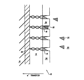
region of a sensor 12. As shown, sensor 12 includes an electrode 14 which is
preferably
made from silicon or another semiconductor substrate. Attached to electrode 14
is a plurality
of conducting polymer strands 16. In a preferred embodiment, each strand is a
DNA
double-stranded molecule. Conductive polymer strands 16 are orientated
substantially in a
common direction which is shown to be normal (orthogonal) to substrate 14.
Strands 16 are
coupled to substrate 14 in a manner that allows direct electrical influence
between these two
features in the sensor. For example, the connection might allow electrons to
be directly
transferred from strands 16 to substrate 14 so that circuitry coupled to
substrate 14 can detect
injection of electrons. In addition, a potential applied to substrate 14 may
influence the
physical state of conductive polymer strands 16.
As will be described in more detail below, a preferred process for affixing
polymer
strands 16 to substrate 14 provides this direct electronic coupling and in
addition orients the
strands 16 along a substantially common axis. Because strands 16 are oriented
in a
substantially common direction, they will sometimes be collectively
characterized herein as a
liquid crystal.
Note that liquid crystal conductive polymer strands such as those shown in
Figure 2
take the form of a "lawn" having first ends attached to molecular recognition
headgroups 18
and second ends attached to electrode 14. As will be described below,
headgroups 18 may
take many different forms. Generally, they should change physical or chemical
state in
response to the presence of a particular component in analyze 20. In a
preferred
embodiment, molecular recognition headgroups 18 are enzymes which undergo a
redox
transformation in response to contact with a specified analyte component. For
example, the
analyte may include a ligand or substrate component 25 which selectively binds
with and is
chemically modified by headgroups 18. Preferably, the chemical modification is
accompanied by generation of electrons which can directly transferred to
strands 16 and
from there to electrode 14. Depending upon the type of molecular recognition
headgroup 18
employed in the sensor 12, the thickness of a hcadgroup layer on top of the
conductive
polymer lawn 16 may be between about 5 and 150 angstroms.
CA 02290620 1999-11-12
WO 98/52042 PCT/US98/09838
18
Importantly, no mediator is required in this sensor design, so electron
transfer is
direct and fast from headgroup 18 to electrode 14. Further, because the
polymer strands 16
are commonly oriented, headgroups 18 are optimally presented for sensing the
desired
anaiyte component. That is, headgroups 18 are not sterically hindered by
polymer strands
16 or other structures.
While the plurality of conductive polymer strands 16 may have a rather uniform
length as depicted in Figure 2, this need not be the case. More frequently,
the individual
polymer strands will have a wide range of lengths. This will be due to
inherent variations in
polymerization techniques or the polymer shearing techniques. Of course, the
distribution of
polymer strand lengths can be made more uniform by passing a raw collection of
polymer
strands through a chromatography column, electrophoretic gel, ultrafiltration
membrane, or
other sizing apparatus. In a preferred embodiment, the average strand length
of conductive
polymer strand 16 is between about 2 and 1,000 A. More preferably, the length
is between
about 10 and 100 A, and most preferably between about 3 and 40 A. When DNA is
employed as the conductive strands, the width of the individual sensor strands
is in the
neighborhood of 20 A.
In a preferred embodiment, the substrate 14 is a p-type electrode of a silicon
photodiode. It may include, though this is not always necessary, a metallic
back plate 22 for
providing an ohmic contact between polymer strands 16 and bulk silicon
electrode 14. Such
back metal plates are conventionally used in semiconductor devices as
terminals for
connection to an external circuit. The back metal plate 22 may be made from
any suitable
conductive metal or alloy, including but not limited to aluminum, copper,
silver, gold, and
platinum. Region 24 represents the close packed liquid crystal spacing between
EMOLE
deposited molecular recognition headgroups. Molecular recognition headgroups
whose
dimensions are greater than the width of underlying molecular wires to which
they are
attached occupy region 24.
In a preferred embodiment, the semiconductor substrate forms part of a
rectifying
diode such as a photodiode. Figure 3 provides a schematic illustration of a
photodiode
based biosensor in accordance with one embodiment of the present invention. A
sensor 50
includes a photodiode 52 including an n-type region 53 and a p-type region 54.
Generally,
any conventional photodiode may be employed with this invention, but it should
have a
surface suitable for affixing conductive polymer strands and molecular
recognition
headgroups as described above. To this end, p-type region 54 may be provided
with or
without a back metal ohmic contact 56 as shown. A plurality of strands of
conductive
polymer 58 are affixed at one end to back-metal plate 56. The other ends of
polymer strands
58 are attached to a collection of molecular headgroups 62. The resulting
structure, as
CA 02290620 1999-11-12
WO 98/52042 PCTNS98/09838
19
illustrated, may be identical with the structure of elements 14, 22, 16 and 18
as shown in
Figure 2.
Photodiode 52 includes a depletion region 60 which automatically forms at the
p-n
semiconductor junction. As is known to those of skill in the art, depletion
regions form at
these interfaces because mobile holes diffuse from p-type regions into n-type
regions just
across the interface where they are combined with electrons available in the n-
type region.
Similarly, mobile electrons in the n-type region diffuse across the interface
to the p-type
region where they combine with holes. As a result, within the reach of charge
carrier
diffusion, essentially all mobile charge carriers are depleted.
When light (or other radiant energy of appropriate wavelength) is shown on a
photodiode such as photodiode 52, some holes and electrons cross the
semiconductor band
gap and provide additional mobile charge carriers which can be drawn out of
photodiode 52
by an applied potential or external short circuit connection. Applied
potentials or external
short circuit connections may be made through a digital multi-meter 64, a
variable potential
power supply, a battery, another photodiode, or a potentiostat, for example.
Of course,
many other potential sources or external short circuit connections may be
employed. A
mufti-meter 64 has the advantage of being inexpensive yet able to detect the
amount of
current flowing as a result of the incident light. Additional electrons are
attracted to p-type
region 54 by the excess holes generated by the light. Similarly, electrons
flow out of n-type
region 53 because there are now excess electrons by virtue of the light
excitation. This
current flows through a line 66, mufti-meter 64, and a line 68. Note that line
68 is
electrically connected to back plate 56. Similarly, line 66 is connected to a
metal back plate
70.
When electrons are injected into the p-type region 54, they may combine with
and
thereby annihilate holes. Thus, the photocurrent amplitude is reduced.
Detection of this
deviation from normal photocurrent specifies that an analyte component has
been detected.
It has been found that the amplitude of this deviation is proportional to the
analyte
component concentration. Further, it has been found that the deviation is
present in both the
current and voltage associated with the photodiode.
It should be understood that the sensors of this embodiment of the invention
can be
formed on any type of diode in which an external stimulus generates a baseline
current.
Such stimulus may be heat (thermally generated charge carriers), electric
field, radiation, etc.
In each case the baseline current is at least partially "quenched" by
electrons or holes injected
from the lawn of molecular devices when a specified analyte component is
present.
Amplitude of the deviation from baseline is often proportional to
concentration of the analyte
CA 02290620 1999-11-12
WO 98/52042 PCT/US98/09838
component. A simple calibration curve for each chip can be used to determine
concentration
of the analyte components) in unknown samples.
In a particularly preferred embodiment, the sensor is divided into a plurality
of
regions, each capable of sensing the presence of a different analyte
component. For
5 example, a first region might include, as molecular recognition headgroup,
glucose oxidase
to sense the presence of glucose, a second region might include cholesterol
esterase and
cholesterol oxidase to sense the presence of cholesterol, a third region might
include alcohol
dehydrogenase to sense the presence of ethanol, etc. Each of these regions
will be
separately addressable by electronic circuitry to uniquely identify the
presence a particular
10 analyte component. Each of the sensor regions could be made separately
addressable by
specialized circuitry employed in conventional integrated circuits. While the
circuitry need
not be particularly complex, such devices allow very sophisticated processing
of the data
provided by the sensor regions.
The molecular devices (headgroup and conductive strand affixed to an electrode
I S surface) in each region may be formed by processes similar to those
employed in integrated
circuit fabrication. For example, certain regions could be exposed to light
radiation shown
through a patterned reticle. Those regions would be selectively activated or
protected
depending upon the use of appropriate chemical protecting groups. A liquid
crystal
conductive polymer region or headgroup region would then be formed on the
reactive
20 regions. Such processes are described in US Patent No. 5,252,743 issued to
Barrett et al.
and Pritchard et al., "Micron-Scale Patterning of Biological Molecules" Angew.
Chem. Int.
Ed. En~I.,~Vol. 34, No. I, pages 91-93 (1995), for example, which is
incorporated herein
by reference for all purposes. Alternatively, an electric potential could be
selectively applied
to certain of the substrate regions to selectively electrodeposit the distinct
sensor regions.
II. Solid Substrate
Various solid substrates may be employed in the invention. The solid substrate
should undergo a detectable change in response to an electrical stimulus from
the molecular
wire. The substrate material may be biological, nonbiological, organic,
inorganic, or of a
combination of any of these, existing as particles, strands, precipitates,
gels, sheets, tubing,
spheres, containers, capillaries, pads, slices, films, plates, slides, etc.
The substrate may
have any convenient shape such as disc, square, sphere, circle, etc. The
substrate and its
surface preferably, though not necessarily, form a rigid support on which to
carry out the
reactions and fabrication processes described herein. The substrate and its
surface may also
be chosen to provide appropriate crystal or non-crystal lattice structure,
wafer or thin film
CA 02290620 1999-11-12
WO 98/52042 PCT/US98/09838
21
orientation, n- and p-type doped materials, surface texture, back metal
pattern, grid metal
pattern, surface chemistry, etc. The raw macro-solid substrate may be composed
of a
semiconductor or standard electrical component. Preparation of surfaces by
lapping,
polishing, chemical treatment, ion implantation, photolithography, etching,
chemical vapor
deposition (CVD), molecular beam epitaxy (MBE), etc. may provide a patterned
macro-solid
substrate suitable for further processing by means of the present invention.
Various semiconductor substrates may be employed in the invention. The
semiconductor substrate may be biological (e.g., lipid bilayers, membrances,
detergent
solubilized membrane fragments containing embedded protein electron transport
pathways,
blood brain barrier (BBB), epithelial linings, intestinal linings,
intracellular membrane
fragments, intracellular organelles, different tissue cell surface types,
membrance surfaces
from different blood types of red blood cells, membrane surfaces from
different types of
lymphocytes, macrophages, and white blood cells, lyposomes, arterial and
venous blood
vessel walls, neuronal conduction pathways, etc.), nonbiological, organic,
inorganic, or of a
combination of any of these. Usually, the semiconductor substrate will be
composed of
silicon, doped diamond, indium tin oxide, tin oxide, gallium arsenide, cadmium
sulfide,
cadmium selenide, cadmium telluride, germanium, copper indium diselenide,
copper indium
disulfide, copper indium ditelluride, zinc sulfide, zinc selenide, mercury
telluride, mercury
selenide, graphite, etc. or combinations thereof. Other substrate materials
will be readily
apparent to those of skill in the art upon review of this disclosure. In a
preferred
embodiment the semiconductor substrate is a p-n doped polycrystalline or
monocrystalline
silicon (e.g., having a surface crystallographic orientation in the <100> or
<I 1 I> direction)
or copper indium diselenide monocrystalline thin film deposited onto glass.
A semiconductor substrate may form part of a homojunction device where the
same
semiconductor material is employed on either side of the p-n junction,
differing only in
dopant type; or heterojunction device, where the materials on either side of
the p-n junction
are semiconductors but different semiconductors. Processes and chemistries for
homo- and
heterojunction device manufacture are known in the art and will not be
described in
significant detail. A conventional photovoltaic solar cell is an example of a
semiconductor
homojunction device. It is a standard n-p junction, rectifying diode with
contact
metallization partially covering its emitter to allow light entrance.
In a rectifying diode, for example, conducting back metal contact patterns may
be
located on the p-type surface and conducting grid metal contact patterns may
be located on
the n-type surface. Such back metal patterns are generally used for the
purpose of providing
an ohmic contact to the semiconductor diode. In the present invention, they
may be used for
attaching highly conductive terminal contacts of the conducting polymer to the
semiconductor substrate surface in specific regions as described in the next
section. Back or
CA 02290620 1999-11-12
WO 98/52042 PCT/US98/09838
22
grid metal contacts are typically made from a conductive metal layer such as
aluminum,
copper, gold, silver, etc. The back or grid metal may be textured and may
adopt lattice
matching of underlying monocrystalline <100> or <111> silicon surfaces upon
which it is
deposited. Alternatively, the conducting polymers or thin films of this
invention may be
S directly connected to p-type polycrystalline or monocrystalline surfaces,
without the need for
back metal.
The raw macro-solid substrate may be connected to or comprise standard
electrical
components (e.g., transistor, diode, electrode, semiconductor heterojunction,
semiconductor
homojunction, Schottky barrier, capacitor, resistor, inductor, CMOS, TTL CMOS,
FET,
ISFET, MOSFET, ENFET, REFET) or combinations thereof (See e.g., United States
Patent 5,126,921 to Fujishima et al.; United States Patent 5,108,819 to Heller
et al.; United
States Patent 5,403,700 to Heller et al.). Memory and logic circuitry on such
chips can be
employed to interpret sensor signals. In a preferred embodiment, the sensor
wiring will be
attached to transistor gates, sources, or drains (to control potential) or to
other circuit or
device components to control current. Preparation of active surfaces on the
semiconductor
substrate may be accomplished by various fabrication techniques including, for
example,
lapping, polishing, chemical treatment, ion implantation, photolithography,
etching,
chemical vapor deposition (CVD), molecular beam epitaxy (MBE), etc.
It may be possible to wire only few or even one conductive polymer strand to a
device element such as gate of a FET. Using available technology reported by
Yoo et al. in
Science, entitled "Scanning Single-Electron Transistor Microscopy: Imaging
Individual
Charges", Vol. 276, pages 579-582 ( 1997) (which is incorporated herein by
reference for all
purposes), source, drain, and gate elements of very small dimensions have been
fabricated
on a scanning tunnelling microscope ("STM") tip. Such devices have been
reported to detect
transfer of single charge carriers. By attaching one or a few conductive
polymers (and
associated headgroups) to the gate of such device, for example, a single
binding event (at
single headgroup) could be detected. If the individual devices are made
separately
addressable, each polymer strand/headgroup combination could form a molecular
transistor
of very small dimensions. Separately addressable STM tips are discussed by
Service in
Science, "Atomic Landscapes Beckon Chip Makers and Chemists" Vol. 274, pages
723-724
( 1996).
III. Sequential Electrochemical and Chemical Deposition Techniques
Sequential electrochemical or chemical deposition techniques may be used to
attach
molecular recognition surfaces to conductive polymers and to attach conductive
polymers
CA 02290620 1999-11-12
WO 98/52042 PCT/US98/09838
23
onto semiconductor wafer substrates prepared as described above. Specifically,
the present
process methods of this invention may employ various processes related to
electrochemical
atomic layer epitaxy (ECALE), sequential monolayer electrodeposition (SMED),
and thin
film chemical deposition (CD) in a process referred to herein as
electrochemical molecular
layer epitaxy (EMOLE) to deposit, polymerize, and/or orient monomers,
polymers,
macromolecules, or thin films into liquid crystal conducting polymers or
"molecular wires"
with highly conductive terminal contacts. Preferably, one terminal contact of
the formed
one-dimensional molecular wire is "molecularly soldered" or electrically
connected to the
substrate surface (i.e., the back metal coated on a p-type surface of the
semiconductor
homojunction substrate). The other terminal contact is directed outward by
virtue of
extended liquid crystal conducting polymer orientation perpendicular to the
substrate surface
as illustrated above in Figure 2. Repeat of analogous deposition techniques
are used to
"molecularly solder" or electrically connect an active molecular recognition
headgroup to the
free terminal contacts (also illustrated in Figure 2) permitting rapid and
direct charge
conduction from the molecular recognition sites to the semiconductor
substrate.
In a preferred embodiment of the invention, sequential deposition occurs only
in
specific regions of the semiconductor substrate (e.g., on specific
electrically or chemically
activated surface regions of the substrate electrode). This provides a
patterened surface of
individually wired molecular recognition sites.
Examples of three sequential deposition techniques (electrochemical and
chemical)
and their application to production of atomic layers of compound
semiconductors and
conducting polymers are described below in Section III, A-C. A modified form
of these
processes called electrochemical molecular layer epitaxy (EMOLE) may be
employed to
fabricate a single sensor site or an array of sensor sites.
A . Electrochemical Atomic Layer Epitaxy (ECALE)
The epitaxial growth of semiconductors is an important and active area of
research. The development of new, low temperature techniques for the
preparation of high-
quality semiconducting thin-film materials is of fundamental importance to the
semiconductor chip industry. Considerable effort has been devoted to study the
epitaxial
growth of these materials in vacuum (e.g., molecular beam epitaxy (MBE).
Electrodeposition represents an alternative to the expense of vacuum
techniques. In
addition, electrochemistry is usually performed near room temperature, and
therefore avoids
the interdiffusion problems associated with the high temperatures used in
vacuum deposition
methods. Research has been directed towards the epitaxial electrodeposition of
II-VI
CA 02290620 1999-11-12
WO 98/52042 PCT/US98/09838
24
compound semiconductors. A method for epitaxial electrodeposition and digital
etching,
electrochemical atomic layer epitaxy (SCALE), is being developed. The method
involves the
alternated electrodeposition of atomic layers of the constituent elements
which make up a
compound. Deposition is limited to an atomic layer by the use of
underpotential deposition
(UPD). UPD refers to a surface-limited process whereby a depositing element
forms a
compound with substrate surface atoms at a potential below that required for
bulk deposition
of the element. Deposition of the element proceeds until the surface is
"covered". After the
surface is covered, subsequent deposition requires a higher potential to
promote bulk
deposition. Thus, UPD is usually limited to monolayer coverage.
ALE (atomic layer epitaxy) refers to a series of vacuum based methods for
semiconductor growth where a compound is formed a monoiayer at a time by the
alternated
deposition of atomic layers of the constituent elements. ALE is applicable to
a variety of thin
film formation methods such as molecular-beam epitaxy (MBE), metalloorganic
molecular
beam epitaxy (MOMBE), chemical vapor deposition (CVD), metalloorganic chemical
vapor
I S deposition (MOCVD), etc. These vacuum methods involve such problems as the
need for
careful control of reactant fluxes in order to obtain epitaxial deposits. ALE
is currently under
development which allows less stringent control of growth parameters. Unique
to ALE is
compound growth of one atomic layer at a time. This technique relies on
surface-specific
reactions which result in only a monolayer of reactivity. If the reactant is
an elemental
vapor, the substance temperature is adjusted so that bulk deposits sublime
while the first
monolayer remains due to an enhanced stability resulting from compound
formation. After
pumping (evacuation) of the first element, a similar procedure is performed
with the second
element. For a compound such as CdTe, a layer of Cd is formed followed by a
layer of Te.
Thin film growth is achieved by repeating the cycle.
In the formation of a compound such as GaAs by ALE in the MOCVD mode,
a flux of H~As, an arsenic precursor gas, is exposed to the substrate at a
temperature which
allows formation of a single As surface layer. All excess H~As is subsequently
pumped
away under high vacuum. The As atomic layer is stabilized by compound
formation with
previously deposited Ga. A flux of tetramethyl gallium (TMG), a gallium
precursor gas, is
then exposed to the surface, and similarly an atomic layer of Ga is formed.
Excess gas is
pumped away under high vacuum. Thin films are produced by repeating this
cycle.
SCALE is the electrochemical analog of atomic layer epitaxy (ALE)
employing UDP in place of temperature control to deposit monolayers. Use of
UPD in
order to electrodeposit atomic layers of both elements, at present, requires
that one element
be deposited by reductive UPD while the other is deposited by oxidative UPD.
In this way,
one underpotentially deposited element can be held on the surface at the
potential used
subsequently to deposit the other element. In the formation of a compound such
as CdTe,
CA 02290620 1999-11-12
WO 98/52042 PCT/US98/09838
Te can be oxidatively underpotentially deposited from Te2- at a fairly
negative potential.
Cadmium can next be reductively underpotentially deposited from a Cd2+
solution at a more
positive potential, where previously deposited Te remains stable.
Electrodeposited
semiconductors do not have to be annealed as in ALE which is typically done
for I S minutes
5 at 300° C.
Digital etching, the reverse process of deposition, is a natural extension of
the
ECALE method. Increasing the negative voltage potential to strip or etch
monolayers is
possible. A method for the digital electrochemical etching of compound
semiconductors in
an electrochemical flow cell system in which alternating electrochemical
potentials are
10 applied between a reference electrode and the compound semiconductor
sufficient to strip
portions, preferably atomic layers, of the elements of compound semiconductors
from the
compound semiconductors is described in Stickney et al.: United States Patent
No.
5,385,651 and Stickney et al.: WO 94/28203.
15 B . Sequential Monolayer Electrodeposition (SMED)
Sequential Monolayer Electrodeposition (SMED) provides monolayers of II-
VI compound semiconductors and is related to the ECALE method described above.
However, unlike the ECALE method, ail deposited elements are provided in the
same
electroplating solution. They are codeposited and then one which deposited in
excess is
20 electrochemically stripped away. For example, Cdz+ and Se2- may be
deposited from the
same electroplating solution by cyclic voltammetric deposition at fast scan
rates with a nickel
rotating disk electrode. The procedure was designed to eliminate the problem
of bulk Se
formation, using a cyclic deposition scheme that cathodically deposits
submonolayer
amounts of CdSe and a large stoichiometric excess of Cd. The excess Cd is then
stripped
25 off by sweeping the electrode to a positive potential as part of the
voltammetry cycle (Cd is
readily stripped close to its thermodynamic reduction potential). Since the
CdSe phase has a
large negative free energy of formation (OG°f,z9~x = -141.5 kJ mol-' ),
it was thought that
any free Se that is deposited in this process will react with the excess Cd to
form CdSe and
not lead to large amounts of excess Se in the film. The net result is thus the
sequential
deposition of stoichiometric CdSe a monolayer (or less) at a time. It has been
reported that
such a procedure leads to compositionally homogeneous, stoichiometric films
and may be a
general method to electrodeposit binary materials with large thermodynamic or
kinetic
stabilities. (Kressin, AM; Doan, W; Klein, JD; Sailor, MJ: "Synthesis of
Stoichiometric
Cadmium Selenide Films Via Sequential Monolayer Electrodeposition" Chem.
Mater. 3(6):
1015-1020, 1991).
CA 02290620 1999-11-12
WO 98/52042 PCT/US98/09838
26
C . Thin Film Chemical Deposition (CD)
Conducting polymers continue to look promising as the active elements of
electronic and chemical devices such as flexible light-emitting diodes,
chemical sensors and
photovoltaic devices. As a result, the thin film processing techniques for
these materials
have become increasingly important to the successful fabrication and
optimization of useful
all-organic thin film devices. Techniques such as spin coating,
electrochemical deposition,
and Langmuir-Blodgett thin film transfer have all been utilized with varying
degrees of
success to manipulate conjugated polymers into thin films. Fou et al. (Fou,
AC; Ellis, DL;
Rubner, MF: Molecular-Level Control in the Deposition of Ultrathin Films of
Highly
Conductive, In-Situ Polymerized P-Doped Conjugated Polymers. Mater. Res. Soc.
Symp.
Proc. 328:113-118, 1994.) has described a thin film processing technique that
has been
developed for the fabrication of ultrathin films of conducting polymers with
angstrom-level
control over thickness and multilayer architecture. Molecular self-assembly of
in-situ
polymerized conjugated polymers consists of a layer-by-layer process in which
a substrate is
alternately dipped into a solution of a p-doped conducting polymer (e.g.,
polypyrrole,
polyaniline) and a solution of a polyanion. In-situ oxidative polymerization
produces the
more highly conductive, underivatized form of the conjugated polymer, which is
deposited
in a single layer of precisely controlled thickness (30 to 60 A}. The
thickness of each layer
can be fine-tuned by adjusting the dipping time and the solution chemistry.
The surface
chemistry of the substrate (i.e., hydrophobic, charged, etc.) also strongly
influences the
deposition, thereby making it possible to selectively deposit conducting
poiypyrrole onto
well defined regions of the substrates.
D . Electrochemical Molecular Layer Epitaxy (EMOLE)
Electrochemical molecular layer epitaxy (EMOLE) is a processing technology
used to engineer the structure and properties of macromolecules deposited on a
substrate
surface in order to produce highly organized molecular materials. Preferably,
this
processing yields liquid crystal structures of the type described above.
Typically,
crystallization is viewed as producing homogenous and well ordered materials
made of one
or a few kinds of atoms or small molecules. It is also possible though to
crystallize larger
and more complex molecules such as proteins, DNA, supramolecular assemblies
such as
ribosomes, and even virus particles with atomic masses in excess of 100
million daltons. In
fact, this is a necessary step in elucidating the structure of many
macromolecules. Co-
crystallization of two or more different components is also possible. The
present invention
provides EMOLE techniques to produce layers of two-dimensional crystals or
generally well
ordered arrangements of interconnected macromolecules for the production of a
biosensor.
EMOLE as described herein generally employs low current density and potential
(which
CA 02290620 1999-11-12
WO 98/52042 PCT/US98/09838
27
maintains the Helmholtz double-layer) to deposit uniaxially oriented liquid
crystal conducting
biopolymers (proteins and DNA) at substrate surfaces.
Preferably, methods of this invention employ EMOLE to deposit, attach,
polymerize, and/or orient monomers, polymers, macromolecules, or thin films
into liquid
crystal conducting polymers or "molecular wires" with conductive terminal
contacts. "Thin
film" is a term used herein to mean a well defined atomic or molecular
deposition layer on a
flat two-dimensional substrate. Thin films can be made by many techniques
(i.e., ALE,
CVD, Langmuir-Blodgett, dip coating, spin coating, EMOLE, etc.) and be
composed of
many materials. Thin films can sometimes be characterized as a "lawn" or
"liquid crystal."
Conditions which promote oriented liquid crystal polymers will be presented
below.
EMOLE may be employed to form conductive electronic connections at each end of
the
oriented liquid crystal conducting polymers (i.e., the headgroup end and the
substrate end).
By connecting them at a first end of conductive polymer strands in a liquid
crystal
orientation, the molecular recognition headgroups are sterically unhindered in
their chemical
I S or biochemical binding/ recognition of analyte species. As a consequence
of an analyte
binding event to a molecular recognition site, rapid electron or hole transfer
from the oriented
liquid crystal molecular recognition site through the attached oriented liquid
crystal
conducting polymer or thin film, to the semiconductor substrate will produce a
signal. The
amplitude of the signal or number of electrons or holes tunneling to the
semiconductor
surface taken in aggregate will reflect the amount of specified analyte
species present.
In a preferred embodiment of this invention, a first electrodeposition cycle
affixes strands of a conducting polymer on a substrate (e.g., a p-type surface
of a
semiconductor such as a p-n junction solar cell described above). This is
depicted in Figure
4A. In this cycle, a first medium 402 containing a polymer 404 to be deposited
(or a
precursor of that polymer such as monomers) is contacted with a substrate 406.
Preferably,
though not necessarily, medium 402 is a liquid solubilizing the polymer
strands. Medium
402 may be held within a container 407 as shown, or may passed over substrate
406 in a
continuous flow reactor. A potential is then applied to substrate 406 via a
circuit 408 to
drive the first cycle and deposit a lawn of immobilized polymer strands 410.
Note that
circuit 408 includes substrate 406, medium 402, a counter electrode 412, and a
power
supply 414. If polymer strands 404 have a positive charge, then a negative
potential is
applied to the substrate; but if they have a negative charge, a positive
charge is applied to the
substrate. In either event, the potential andlor current density should be
controlled to ensure
that ( 1 ) the polymer is affixed to the substrate with strength to allow
electron transport, and
(2) the deposited polymer strands have a substantially common orientation. It
may be
desirable to include a charge group on only one end of polymers 404 so that
that end is
selectively coupled to the surface of substrate 406. If the polymer strand is
a nucleic acid,
CA 02290620 1999-11-12
WO 98/52042 PCT/US98/09838
28
the charge group could be attached by including it at one end of a nucleic
acid strand
(designed much like a conventional nucleic acid probe) which strand is
complementary to an
end of the nucleic acid to be affixed. Of course, other techniques for
attaching charge
groups {or other functional groups) to one end of a polymer strand are known
in the art and
may be profitably employed in the context of the present invention.
In a specific embodiment, electrodeposition current density ranging from
about 10 to 300 pA cm' and voltage potential ranging from about 10 to 300 mV
can be
generated by light induced photoconduction at the n-type and p-type surfaces
of the
submerged solar cell. Deposition cycle variables include i) applied potentials
(i.e., magnetic
/ voltage); ii) solution condition (i.e., concentration of deposited material,
pH, electrolyte,
solvent, temperature, etc.); and iii) semiconductor substrate {i.e.,
polycrystalline,
monocrystalline, single-crystal face orientation, smooth or textured surface,
metal contact
coating, lattice matching of coating, etc.). As will be understood to those of
skill in the art,
these variables may be adjusted to produce an optimal molecular-scale stc-
ucture.
For example, the following guidelines may be employed to deposit suitable
molecular wires. First, applied potentials must be low enough (e.g., 0.001 to
1500 mV) to
maintain a Helmholtz double-layer during electrodeposition of conducting
polymers and
molecular recognition headgroups onto semiconductor substrate. Applied
potential ranges
will vary depending on the size, charge density, counter ion, and viscosity of
the to be
deposited material. Second, current densities must be low enough (e.g., 0.001
to 1500 ~A
cm 2) to maintain a Helmholtz double-layer during electrodeposition of
conducting polymers
and molecular recognition headgroups onto semiconductor substrate. Current
density ranges
will vary depending on the size, charge density, counter ion, and viscosity of
the to be
deposited material. Third, the semiconductor substrate should be chosen to
maintain a
Helmholtz double-layer during electrodeposition of a uniaxially oriented
liquid crystal
structure on the surface of the semiconductor substrate. As noted, it may be
polycrystalline
or monocrystallinc, having smooth or textured surface. It may also have a
metal contact
coating.
Further, the solution conditions should meet certain specific criteria. For
example, the concentration of deposited material should be low enough (e.g.,
0.001 to 10
mg/mL) to maintain a Helmholtz double-layer during electrodeposition of
conducting
polymers and molecular recognition headgroups onto semiconductor substrate.
Further, the
pH should be adjusted to approximately two (2) pH units above or below the pK~
or pI of
the conducting polymer or molecular recognition headgroup to produce a polymer
of
opposite charge from the surface of the semiconductor substrate. Still
further, the electrolyte
should be chosen to have a counter ion type and electrolyte concentration
(e.g., 0 to 150 mM
salt) that maintains a Helmholtz double-layer during electrodeposition of a
uniaxially oriented
CA 02290620 1999-11-12
WO 98/52042 PCT/US98/09838
29
liquid crystal structure on the surface of the semiconductor substrate. High
electrolyte
concentration will produce too much current and destroy the Helmholtz double-
layer during
electrochemical deposition processing. In addition, the solvent should be
chosen from a
range of organic and aqueous solvents and co-solvents to maintain a Helmholtz
double-layer
during electrodeposition of a uniaxially oriented liquid crystal structure on
the surface of the
semiconductor substrate. Conducting polymers and molecular recognition
headgroups
should be soluble in the solvent or co-solvent used. Finally, the temperature
should be
greater than the freezing point (fp) and less than the boiling point (bp) of
the solvent or co-
solvent to maintain a Helmholtz double-layer during electrodeposition of a
uniaxially
oriented liquid crystal structure on the surface of the semiconductor
substrate.
During the sensor formation process, a second electrodeposition cycle is
performed to attach molecular recognition sites on top of the underlying
uniaxially oriented
liquid crystal conducting polymer layer. The second cycle is depicted in
Figure 4B. As with
the first deposition cycle, a desired material is deposited from a medium;
preferably a liquid
medium 422. In this case, second medium 422 contains headgroups 420, or an
appropriate
precursor, to be deposited. After medium 422 is brought into contact with
substrate 406 (to
which polymer strands 410 were affixed in the first cycle), a potential is
applied to the
substrate through circuit 408 to drive the second cycle. The potential will be
positive or
negative depending upon the charge on the headgroups. This results in
deposition of a lawn
of immobilized headgroups 424 attached to an unfixed end of polymer strands
410. The
potential and/or current density should be controlled to ensure that ( 1 ) the
headgroup is
affixed to the polymer strands with strength to allow electron transport, and
(2) the deposited
headgroups have a substantially common orientation. Deposition cycle variables
are
adjusted to ensure production of a single molecular layer of uniaxially
oriented liquid crystal
chemically or biologically active molecular recognition sites 424 individually
"wired" to
underlying uniaxially oriented liquid crystal electrically conducting polymer
layer 410. The
headgroups to be deposited may be provided with one or more functional groups
which
direct the headgroups onto strands 410 in a desired orientation. As with the
polymer
strands, the headgroups may be functionalized with a charge group. In many
cases, it may
be desirable to locate the charge group away from the active site of the
headgroup, so that the
headgroup will attach with the active site facing the medium.
Deposition conditions must be tailored to the material to be deposited. In one
embodiment of this invention, DNA deposition and GOD enzyme deposition
conditions
happened to use similar current density and applied potential (e.g., 10 to 300
~A cm-z and 10
to 300 mV). However, solution conditions in the two deposition cycles (i.e.,
concentration
of deposited material, pH, electrolyte, solvent) will not be the same.
CA 02290620 1999-11-12
WO 98/52042 PCT/US98/09838
As should be apparent, the deposition reactions require that the polymer
strands and
recognition headgroups be electrically charged and mobile in an electric
field. Thus, the
compositions of the first and second media may have to be carefully chosen.
Typically,
though not necessarily, the first medium is removed and the substrate is
allowed to dry
5 before being contacted with the second medium.
1 . Deposition of Uniaxially Oriented Liquid Crystal
Conducting Biopolymers (Proteins and DNA)
In a preferred embodiment of the present invention, EMOLE methods
10 are used to sequentially deposit, attach, and orient liquid crystal
conducting polymers (e.g.,
DNA and proteins) onto the surface of a substrate (e.g., a p-type silicon of a
polycrystalline
p-n junction solar cell). For example, the pH of a DNA-electrolyte deposition
solution is
adjusted to ~6.0 (more than two pH units above the pK~ or pI of DNA) producing
a
negatively charged DNA biopolymer. Light induced photoconduction by a
submerged solar
15 cell generates an electric field in the DNA-electrolyte solution which
uniaxially orients
negatively charged DNA strands onto the positive p-type silicon surface. Solar
cell applied
current density and voltage potential are low enough to establish and maintain
a Helmholtz
double-layer (as described in United States Patent 5,215,631 to Westfall)
between the p-type
silicon surface and the DNA and counter ions in solution. The very gentle
EMOLE
20 conditions facilitate electrochemical deposition of uniaxially oriented
liquid crystalline
extended DNA structures orthogonal to the semiconductor substrate surface. By
"gentle," it
is meant that the conditions preserve the Helmholtz double-layer as described
in the Westfall
reference discussed above.
EMOLE methods may be used to sequentially deposit, attach, and
25 orient liquid crystal conducting protein (i.e., molecular recognition
sites) on top of the
underlying uniaxially oriented liquid crystal DNA layer affixed to the surface
of the silicon
substrate chip. For example, the pH of a protein-electrolyte deposition
solution is -- 7.0
(more than two pH units above the pK~ or pI of the protein) producing a
negatively charged
protein biopolymer. Light induced photoconduction by a submerged solar cell
generates an
30 electric field in the protein-electrolyte solution which uniaxially orients
negatively charged
proteins onto the "lawn" of liquid crystal DNA molecular wires. Solar cell
applied current
density and voltage potential are low enough to establish and maintain a
Helmholtz double-
layer between the DNA-modified p-type silicon surface and the protein and
counter ions in
solution. The very gentle EMOLE conditions facilitate sequential
electrochemical
depositions that maintain the first monolayer of uniaxially oriented liquid
crystalline extended
DNA structures orthogonal to the semiconductor substrate surface while
depositing a second
CA 02290620 1999-11-12
WO 98/52042 PCT/US98/09838
31
monolayer of uniaxially oriented liquid crystalline protein "headgroups" on
top of the
underlying "lawn" of liquid crystal DNA wires as characterized by the
following references:
Copings, PJ: Chap. 3. Electric and Magnetic Field Effects. In: Liquid
Crystals: Nature's
Delicate Phase of Matter. Princeton University Press; Princeton, New Jersey;
1990; pp. 35-
55. Collings, PJ: Chap. 9. Polymer Liquid Crystals. In: Liquid Crystals:
Nature's
Delicate Phase of Matter. Princeton University Press; Princeton, New Jersey;
1990; pp.
I62-180. Pelzl, G: Chap. 2. Thermodynamic Behavior and Physical Properties of
Thermotropic Liquid Crystals. In: Liquid Crystals. Stegemeyer, H; guest ed.
Steinkopff,
Darmstadt and Springer, New York; 1994; pp. 51-102. Zenlel, R: Chap. 3. Liquid
Crystalline Polymers. In: Liquid Crystals. Stegemeyer, H; guest ed.
Steinkopff,
Darmstadt and Springer, New York; 1994; pp. 103-I41 ).
Upon electrochemical deposition of a monolayer of uniaxially
oriented liquid crystal protein, the DNA-silicon substrate is removed from the
deposition
bath and allowed to slowly dry and cool in the presence of an applied electric
field. This
allows the oriented liquid crystal protein structure to be "locked-in" on top
of the oriented
liquid crystal DNA molecular wire terminal surface of the dry silicon
substrate chip as
described in the following references: Coliings, PJ: Chap. 6. Liquid Crystal
Displays. In:
Liquid Crystals: Nature's Delicate Phase of Matter. Princeton University
Press; Princeton,
New Jersey; 1990; pp. 96-I20. Albrecht, C; Enkelmann, V; Lieser, G; Schwiegk,
S;
Wang, W; Wegner, G; Zierer, D: The Crystallization Behavior of Rod-Like
Macromolecules. In: Crystallization of Polymers. Dosiere, M; ed. Kluwer
Academic
Publishers; Dordrecht, Boston, London; 1993; pp. 323-330. Brandes, R: Part I.
Generation of Tailored Radio Frequency Pulses For NMR. Part II. Deuterium NMR
Studies of Oriented DNA, and Its lnteraction With Water. Dissertation, Ph.D.
in Chemistry;
University of California, San Diego; 1988.
Because EMOLE employs an electrodeposition mechanism, the
species to be deposited must be charged. Such charge exists naturally on many
materials of
interest when in the solution phase. However, many materials must be charged
to facilitate
EMOLE deposition. Many biopolymers, for example, can be positively charged by
adjusting the pH of the biopolymer-electrolyte deposition solution to more
than two pH units
below the pK~ or pI of the biopolymer. The resulting positively charged
species is suitable
for electrochemical deposition onto negative n-type semiconductor surfaces,
for example.
Like all liquid crystals, the oriented polymers of this invention may
have their properties tailored by adding suitably functionalized groups of
atoms to the
polymer backbone. Such properties include mechanical strength as well as
ferroelectricity,
non-linear optical activity, and electronic charge transfer. The physical
principles involved
are summarized in a number of books (Collings, PJ: Liquid Crystals. Nature's
Delicate
CA 02290620 1999-11-12
WO 98/52042 PCT/US98/09838
32
Phase Of Matter. Princeton University Press; Princeton, New Jersey; 1990.
Stegemeyer, H
(guest ed.): Liquid Crystals. Steinkopff, Darmstadt and Springer, New York;
1994. Plate,
NA (ed.): Liquid-Crystal Polymers. Plenum Press; New York, London; 1993.
Dosiere, M
(ed.): Crystallization of Polymers. Kluwer Academic Publishers; Dordrecht,
Boston,
London; 1993). Anisotropic chemical and physical properties of liquid crystals
and liquid
crystal polymers are a result of the molecular-scale structure formed. It was
recently realized
that manipulation of molecular-scale structure, and therefore function of
liquid crystals and
liquid crystal polymers, not only depended on the use of different
functionalized organic
molecules, but was heavily dependent on variables such as solvent,
electrolytes, impurities,
dopants; liquid crystal field effects (i.e., applied electric, magnetic,
temperature, mechanical,
electromagnetic radiation, or chemical fields); and processing techniques used
(Collings, PJ:
Liquid Crystals. Nature's Delicate Phase Of Matter. Princeton University
Press; Princeton,
New Jersey; 1990. Stegemeyer, H (guest ed.): Liquid Crystals. Steinkopff,
Darmstadt and
Springer, New York; 1994. Plate, NA (ed.): Liquid-Crystal Polymers. Plenum
Press;
New York, London; 1993. Dosiere, M (ed.): Crystallization of Polymers. Kluwer
Academic Publishers; Dordrecht, Boston, London; 1993. Collyer, AA (ed.):
Liquid Crystal
Polymers: From Structures To Applications. Elsevier Applied Science; London,
New
York; 1992. Lam, L; Prost, J (eds.): Solitons In Liquid Crystals. Springer-
Verlag; New
York, Berlin, Heidelberg, London; 1992). For example, coupling of molecular
recognition
surfaces to electronically conducting polymers may result from chiral smectic
(layered
cholesteric) liquid crystal structures formed by sequential deposition of DNA
and protein
using EMOLE fabrication techniques provided by this invention. In a prefen-ed
embodiment, biopolymers (DNA and protein) and EMOLE techniques are used to
fabricate a
molecular recognition (MR) device.
I V . Conducting Polymers and Thin Films
Many different conducting polymers and thin films can be employed for "wiring"
molecular recognition sites to a semiconductor or standard electrical
component substrate.
Generally such polymers may be biological, organic, inorganic, water soluble,
lipid soluble
or combinations thereof. Many examples of conducting polymers suitable for
this invention
are discussed by Skotheim, TA: Handbook Of Conducting Polymers. Vol. 1-2.
Skotheim,
TA, ed. Marcel Dekker, Inc.; New York, Basel; 1986. Types of conducting
polymers and
thin films suitable for use in this invention include, but are in no way
limited to the following
general classes: aromatic metal-doped polymers (e.g., polyaniline doped by
metal salts), ~ -
stacked (aromatic) polymers (e.g., polyphenanthroline; pyrazine-bridged
polymers of ~-
stacked metalloporphyrins; 2, 3, 6, 7, 10, 11 - hexahexylthiotriphenylene
(HHTT)), ~t-
stacked (aromatic) helical polymers (e.g., DNA), organic ~-conjugated linear
polymers
CA 02290620 1999-11-12
WO 98/52042 PCT/US98/09838
33
(e.g., polyacetylene), heterocyclic polymers (e.g. DNA, polyporphyrins),
macrocyclic
polymers (e.g., polyporphyrins with a redox metal; polytetrazacyclododecane
with a redox
metal), porphyrin polymers, polymer composites (e.g., layered polymer
mixtures),
polyelectrolyte polymers, (e.g., proteins, DNA), liquid-crystal polymers
(e.g., certain
proteins; DNA; polyporphyrins; and 2, 3, 6, 7, 10, 11 -
hexahexylthiotriphenylene
(HHTT)), self-organizing polymers (e.g., polysurfactants with redox metal;
HHTT),
branched polymers, dendritic polymers (e.g., starburst dendrimers with redox
metal),
chaotic polymers (e.g., poly (Si02)~ in glass with redox polymer), biopolymers
(e.g.,
protein, DNA, polyporphyrins), inorganic polymers (e.g. iron (hydrous)
oxides),
organometallic polymers (e.g., ferrocene polymers), inorganic / organic hybrid
polymers
(e.g. iron (hydrous) oxide/polybipyridine complex), metallocene polymers
(e.g.,
polyferrocene), inclusion compound polymers (e.g., polyzeolite with redox
metal), mixed
doped polymers, colloidal / sol-gel doped polymers (e.g., poly (Si02)~ with
redox metal),
ionomers (e.g., DNA, certain proteins, and certain polysurfactants), metal
cluster doped
polymers (e.g., iron (hydrous) oxide/polybipyridine complex), redox polymers
(e.g., Heller
(Osmium-PVP) and Skothiem (ferrocene-polysiloxane)), block polymers, graft
polymers,
transition metal films (e.g., deposited by atomic layer epitaxy (ALE)), high
temperature
superconductor films (e.g., atomic layer epitaxy (ALE) of appropriate redox
metals),
Langmuir-Blodgett films (e.g., detergents, amphiphiles, surfactants), sol-gel
glass films
(e.g., spin glass films), etc., or any combinations of the above. Conducting
polymers of
appropriate strand lengths for each of these may be employed herein.
In some cases, the native form of the polymer will be an insulator, but upon
appropriate doping, addition of impurities, hydration, conformational change,
ionization,
oxidation, reduction, etc. they become conductive. Further, some conducting
polymers may
be reversibly switched between conductive and insulative states. Polyaniline,
for example,
will become conductive in the protonated or oxidized form. Other "switchable"
conductive
polymers include, for example, polymers polymerized from the following
monomers: N-
methylpyrrole, thiophene, 3-methylthiophene, 3,4-dimethylthiophene,
vinylferrocene,
styrene, nitrostyrene, viologens, vinyl-pyridine, vinyl-2,2'-bipyridine,
vinylrubrene,
quinone-based compounds, and derivatives thereof. This invention may also take
advantage
of such conductivity transformation as a primary or auxiliary sensing
mechanism. For
example, a sensor signal may only be triggered by a combination of two events:
a ligand
binding with a molecular recognition headgroup and a pH change which causes
the polymer
wiring to become conductive.
Enzymes used in organic synthesis (i.e., to produce drugs and
pharmaceuticals),
may be used as molecular recognition headgroups of this invention. These
include, but are
not limited to, combinatorial and commercial libraries of esterases, lipases,
amidases,
CA 02290620 1999-11-12
WO 98/52042 PCT/US98/09838
34
acylases, and other thermophillic and mesophilic enzymes with broad substrate
specificities
that can catalyze reactions in organic solvents and at high temperatures. Upon
ligand
binding to an esterase or lipase, a reaction will take place producing an
alcohol and
carboxylic acid from the cleaved ester bond. This will make the pH of the
headgroup/switchable polymer molecular environment more acidic; thus,
protonating a
reversibly switchable polymer to the protonated or conducting form. Amidase or
acylase
cleavage of an amide bond will produce a free amine and a carboxylic acid.
Chelation of the
acid by anion exchange support would leave an increasing concentration of free
amine which
would make the pH of the headgroup/switchable polymer molecular environment
more
basic; thus, deprotonating the reversibly switchable polymer to the neutral or
insulating
form. Examples of enzymes used in organic syntheses may be used as molecular
recognition headgroups to monitor levels of drugs and pharmaceuticals in the
human blood.
Esterase, lipases, acylases, or amidases may also be used to deprotect ligands
to
alcohols, carboxylic acids, or free amines which then become substrates
suitable for a
second molecular recognition headgroup, used to produce a signal by methods
described in
the present invention. For example, cholesterol esterase cleaves cholesterol
ester found in
blood to cholesterol, which is then a substrate for cholesterol oxidise.
Cholesterol oxidise
would produce a signal much like glucose oxidise described as an example of
this invention.
Other approaches include, for example, Swager, et al. (Swager, TM; Marsella,
MJ;
Conducting Polymers With Chemical Sensitive Traps and Barriers: New Molecule-
Based
Sensors. Mat. Res. Soc. Symp. Proc. 328:263-266, 1994) which describes
reversibly
switchable polythiophene derivatives which exhibit large changes in bandgap in
the presence
of specific ions. These materials are based upon novel crown ethers containing
bithiophene
monomers. Sensory polymers which are selective for K+ and Na+ are described.
In such
materials, specific ions induce a twisting of the polymers backbone, resulting
in a decrease
of ~-orbital overlap between thiophene rings; reducing the extent of
conjugation giving rise
to an insulating (higher bandgap) form.
Another example is of a sequence-specific DNA sensor. A specific sequence of
single- strand DNA (nonconducting or insulating form) with 5' or 3' terminus
thiol could be
adsorbed to a gold electrode substrate. An analyte sample containing the
complementary
DNA sequence would produce a DNA double-strand polymer which is a conducting
form of
DNA. This result is a DNA sequence detector. DNA of the wrong sequence would
not
produce DNA double-strand polymer (conducting form). Appropriate end group
functionalities on single-strand DNA or no end group modifications of single-
stranded DNA
(i.e., native DNA) using EMOLE methods could be used to put sequence-specific
single-
strand (insulating form) DNA on semiconductor substrates for use as a DNA
sequence
CA 02290620 1999-11-12
WO 98/52042 PCTNS98/09838
detector. DNA at crime scenes could be identified on the spot, doing away with
PCR
techniques and laborious and very costly DNA sequencing laboratory procedures.
Chemical-, photo-, or electro-polymerization of monomers may take place
directly on
the semiconductor or standard electrical component substrate surface or pre-
polymerized
5 polymers may be deposited. Furthermore, once attached and polymerized, the
polymer or
thin film may be oriented into a highly conductive liquid crystal polymer or
thin film form.
This may be accomplished by depositing polymers in the presence of appropriate
electrical,
magnetic, or chemical (solvent) fields. Preprocessing or conditioning of
polymers is
described in the Handbook of Polymer Synthesis (Plastics Engineering Series,
Volume 24)
10 Kricheldorf, H.F., 1991. Chemical polymerization may employ, for example,
H202,
organoperoxides, or 2, 2' -azobisisobutyronitrile {AIBN). Photopolymerization
may
employ photons which generate photochemical radicals which can initiate and
propagate
polymerization. Electropolymerization is currently employed to synthesize
conducting
polymers.
A . Electron Transport Proteins
An example of a conducting biopoiymer that may be useful for this invention
is the electron transport protein. Electron transport proteins are a product
of millions of
years of biological evolution, fine tuning the function of electronic
conduction. In nature,
electron transport proteins often reside in, and are oriented by, a liquid
crystalline lipid
bilayer membrane. In this invention, the electron transport protein may be
deposited into a
close-packed oriented two-dimensional crystalline structure by EMOLE
crystallization
processing techniques. This produces a surface structure suitably oriented as
a plurality of
molecular wire interconnects.
Proper deposition and orientation of proteins can be accomplished by
manipulation of the physical and chemical conditions during crystallization.
The EMOLE
technique allows a systematic approach understanding and optimizing the
relevant
parameters for depositing protein or peptide polymers as wires for sensors.
More generally,
the newly developed techniques of EMOLE provide for experimental control of
protein
crystal structure and function.
Electron transport proteins are in some embodiments suitable for use with
this invention because they perform some of the function desired for molecular
electronic
device (MED) fabrication - i.e., electron storage and transfer at the
molecular-scale. These
properties arise from the alpha-helical and beta-pleated sheet structures of
these biological
macromolecules and from their non-protein prosthetic groups. These prosthetic
groups are
CA 02290620 1999-11-12
WO 98/52042 PCT/US98/09838
36
inorganic-, organometallic-, or metal atom cofactors which are integral to the
structure of
protein. A particularly interesting protein is cytochrome b56z of E. coli.
This protein is small
(12,000 daltons), has a single polypeptide chain folded into a simple 4-alpha-
helical motif,
the x-ray structure is known to 2.5 A, and most importantly, the single heme
group is non-
covalently bound. This last property allows for the substitution of other
porphyrin analogs
with a variety of coordinated metal atoms, greatly increasing the experimental
flexibility of
the system (Ulmer, KM: Chap. 29. Self-Organizing Protein Monolayers As
Substrates For
Molecular Device Fabrication. In: Molecular Electronic Devices II. Carter, FL;
ed. Marcel
Dekker, Ine.; New York, Basel; 1987; pp. 573-590).
Photosynthetic electron transport proteins electronically connecting
photosystem II and photosystem I in plants, and mitochondria) respiratory
electron transport
proteins are examples of conducting biopolymer proteins oriented by a liquid
crystalline lipid
bilayer membrane - the chloroplast membrane (Clayton, RK: Light and Living
Matter,
Volume 2: The Biological Part. McGraw-Hill Book Company, New York, 1971 ) and
mitochondria) membrane; facilitating an extremely efficient electron transfer
chain via
electron tunneling mechanism (Pethig, R: Chap. 9. Electronic Properties of
Biomacromolecules. In: Dielectric and Electronic Properties of Biological
Materials. John
Wiley & Sons; Chichester, New York; 1979; pp. 290-356).
Electron transport proteins that may be found among the proteins
participating in the respiratory chain of mitochondria are for example:
flavoproteins,
nonheme iron proteins, and cytochromes b, c~, c, a, and a~. With the exception
of the
electron donor, NADH, all of these are electron transport proteins, shuttling
two electrons
from each molecule of NADH to reduce 1/2 O~ to H20. This downstream free
energy
electron transport to 02 is coupled to phosphorylative production of ATP, a
biochemical
energy currency.
Electron transport from photosystem II to photosystem I in the chloroplast
membrane
of green plants involves the electron transport proteins cytochrome b55~ or b~
and
cytochrome f. Electron transport from photosystem I involves the electron
transport proteins
ferredoxin and cytochrome b~.
All of these electron transport proteins are juxtaposed to each other in
membranes
with increasing standard oxidation-reduction potentials facilitating a
downward free energy
transfer of two electrons from one electron transporting protein to the next
in a highly
ordered chain.
CA 02290620 1999-11-12
WO 98/52042 PCT/US98/09838
37
B . DNA Quantum Wires
A second example of a conducting biopolymer not normally thought of as
electrically conductive until recently is DNA (Meade, TJ and Kayyern, JF:
Electron Transfer
Through DNA: Site-Specific Modification of Duplex DNA with Ruthenium Donors
and
Acceptors. Angew. Chem. Int. Ed. Engl. 34(3):352-354, 1995. Murphy, CJ; Arkin,
MR;
Jenkins, Y; Ghatlia, ND; Bossmann, SH; Turro, NJ; Barton, JK: Long-Range
Photoinduced Electron Transfer Through a DNA Helix. Science 262:1025-1029,
1993.
Meade, TJ: Chap. 13. Electron Transfer Reactions Through the DNA Double Helix.
In:
Metal Ions In Biological Systems. Vol. 32. Interactions of Metal Ions With
Nucleotides,
Nucleic Acids, and Their Constituents. Sigel, A; Sigel, H; eds. Marcel Dekker,
Inc.; New
York, Basel, Hong Kong; 1996; pp. 453-478. Stemp, EDA; Barton, JK: Chap. 11.
Electron Transfer Between Metal Complexes Bound To DNA: Is DNA A Wire? In:
Metal
Ions In Biological Systems. Vol. 33. Probing of Nucleic Acids by Metal Ion
Complexes of
Small Molecules. Sigel, A; Sigel, H; eds. Marcel Dekker, Inc.; New York,
Basel, Hong
Kong; 1996; pp. 325-365. Arkin, MR; Stemp, EDA; Holmlin, RE; Barton, JK;
Hormann,
A; Olson, EJC; Barbara, PF: Rates of DNA-Mediated Electron Transfer Between
Metallointercalators. Science 273:475-480, 1996). DNA is a biopolymer with
known
solution and solid-crystal structures. In this invention, deposition of an
oriented extended
liquid crystalline DNA structure orthogonal to a solid-substrate surface may
be achieved by
EMOLE crystallization processing techniques. This produces a surface structure
suitably
oriented as a plurality of molecular wire interconnects.
While not wishing to be bound by theory, the following discussion is
presented to illustrate the state of the art as to DNA as a conducting medium.
There is still
no consensus in the art as to whether DNA can actually act as a wire. The
debate is set forth
generally by Wilson (Wilson, DNA: Insulator or Wire, Chem. & Eng. News,
1997:33, Feb.
24, 1997) While such debate rages, the following discussion assumes that DNA
is in fact a
very good conducting polymer and is a preferred wire for use with the sensor's
and EMOLE
methods of this invention.
Long distance electron movement through DNA (i.e., ~40 A or -12 base
pairs) has been confirmed only in experiments in a water solution. DNA has to
be fixed to a
terminal base, substrate, etc., coupled with the controlling of the thickness
and orientation of
molecules in order to measure the accurate conductivity of the fixed DNA.
Recently, studies
on fixation of DNA to solid bases have been reported by various methods such
as ion
connection, covalent bond, and protein bonding for the use of DNA as a
potential electronic
material.
CA 02290620 1999-11-12
WO 98/52042 PCT/US98/09838
38
Okahata, et al. prepared a polyion complex using DNA and cation lipids in
order to prepare thin cast film membranes of DNA (Ijiro, K and Okahata, Y: A
DNA-Lipid
Complex Soluble in Organic Solvents. J. Chem. Soc., Chem. Commun. 1992:1339,
1992).
Phosphate and cation lipids formed quantum chemical ion pairs. As a result, an
alkyl base
covered the DNA forming the shape of a brush to wash a test tube and became
hydrophobic
and settles instantly. Nishi et al. prepared the gel film with the thickness
of 2-3 ~.m x 2-3
mm by adding bivalent metallic ions such as Ca2+ or Mgz+ to a water solution
of alginic acid,
a polysaccharide having a residue of alginic acid (Iwata, K; Nishi, N; Miura,
Y; Nishimura,
S; Tokura, S: Polymer Preprints, 42:599, 1993). DNA structure was maintained
in the film
from adsorption test of intercalator color in the study. The molecular
orientation of DNA in
the film prepared by fixation methods was random and was very difficult to
control the
molecular orientation and thickness of the membrane. G. Decher et al. reported
on the
methods for preparing the thin membrane of DNA which had a thickness of one
molecule
(Lvov, Y; Decher, G; Sukhorukov, G: Assembly of Thin Films by Means of
Successive
Deposition of Alternate Layers of DNA and Poly(Allylamine). Macromolecules
26:5396-
5399, 1993). High molecular weight DNA isolated from sturgeon sperm formed
layers 33
A thick by x-ray diffraction indicating the DNA spread two-dimensionally with
the long axis
parallel to the substrate surface. In conventional studies, fixation was
performed using the
ion connection of anion phosphates at multiple points. On the other hand,
Maeda et al.
reported the fixation methods fixed the special edge of DNA on a gold terminal
by
chemically treating the edge of DNA with a thiol base (Maeda, M; Nakano, K;
Uchida, S;
Takagi, M: Mg'+-Selective Electrode Comprising Double-Helical DNA as Receptive
Entity.
Chem. Lett. 1994:1805-1808, 1994). Organic thiol compounds bind strongly to
gold.
Maeda et al. considered that the orientation of DNA was vertical towards the
terminal from
the measurement of the amount of fixed DNA. Ijiro et al. reported a production
of a semi-
molecular membrane using DNA, a cation intercalator lipid (CAA acridine
orange), and
Langmuir-Blodgett techniques of casting a thin film. Orientation of the DNA
strings was
attempted by applying compression and measuring conductivities in different
directions
(Ijiro, K; Shimomura, M; Tanaka, M; Nakamura, H; Hasebe, K: Thin Solid Films
(in
press). Ijiro, K and Shimomura, M: Double-Stranded DNA for Molecular
Electronic
Devices. Kotai Butsuri 30(12):1042-1048, 1995. Birth, KS: Lipid and Biopolymer
Monolayers at Liquid Interfaces. Plenum Press; New York, London; 1989). As
evidenced
by this review of various methods for fixation of DNA on surfaces, there is
some difficulty
in orienting DNA films for use as routine commercial electronic materials
providing high
density molecular wire interconnects on common semiconductor or standard
electrical
component substrates.
In a preferred embodiment of this invention, DNA or nucleic acid is used as
the conducting polymer precursor to be electrochemically deposited and
uniaxially oriented
CA 02290620 1999-11-12
WO 98/52042 PCT/US98/09838
39
into a highly conductive liquid crystalline form on the semiconductor
substrate surface.
Single-stranded DNA is not electrically conductive as a molecular wire. It is
a random coil
with little order. However, double-stranded A-, B-, or Z-DNA are examples of
flat
heteroaromatic purine and pyrimidine n-stacked base pairs (i.e.,
heteroaromatic n-stacking
of flat base pairs, one on top of the next in a rising helix) that makes
double-stranded DNA
conductive. Other examples of suitable DNA structures that may be deposited as
uniaxially
oriented liquid crystalline DNA quantum wires include, but are in no way
limited to
clockwise double-stranded twining structures, otherwise called A-, B-, C-, D-,
E-, and T-
types. DNA also has a counterclockwise double-stranded twining structure,
called Z-type.
In addition, there is looped DNA which consists of thousands of pairs of bases
called
plasmid DNA which exists in prokaryotic organisms. There is also a twisted
looped DNA
structure which comprises several loops and a super helical structure. There
even exists a
twisted loop, cross shaped DNA (Ijiro, K and Shimomura, M: Double-Stranded DNA
for
Molecular Electronic Devices. Kotai Butsuri 30(12):1042-1048, 1995}. And DNA
exists in
triple helix type structures as well (Povsic, TJ; Dervan, PB: Triple Helix
Formation By
Oligonucleotides On DNA Extended To The Physiological pH Range. 3. Am. Chem.
Soc.
111(8):3059-3061, 1989).
Preferably, a liquid crystal B-DNA type double-stranded structure is
deposited, electrically attached, and uniaxially oriented in parallel extended
conformation
orthogonal to the surface of a semiconductor in specific chemically or
electrochemically
activated regions (as shown in Figure 2). A and T; G and C complementary pairs
of bases
form an upright duplex helical structure with a diameter of approximately 20
A, comprising
two high molecular chains. The pitch of the duplex helical structure is
approximately 34 A
and 10 of the pairs of bases line up vertically towards the extended line of
DNA. The upper
and lower pairs of bases create an angle of 36° while the distance
between each pair of bases
is 3.4 A. This produces a strong mutual relationship between each stuck pair
of bases inside
the duplex helical structure of DNA. For example, an extreme reduction of
absorbance (light
color effect) will occur because of n-tt* conversion. In other words, the
internal
characteristics of DNA can be considered as a suspected one-dimensional
crystalline
structure of stuck pairs of bases (Ijiro, K and Shimomura, M: Double-Stranded
DNA for
Molecular Electronic Devices. Kotai Butsuri 30(12):1042-1048, 1995).
Particularly high packing efficiencies are achieved in the icosahedral double-
stranded DNA bacteriophages, where the DNA duplexes are close packed at a
center-to-
center spacing of about ~26 A. This constraint has been incorporated into
several recent
models in all of which the rods of duplex DNA are configured in more-or-less
parallel
bundles (Boot', FP; Newcomb, WW; Trus, BL; Brown, JC; Baker, TS; Steven, AC:
Liquid-Crystalline, Phage-Like Packing Of Encapsidated DNA In Herpes Simplex
Vines.
CA 02290620 1999-11-12
WO 98/52042 PCT/US98/09838
0
Cell 64:1007-1015, 1991}. Moreover, the average 26 A interduplex spacing
closely
resembles that observed for liquid crystals of DNA in vitro by cryoelectron
microscopy or x-
ray diffraction (Buoy, FP; Newcomb, WW; Trus, BL; Brown, JC; Baker, TS;
Steven, AC:
Liquid-Crystalline, Phage-Like Packing Of Encapsidated DNA In Herpes Simplex
Virus.
5 Cell 64:1007-1015, 1991). In a preferred embodiment of this invention,
uniaxially oriented
liquid crystalline B-DNA conductive wires are electrochemically deposited at
specific light
activated regions on the surface of a p-n junction solar cell by EMOLE
fabrication methods
as described above.
10 V . Molecular Recognition Surfaces
A molecular recognition surface preferably is made up of a two-dimensional
crystal
array of one or more molecular recognition sites) that recognize a particular
ligand (i.e.,
analyte) typically, though not necessarily, in a liquid. In addition to its
ability to bind
specific ligands, a molecular recognition site may also be a catalytic site,
redox site, electron
15 transfer site, energy transfer site, magnetic transfer site, and as a
consequence of ligand
binding may induce conformational change, and quantum-confined electron / hole
tunneling
and percolation.
The molecular headgroups employed in this invention include, for example,
proteins
(which bind ligands), catalytic antibodies, porphyrins, lectins, enzymes
(including any
20 enzyme categorized in the EC Nomenclature-- e.g., class l: oxidoreductases,
class 2:
transferases, class 3: hydrolases, class 4: lyases, class 5: isomerases, and
class 6: ligases),
immunological antibodies, antigens, receptors, viruses, cells, cavitands,
zeolites (which
bind redox metals), supramolecular assemblies, electro-optical materials
(e.g., second- and
third-order nonlinear optical materials), photoconductive and photoelectric
materials (in
25 which an applied electromagnetic field produces free electrons), giant
magnetoresistive
materials (in which an applied magnetic field changes resistivity of the
material), metal
chelates, magnetic materials (in which magnetic ordering is changed by the
presence of other
magnetic materials), inorganic scintillators (which convert high energy
radiation to lower
energy light photons), inorganic crystal oscillators (which act as a quantum
frequency
30 transmitter and receiver), piezoelectric materials (in which mechanical
force produces
electron flow), light-harvesting polymer systems (in which light produces
electron flow and
chemical energy storage), laser switch dyes (which absorb light at one
wavelength and emit
a monochromatic light at a longer wavelength), barrier tunnel switches (e.g.,
molecular
electron switches), etc.
CA 02290620 1999-11-12
WO 98/52042 PCT/US98/09838
41
Examples of ligands that can be used with this invention include, but are not
restricted to, agonists and antagonists for cell membrane receptors, toxins
and venoms, viral
epitopes, antigenic determinants, monoclonal and polyclonal antibodies,
hormones,
hormone receptors, steroids, peptides, enzymes, substrates, cofactors, drugs,
lectins,
sugars, oligonucleotides, oligosaccharides, proteins, transition metals,
chelates, cavitands,
pollutants, chemical and biological warfare agents, poisons, dyes, gases,
intercalators,
alcohols, alkaloids, fats, lipids, cholesterol, blood type, cell surfaces,
metabolites, etc.
Molecular recognition sites that mediate a biological or chemical function
either
directly or indirectly on binding with a particular ligand(s) are of most
interest. Suitable
molecular recognition sites include relatively small, single molecules, such
as cofactors,
which show specific binding properties. Typically, molecular recognition sites
will range
from 1 dalton to greater in size. Other examples of molecular recognition
sites include, but
are not restricted to, the common class of receptors associated with the
surface membrane of
cells and include, for instance, the immunologically important receptors of B-
cells, T-cells,
macrophages and the like. Other examples of molecular recognition sites that
can be
investigated by this invention include but are not restricted to hormone
receptors, hormones,
drugs, cellular receptors, membrane transport proteins, electron transport
proteins, steroids,
peptides, enzymes, substrates, cofactors, vitamins, lectins, sugars,
oligonucleotides,
intercalators, oligosaccharides, viral epitopes, antigenic determinants,
glycoproteins,
glycolypoproteins, immunoglobins, restriction enzymes, catalytic antibodies,
transition
metals, chelates, cryptands, cavitands, supramolecular structures, etc.
A . Oxidoreductases (Redox Enzymes)
Examples of molecular recognition sites that bind specific ligands, catalyze a
redox reaction, and are electrically conducting biopolymers, are a broad class
of enzymes
called the oxidoreductases. To this class belong ail enzymes catalyzing oxido-
reductions.
The substrate oxidized is regarded as hydrogen or electron donor. The
classification is
based on 'donor: acceptor oxidoreductase'. The recommended name is
'dehydrogenase',
wherever this is possible; as an alternative, 'acceptor reductase' can be
used. 'Oxidise' is
only used in cases where OZ is an acceptor. Classification is difficult in
some cases because
of the lack of specificity towards the acceptor. The EC number l.x.x.x as it
appears in
Enzyme Nomenclature (1978) is assigned to the class called oxidoreductases
(Enzyme
Nomenclature. Academic Press; New York; 1978).
Oxidoreductases or redox enzymes are molecules of 40,000 daltons (e.g.,
galactose oxidise) to 850,000 daltons (e.g., choline dehydrogenase) with one
or more redox
CA 02290620 1999-11-12
WO 98/52042 PCT/US98/09838
42
centers. Their average hydrodynamic diameters range from ~55 to 150 A. In the
great
majority of enzymes, the redox centers are located sufficiently far from the
outermost surface
(defined by protruding protein or glycoprotein domains) to be electrically
inaccessible.
Consequently, most enzymes do not exchange electrons with electrodes on which
they are
adsorbed, i.e., their redox centers are neither electrooxidized at positive
potentials nor
electroreduced at negative ones. Apparently, part of the protein or
glycoprotein shell
surrounding the redox centers is there to prevent indiscriminate electron
exchange between
the different redox macromolecules of living systems. Another function of this
shell is to
stabilize the structure of the enzyme. Because neither function is essential
for catalysis,
redox enzymes do function when part of the shell is stripped or, when the
shell is chemically
altered so as to make it electrically conductive.
Examples of oxidoreductase enzymes suitable for use with this invention
include glucose oxidase, catalase, peroxidase, cholesterol oxidase, and
alcohol
dehydrogenase. Glucose oxidase (GOD) turns over at ambient temperature at a
rate of ~ 10z
s-', i.e., it produces about 200 transferable electrons / s. Because it has a
radius of ~43 A,
there can be up to 1.7 x 10'z enzyme molecules on the electrode surface. The
current
density, when all redox centers are electrically well connected to the
electrode, may thus
reach about 3.4 x 10'° electrons s-' cm-2, or 53 uA cm-2.
In a preferred embodiment, molecular recognition sites) will be composed of
one or more of the following oxidoreductases (redox enzymes): glucose oxidase
(GOD)
which binds specifically to D-glucose, cholesterol esterase/cholesterol
oxidase (COD) which
binds specifically to cholesterol ester/cholesterol, catalase (CAT) which
binds specifically to
H202, or alcohol dehydrogenase (ADH) which binds specifically to ethanol. All
of these
redox enzymes oxidize their respective substrates, transferring two electrons
to natural or
artificial diffusiblc electron acceptor mediators. In the present invention, a
uniaxially
oriented liquid crystal conducting biopolymer in an extended straight
conformation is stuck
or "wired" into each catalytic site / redox center permitting direct electron
transfer to take
place. Electron transfer to natural diffusible electron acceptors such as Oz
or other artificial
diffusible redox mediators such as ferrocene or metal derivatives is therefore
largely
eliminated. Mechanism of electron transfer in the present invention is based
on a solid-state
"hard-wired" organization at the enzyme catalytic site / redox center
establishing quantum-
confined electron / hole tunneling and percolation through a uniaxially
oriented liquid crystal
conducting polymer or biopolymer known as a molecular or quantum wire.
Electron or hole
injection from a molecular recognition headgroup (i.e., oxidoreductase)
through an attached
superconducting quantum wire tail (i.e., DNA) interconnect to an underlying
electronic
substrate is the basis of a molecular transistor.
CA 02290620 1999-11-12
WO 98/52042 PCT/US98/09838
43
In a preferred embodiment of this invention, a plurality of such molecular
recognition sites (i.e., enzymes) are electrochemically deposited onto the
surface of a p-n
junction solar cell by first depositing liquid crystalline highly oriented B-
DNA "molecular
wires" to the p-type surface. Preferably, a liquid crystalline molecular
recognition surface
structure is deposited, electrically attached, and uniaxially oriented at the
surface of a liquid
crystal B-DNA double-stranded structure which was deposited, electrically
attached, and
uniaxially oriented at the surface of p-type semiconductor in specific
chemically or
electrochemically activated regions. Oriented DNA duplex polyelectrolytes
likely are
extended, straight quantum wires that penetrate deeply into enzyme crevices at
one end and
semiconductor substrate at the other end. This type of molecular-scale
structure likely
facilitates direct, quantum mechanical electron transfer between enzyme
headgroups and
semiconductor substrate.
In a preferred embodiment, spatially addressable electrochemical activation at
specific regions on the surface of a p-n junction solar cell is achieved by
light masking or
photolithographic techniques for the purpose of electrodeposition at specified
locations on
the chip. In a preferred embodiment of this invention, liquid crystalline
highly oriented
molecular recognition surfaces are electrochemically deposited at specific
light activated
regions on the surface of a p-n junction solar cell by EMOLE methods as
described above.
Preferably, DNA wires on the p-n junction solar cell are exposed to light at
specific regions
to form electrical contacts with liquid crystal oriented molecular recognition
sites by EMOLE
methods. This is repeated at different regions on the semiconductor surface to
pattern
complex digital organic integrated circuits (IC) of "wired" molecular
recognition sites. The
fabrication scheme described above constitutes preferable production methods
of a molecular
recognition chip (MRC).
B . Immunoglobulins
If we are looking for a more general method of incorporating non-biological
molecules into molecularly organized materials, then the immunoglobulins or
antibody
molecules offer many attractive advantages. Using currently available
monoclonal antibody
technology, it is now possible to generate a specific immunoglobulin molecule
capable of
binding to almost any compound of interest. In accordance with the present
invention, one
could engineer crystals of antibody complexes in which it was possible to
control the
arrangement and orientation of the complexed molecules at the molecular-scale.
There has
already been a report of successful application of Langmuir-Blodgett
techniques to produce
two-dimensional crystals of antibody molecules which may be used for MED
development.
CA 02290620 1999-11-12
WO 98/52042 PCT/US98/09838
44
Examples of molecular recognition sites that bind specific ligands, catalyze a
redox reactions, undergo conformational change and are electrically conducting
biopolymers, are a broad class of proteins called immunoglobulins. Catalytic
antibodies are
man-made immunoglobulins that can be engineered to possess all of the above
chemical and
physical properties and specificity for a particular ligand. In a preferred
embodiment,
immunoglobulins or catalytic antibodies may be deposited as molecular
recognition
headgroups onto DNA quantum wires using EMOLE crystallization processing
techniques
as described above to fabricate molecular recognition {MR) devices on a macro-
solid
substrate.
V I . Conduction Mechanisms through Polymers on Solid Substrates
A . Energy Bands in Uniaxially Oriented Liquid Crystal
Conducting Biopolymers (Proteins and DNA) and
Semiconductor Substrates
Since Szent-Gyorgyi's report that biopolymers can work like
semiconductors, many researchers have pursued research on electron movement
through
proteins. The potential for long-range electron movement within a protein
coupled with
double helix DNA was theoretically calculated from the point of quantum
chemistry.
Because ionic impurities are present in DNA, the methods used to prepare solid
pellets
varied depending on the experiments and thus, reported conductivities have
varied between
10~~ and 10-'° mho ~ m-'. A quantum mechanical-based model also offers
a possible
explanation for the anomalously rapid long-range (i.e., -40 A) photoelectron
transfer
recently observed by Barton and Turro et al. for donor and acceptor species
intercalated into
a DNA double helix.
There is no possibility of intrinsic conductivity in periodic and aperiodic
polypeptide chains due to their large fundamental energy gap. This conclusion
may appear,
at first glance, to be a stumbling block to the electronic conduction in
proteins. It should
however be noted that many other materials, the glasses, oxides and amorphous
semiconductors, also have energy gaps sufficiently large to make them poor
conductors but
this has not prevented consideration of them in electronic terms and the
establishment of a
considerable body of experimental and theoretical evidence for long range
electron transfer in
them.
Since the bands in the density of states (DOS) curves of aperiodic chains are
very broad with a few small gaps, there is a possibility of extrinsic
conduction on doping
with electron acceptors (p-doping) or with electron donors (n-doping) in these
chains. To
CA 02290620 1999-11-12
WO 98/52042 PCT/US98/09838
decide about the nature of extrinsic conduction (whether Bloch-type conduction
or charge
transport through hopping) one needs to investigate the localization
properties of the wave
functions belonging to the energy levels in the upper part of the valence band
region or the
lower part of the conduction band region (these are the regions of interest if
a charge transfer
5 is to take place in vivo due to the interaction of proteins with electron
acceptors or donors or
with DNA). The possibility of this type of charge transfer has also been
suggested by
Szent-Gyorgyi.
Quantum mechanical models proposed to estimate energy bands and
electronic conduction in proteins and DNA can be influenced by a numbers of
external
10 factors which tend to reduce or eliminate the bandgap and broaden the width
of estimated
valence and conduction bands. This yields biopolymers with metallic-like
conduction
properties. Such external factors include impurities, dopants, applied
electric fields, applied
magnetic fields, illumination (hv), hydration with H20, solvent, pressure,
conformational
changes, orientation, pH, electrolytes, local surface charges, and injection
of electron or
15 holes directly into the conduction or valence bands of the biopolymer.
Injection of electrons
into protein conduction bands can come from COO- groups on protein side chains
or at the
carboxyl terminus, and from H20. Selective application of these external
factors effects are
used to engineer bandgap structure of proteins and DNA using EMOLE fabrication
techniques to produce desired physical and chemical properties of
superconducting,
20 conducting, semiconducting, or insulative forms. EMOLE provides energy band
matching
and molecular interconnects between proteins, DNA, and the semiconductor
substrate which
affords quantum mechanical electronic conduction.
Uniaxially oriented liquid crystalline forms of conducting biopolymers
(proteins and DNA) may be produced by EMOLE fabrication techniques. Processing
25 variables utilized by EMOLE to deposit oriented liquid crystal conducting
biopolymers
include external factors influencing biopolymer energy band structures
described above.
EMOLE is a chip fabrication method used to engineer molecular structure,
energy band
structure, band matching, and quantum mechanical molecular interconnects of
conducting
biopolymers (proteins and DNA) on the surface of a semiconductor substrate.
30 In order for communication between uniaxially oriented liquid crystal
conducting biopolymers (proteins and DNA) and the polycrystalline or
monocrystalline
macro-semiconductor substrate of the MR-device, common energy levels must
exist between
not only the protein (molecular headgroup) and DNA (quantum wire tail)
components, but
between the DNA and the semiconductor substrate. In MR-devices of the present
invention,
35 DNA duplex polyelectrolytes are extended, straight quantum wires that
penetrate deeply into
enzyme crevices at one end, and into the macro-semiconductor substrate at the
other end.
This type of molecular-scale structure facilitates direct electron transfer
from the enzyme
CA 02290620 1999-11-12
WO 98/52042 PCT/US98/09838
46
prosthetic group and desired energy continua between enzyme, DNA, and
semiconductor
substrate. The nature of the energy continua is similar to the ideas proposed
by Szent-
Gyorgyi in 1946, Pethig, Bathaski, Tanatar, and others regarding a common
quantum
mechanical energy band continuum, resonant tunneling, hopping, acoustic
plasmon, etc.
mechanisms which facilitate charge transfer of mobile charge carriers
(electrons or holes)
through protein and DNA to the underlying semiconductor substrate.
B . Superconductivity
The possibility that superconductive phenomena may play a biological role is
at present a controversial subject in several laboratories. Unlike the
situation for normal
electronic conductors, electrons in a superconductor are not free to move
independently of
each other but exist as coupled electron pairs constrained to be in the same
quantum state.
As a result of this pairing-up of electrons, electron scattering effects are
minimized with the
result that the flow of electron current can occur without the generation of
heat and hence
with no electrical resistance. Such an effect could obviously have far-
reaching consequences
if it could be detected in biological systems at physiological temperatures.
In conventional
superconductors the electron pairing results from interactions between the
electrons and the
lattice phonons. In 1964, Little proposed that suitably constructed organic
polymeric
systems would be capable of sustaining superconductivity as a result of an
electron-pairing
mechanism involving electron-exciton interactions (Little, WA: Possibility of
Synthesizing
an Organic Superconductor. Phys. Rev. 134(6A):A1416-A1424, 1964.). Little
estimated
that such a polymer, consisting of a conducting conjugated hydrocarbon
backbone and side
chains in the form of highly polarizable dye molecules, would be
superconducting up to
temperatures of the order 2200° K. Such high temperatures would
obviously not be realistic
for organic systems for reasons of thermal stability, but this estimate of the
critical
temperature does serve to indicate that the concept of the existence of
superconducting
biopolymers at physiological temperatures lies well within the limit of the
applicability of
Little's theory. The existence of superconductivity in aromatic compounds was
first
speculated upon by London (London, FJ: J. Phys. Radium 8:397, 1937); and Ladik
et al.
(Ladik, J; Biczo, G; Redly, J: Possibility of Superconductive-Type Enhanced
Conductivity
in DNA at Room Temperature. Phys. Rev. 188(2):710-715, 1969) have provided a
theoretical basis for the superconductive behavior of DNA.
Experimental evidence for high temperature superconduction in biological
molecules has been reported in several laboratories. Superconductivity was
deduced to
occur in small domains included in the insulating bulk of bile cholate test
samples and so as
to distinguish the effects from that normally found for the elemental
superconductors, the
CA 02290620 1999-11-12
WO 98/52042 PCT/US98/09838
47
cholates were designated a fractional or Type III superconductor. When small
amounts of
water are introduced into such materials the hydrophobic groups will tend to
cluster together,
and on subsequent slow desiccation small micelles will be formed. Such
micelles are
considered by Halpern and Wolf to form superconducting domains.
Following the suggestion that enzymes and other biological materials possess
a metastable state with high dipole moment, Ahmed et al. investigated the
dielectric and
magnetic susceptibility properties of the dilute solutions of lysozyme (Ahmed,
NAG;
Calderwood, JH; Frohlich, H; Smith, CW: Evidence For Collective Magnetic
Effects In An
Enzyme: Likelihood Of Room Temperature Superconductive Regions. Phys. Lett.
53A(2):129-130, 1975). It was found that magnetic fields of the order of O.G
tesla could
produce very large changes (~30 %) in the relative permittivity of the
solutions. This was
suggestive of superconductive behavior. It was suggested that in each lysozyme
molecule
there existed a small superconductive region with linear dimensions smaller
than the London
penetration depth, and that the collective, superconductor-like, phenomena
resulted from the
formation of clusters of these small regions. This is similar to the cluster
model proposed
for bile cholates. It was also suggested that not only the lysozyme molecules,
but also water
and ions may have played a role in the establishment of the superconducting
regions.
Other indirect evidence to suggest a biological role for superconductivity has
been suggested by Cope (Cope, FW: Physiol. Chem. Phys. 3:403, 1971. Cope, FW:
Physiol. Chem. Phys. 5:173, 1973) that high temperature superconduction may be
expected
in a sandwich consisting of a thin conductive film or filament adjacent to a
dielectric layer.
Cope considers that such superconducting sandwiches may be ubiquitous in
biological
systems in the form of thin layers of protein and unsaturated lipids and
hydrocarbon ring
structures (conducting layer) adjacent to layers of water (polarizable
dielectric layer).
Examples of such biological processes are impulse conduction velocity in frog
sciatic nerves
and functional electrical resistance of crayfish nerve. Such an effect can be
well described in
terms of a model where the rate-limited biological process involves a
superconducting
tunneling current of single electrons and/or electron pairs (the Josephson
current). It was
suggested that as there was an apparent association of superconduction with
growth, then
the superconductive micro-regions may have been individual purine and
pyrimidine rings of
DNA and RNA with electron tunneling between rings along the length of the
polymer chain.
It was further suggested that superconductive Josephson junctions in living
systems may
provide a physical mechanism with more than enough sensitivity to explain how
many
biological organisms are able to respond to weak magnetic fields.
Two-component plasmas (or more generally mufti-component plasmas) as in
an electron-hole liquid can support, other than the usual plasmon mode, a new
collective
mode called the "acoustic-plasmon mode". Quantum mechanical treatment of
acoustic
CA 02290620 1999-11-12
WO 98/52042 PCT/US98/09838
48
plasmons in one dimensional systems such as a long DNA molecule have attracted
attention.
Tanatar (Tanatar, B: Collective Modes in a Quasi-One Dimensional, Two-
Component
Electron Liquid. Solid State Communications 92(8):699-702, 1994) stated that a
motivation
to study the acoustic plasmons in quasi-one-dimensional electron-hole systems
comes from
the fact that they may provide a pairing mechanism like the BCS theory which
leads to a
superconducting transition (Bardeen, J; Cooper, LN; Schrieffer, JR:
Microscopic Theory of
Superconductivity. Phys. Rev. 106:162-164, 1957). Such an acoustic plasmon
mediated
superconductivity has been proposed and elaborated for two-dimensional
electron-hole
liquids. Possibility of superconductivity due to ordinary plasmons in quantum
wires were
also considered. Experiments to observe the acoustic plasmons in quasi-one-
dimensional
structures such as DNA, and their possible pairing mechanism leading to
superconductivity
would be most interesting.
In a preferred embodiment, uniaxially oriented liquid crystal conducting
biopolymers (protein and DNA) deposited by controlled EMOLE fabrication
techniques are
used to produce a functional device. Such devices are thought to function via
one or more
superconducting mechanisms) described above. For example, a GOD-DNA device
generates an electron pair for each D-(+)-glucose molecule oxidized by the GOD
protein
enzyme headgroup. Electron pair movement from protein FAD/FADHz prosthetic
group
(redox center) through DNA quantum wire to underlying semiconductor substrate
occurs via
superconducting mechanisms) described above. Many gated devices inject an
electron pair,
via superconducting mechanism, into p-type silicon of a p-n homojunction solar
cell;
combining with photogenerated majority carriers (holes), to lower the baseline
photocurrent
(Is~). Decrease in photocurrent is directly proportional to D-(+)-glucose
concentration.
Change in photocurrent occurs very rapidly and is accompanied by a near step
change (see
Figures 5 and 6 described below), resulting from differential device injection
of mobile
charge carriers (electrons or holes} into p-type or n-type semiconductor
substrate surfaces.
V1I. Applications
The sensors of this invention may be employed for a myriad of applications.
For
example, sensor based home health monitors will be simple-to-use, non-invasive
and
relatively inexpensive for use in monitoring health conditions at home. Many
physical
functions - liver functions, ovulation, pregnancy, yeast infections, viral
infections, bacterial
infections, levels of cholesterol, triglycerides, sugar, hormones, drugs,
water, salt, pH,
sodium, and potassium - may be monitored as easily as weight is now tracked by
bathroom
scales. The graying of our population and the increasing costs of medical care
will make
these products extremely popular.
CA 02290620 1999-11-12
WO 98/52042 PCT/US98/09838
49
In another preferred embodiment of this invention, a sensor, in a portable pen-
based
device, may be used to monitor compounds found in the human breath. The normal
human
breath contains hundreds of volatile organic compounds that are reflective of
the metabolic
state of the person. These volatile organic compounds have been quantitated by
gas
chromatographic (GC) and mass spectrometry (MS} methods in numerous studies.
Preferably, a sensor of this invention is exposed to exhaled breath. In a
preferred
embodiment, the molecular recognition surface of the sensor will be alcohol
dehydrogenase
(ADH) which specifically binds to ethanol; reduced mercaptoethanol,
glutathione, or
dithiothreitol which specifically binds to sulfur containing compounds; or a
variety of other
molecular recognition sites to detect breath compounds readily recognized by
those of skill in
the art. The ADH-sensor will provide police and highway patrol officers with a
portable
pen-based breathalyzer to validate drunk driving violations in the field. The
Thio-sensor will
provide individuals with a portable pen-based breathalyzer for discrete
detection of halitosis
(i.e., had breath).
In another preferred embodiment, a device-based molecular recognition chip
(MRC)
may be embedded in a magnetoosmotic (MOP) or electroosmotic patch (EOP) which
may be
applied to the skin for real-time non-invasive quantitation of analytes found
below the skin
(i.e., analytes in blood and deep anatomic structures). This is a non-invasive
approach to
analyte quantitation alternate to exposure of the powered chip to invasively
drawn blood or
other fluids described above. The MRC-MOP or MRC-EOP is suitable for non-
invasive
detection of small charged, uncharged, and twitter ionic molecules and salts
(i.e., analytes}
less than 30,000 daltons found on the other side of complex synthetic or
biological barriers
such as skin, adipose tissue, vascular walls (i.e., venous and arterial vessel
walls),
isoparenteral walls, extravascular walls, extracellular walls, cerebral
vascular walls, blood
brain barrier (BBB), and a variety of other man-made and natural membranes.
The MOP,
applies a combination of localized magnetic field gradients and hypertonic
junctions to
surfaces such as skin that it contacts. The EOP, applies a combination of
localized electric
field gradients and hypertonic junctions to surfaces such as skin that it
contacts. This
permits the MOP or EOP to draw analytes through semi-permeable membranes and
skin for
detection by the embedded MRC as described above. Preferably, the MRC-MOP or
MRC-
EOP may be equipped with a number of molecular recognition sites to perform a
complete
blood gas, blood electrolyte, hematocrit, blood sugar, and blood metabolite
analysis non-
invasively (i.e., without drawing blood).
In a preferred embodiment, applied a.c or d.c. electric or magnetic fields are
utilized
to change the orientational and positional order of liquid crystal biological
structures such as
cellular membranes, cellular pores, blood vessels, skin, sweat glands, etc. to
permit leakage
of contained body analytes. A hypertonic junction will pull out, by means of a
low chemical
CA 02290620 1999-11-12
WO 98/52042 PCT/US98/09838
potential well, and concentrate leaky analytes. The hypertonic junction is
composed of a
suitable polyelectrolyte gel or solid polymer electrolyte (Gray, FM: Solid
Polymer
Electrolytes. Fundamentals and Technological Applications. VCH Publishers,
Inc.; New
York, Weinheim, Cambridge; 1991. Hara, M (ed.): Polyelectrolytes. Science and
5 Technology. Marcel Dekker, Inc.; New York, Basel, Hong Kong; 1993)
containing an
embedded device-based molecular recognition chip (MRC) for detection of
specific
analyte(s).
VIII. Screening and Assays
10 A semiconductor surface prepared according to the methods described above
can be
used to screen for ligands (i.e., analytes) having high affinity for
immobilized molecular
recognition sites. A solution containing an unmarked (not labeled) ligand is
introduced to
the surface. Generally, little or no incubation time is required because of
the immediate
response of the molecular recognition chip (MRC) on the order of milliseconds.
15 In a preferred embodiment, a semiconductor substrate prepared as discussed
above is
exposed to light while connected to a digital multimeter (DMM) which measures
the short
circuit volt/amp output (i.e., Vs~ , IS~ ) of the p-n junction solar cell
substrate (as shown in
Figure 3). The powered chip can now be exposed to a solution containing an
unmarked
ligand. The unmarked ligand binds with high affinity to an immobilized
molecular
20 recognition site previously localized on the chip surface. A square wave
signal is generated
by the powered chip in less than a few milliseconds in response to the binding
event of the
ligand (i.e., digital output from the chip). In a preferred embodiment, D-(+)-
glucose is
applied to the surface of a glucose oxidase-molecular recognition chip (GOD-
Chip). The
light powered GOD-Chip produces a square wave response in volUamp output
proportional
25 to the applied D-(+}-glucose concentration (see Figures 5 and 6 described
below). This
reflects a change in the short circuit output of the p-n junction solar cell
substrate due to
electron tunneling from the molecular recognition surface (i.e., GOD) through
the highly
conductive polymer monolayer (i.e., liquid-crystal oriented B-DNA) to the p-
type surface of
the p-n junction solar cell. Carrier injection of electrons by a device into
the p-type layer of a
30 powered solar cell substrate interrupts the baseline short circuit
photovoltage and
photocurrent (i.e., VS~ , IS~ ) of this simple p-n junction, rectifying diode
device. The amount
of electrons injected into the p-type surface of the powered chip is
proportional to the amount
of D-(+)-glucose binding to the GOD, which is reflected in a proportional
digital square
wave output by the GOD-Chip (Figure 5 and Figure 6). Device injection of
electrons
35 directly into p-type silicon eliminates or lowers the photocurrent by
combination with
photogenerated carrier holes before than can recombine, via short circuit
wire, with
CA 02290620 1999-11-12
WO 98/52042 PCT/US98/09838
S1
photogenerated carrier electrons from the n-type layer. Concomitantly with
lowered
photocurrent resulting from carrier hole removal from the p-type layer, the
continued build-
up of photogenerated carrier electrons in the n-type layer increases measured
photovoltage of
the circuit (Figure 6).
In this embodiment, a simple digital multimeter (volt/amp) is employed to
measure
the digital output of the GOD-Chip. Therefore, single and multiple IC arrays
described
above may be configured in pen-based digital meters, hand-held digital meters,
clinical lab-
based instruments, digital wireless implantable medical devices, and
industrial-based digital
devices which measure real-time molecular binding events and constants of
analytes. A
simple calibration curve for each chip can be used to determine the
concentration of
unknown samples. Calibrated chips are not affected by altitude, humidity, OZ
partial
pressure, diffusional electron acceptor mediators, or application of the
sample. These
problems of the prior art, have been overcome in the present invention because
electron
transfer rates of the molecular wire interconnects are orders of magnitude
greater than
enzymatic reaction rates, and electron transfer rates of diffusional redox
mediators such as
Oz and other small molecule inorganic, organometallic, and organic compounds
used in
amperometric detection methods. A forward electron transfer rate constant (kf
> 10' s'' A'2)
may he very high because of the quantum-wire nature (i.e., defined electronic
energy levels)
of the conductive polymer interconnects. Connecting polymers may also be
reversibly
switched between conductive and insulative states by oxidation or reduction.
I X . hxamples
The following examples of preferred embodiments of the present invention are
presented by way of illustration only and do not suggest that the above-
described methods
and compositions are in any way limited by the specific examples set forth
below.
Example A: Preparation of Polycrystalline Silicon p-n Junction Solar Cell
A commercial polycrystalline silicon p-n junction solar cell chip (a 0.1799 g
and I .75
cm2) from Edmund Scientific, Barrington, New Jersey 08007-1380 (Stock Nos.
35,220 and
35,221) was exposed to 980 Lux light intensity from a F15T8 / CW Westinghouse
bulb at
25° C. With the dark blue emitter surface facing the light source, the
short circuit DC output
of the dry solar cell substrate was measured by a digital multimeter (DMM)
(Extech
Instruments; Model No. 383273). Measured DC output was 121 mV and 98 uA. The
solar
cell chip was then washed with analytical reagent electronic-grade solvents:
i) acetone; ii)
CA 02290620 1999-11-12
WO 98/52042 PCT/LTS98/09838
52
methanol; iii) 18 Mohm HZO; and iv) methanol. It was allowed to dry in a dust-
free
environment. This prepared the semiconductor p-n type surfaces for
electroplating.
Example B: Electrodeposition of DNA Onto a Polycrystalline Silicon p-n
Junction Solar
Cell
A DNA electroplating solution was prepared using 18 Mohm sterile water as the
solvent. 0.1062 g of DNA (degraded free acid from Herring sperm) was added to
100 ml of
water. The pH of the resulting solution was 2.00. The pH was adjusted to 7.00
with
NaOH and HCI. No buffer was added to the electroplating solution. The final
salt /
electrolyte concentration was < 150 mM. 1.00 mL of methanol was added to the
DNA
electroplating solution and mixed thoroughly. The dry solar cell chip from
Example A
produced a short circuit output of 152 mV and 136 uA when exposed to 1700 Lux
light
intensity generated from two F15T8 / CW Westinghouse bulbs at 25° C.
The dry solar cell
chip from Example A was submerged in the DNA electroplating bath at 25°
C with dark blue
IS emitter surface exposed to 1700 Lux light intensity generated from two
F15T8 / CW
Westinghouse bulbs. After 5.50 hours, the solar cell chip was removed from the
DNA
bath and placed on a paper towel to dry. The dark blue emitter surface was
exposed to the
1700 Lux light source during the drying process which took ~ 12.00 hours at
25° C in air.
DNA electroplated on the back or silvery side of the solar cell chip (i.e., p-
type silicon) as
evidenced by a white coating visible to the eye. On the dark blue emitter
surface (i.e., n-type
silicon) no significant coating was observed. The pH of the DNA electroplating
bath
remained 7.00 after the electroplating process was complete. The
electrochemical potential
at the plating surface was about 150 mV and the current density was about 77
pA cm-2.
Example C: Electrodeposition of Glucose Oxidase (GOD) Onto a DNA-Coated
Polycrystalline Silicon p-n Junction Solar Cell
A glucose oxidase (GOD) electroplating solution was prepared using 18 Mohm
sterile water as the solvent. 0.0092 g of glucose oxidase (EC 1.1.3.4; 1,000
units) was
added to 100 ml of water. The pH of the resulting solution was 6.00. No buffer
or further
adjustment of pH was necessary. I.00 ml of methanol was added to the GOD
electroplating
solution and mixed thoroughly. Next, the DNA-coated polycrystalline silicon p-
n junction
solar cell from Example B was submerged in the GOD electroplating bath with
dark blue
emitter surface exposed to 1700 Lux light intensity from two F15T8 / CW
Westinghouse
bulbs at 25° C for -8.10 hours. The solar cell chip was removed from
the GOD bath and
placed on a paper towel to dry. The dark blue emitter surface was exposed to
the 1700 Lux
CA 02290620 1999-11-12
WO 98/52042 PCT/iJS98/09838
53
light source during the drying process which took --12.00 hours at 25°
C in air. GOD
electroplated on the back or silvery side of the solar cell chip (i.e., p-type
silicon) as
evidenced by a yellow-orange precipitate visible to the eye. The yellow-orange
GOD
precipitate was in the same area of the chip overlapping the white DNA
precipitate from
example B. On the dark blue emitter surface (i.e., n-type silicon) no
significant coating was
observed. The pH of the GOD electroplating bath remained 6.00 after the
electroplating
process was complete. The GOD-DNA-Chip was removed from the light and put
under
parafilm to protect and store until use. The electrochemical potential at the
plating surface
was about 150 mV and the current density was about 77 p.A cm 2.
Example D: Detection of D-(+)-glucose on a GOD-DNA-Chip.
Coating/electroplating of the solar cell chip from example A did not change
the
electronic output characteristics of the device prior to testing with the D-
(+)-glucose ligand.
The dry GOD-DNA-Chip from example C was placed with the silver GOD-DNA
coated surface (i.e., p-type silicon) facing a F15T8 / CW Westinghouse bulb. A
red
(positive) test lead of a digital multimeter (DMM) Extech Instruments; Model
No. 383273)
was connected to the dark blue emitter (i.e., n-type) surface and the black
(negative) test lead
was connected to the p-type GOD-DNA coated surface facing the light (Fig. 3).
The
intensity of light was adjusted to produce a baseline short circuit current of
approximately -
60 uA (Figure 5). After several minutes, a drop (--0.100 mL) of a sterile D-
(+)-glucose
standard (63 mg/dL) was placed on the powered GOD-DNA-Chip resulting in a
large square
wave amplitude change of approximately +51 uA reaching a new baseline of
approximately -
8 uA (Figure 5). This is consistent with approximately 2.00 x 10" glucose
molecules being
applied to the chip in a 1 cm' area generating the maximum current expected
from a
monolayer of well connected GOD. Glucose oxidase (GOD) turns over at ambient
temperature at a rate of ~ 102 s-', i.e., it produces about 200 transferable
electrons / s .
Because it has a radius of ~43 A, there can be up to 1.7 x 10'' enzyme
molecules on the
electrode surface. The current density, when all redox centers are
electrically well connected
to the electrode, may thus reach about 3.4 x 10'a electrons s-' cW ', or 53 uA
cm-' (Heller, A:
Electrical Wiring of Redox Enzymes. Acc. Chem. Res. 23(5):128-134, 1990).
Another test of GOD-DNA-Chip performance at different D-(+)-glucose
concentration levels is demonstrated in Figure 6. "Level 1" and "level 2" are
sterile D-(+)-
glucose standards (~63 and 20 mg/dL respectively). A drop of "level 1" D-(+)-
glucose
standard produces the first square wave; followed by washing with H,O and
application of
the lower "level 2" D-(+)-glucose concentration. Square wave amplitude
responses are
CA 02290620 1999-11-12
WO 98/52042 PCT/US98/09838
54
directly proportional to the D-glucose concentrations applied to the chip.
Washing the GOD-
DNA-Chip of ligand D-(+)-glucose with H20 returns the chip to its baseline
voltage/current
(Figure 5 and Figure 6).
Example E: Electrodeposition of Glucose Dehydrogenase (GDH) Onto a DNA-Coated
Polycrystalline Silicon p-n Junction Solar Cell
A DNA-coated polycrystalline silicon solar cell was prepared in a manner
similar to that
explained above in Examples A and B. The differences were as follows:
1. A commercial polycrystalline silicon solar cell chip 0.0280g and 0.4059 emz
was
used as the semiconductor substrate.
2. The dry solar cell chip from 1 {above) produced a short circuit output of
43.55 mV
and 36.35 microAmperes when exposed to 1700 Lux light intensity generated from
two
F15T8/CW Westinghouse fluorescent bulbs at 25 degrees Centigrade.
3. The dry solar cell chip was submerged into 300 microLiters of the
DNA/EMOLETM
electroplating bath at 25 degrees Centigrade with the dark blue emitter
surface of the chip
exposed to 1700 Lux light intensity generated by two F15T/CW Westinghouse
fluorescent
bulbs.
4. After 38.75 hours, the solar cell chip was removed from the DNA/EMOLETM
electroplating bath.
5. The DNA-chip was dried under 1700 Lux light intensity generated by two
F15T8/CW Westinghouse fluorescent bulbs and an umbrella of N2 gas for 2.50
hours at 25
degrees Centigrade.
6. The electrochemical potential at the plating surface of the silicon
semiconductor
substrate was about 44 mV and the current density was about 89
microAmperes/crri Z.
A glucose dehydrogenase (GDH) electroplating solution was prepared using 18
Mohm sterile water as the solvent. 0.0046 g of glucose dehydrogenase (EC
1.1.1.119; 50
units) was added to 7.50 mL of water. The pH of the resulting solution was
6.728. No
addition of buffer or further adjustment of pH was necessary. 75 microLiters
of methanol
was added to the GDH electroplating solution and mixed thoroughly. Next, the
dry DNA-
chip from above was submerged into 300 microLiters of the GDH/EMOLETM
electroplating
bath with the dark blue emitter surface of the chip exposed to the 1700 Lux
light intensity
generated by two FISTB/CW Westinghouse fluorescent bulbs at 25 degrees
Centigrade for
CA 02290620 1999-11-12
WO 98/52042 PCT/US98/09838
SS
26.75 hours. The solar cell chip was removed from the GDH/EMOLET"'
electroplating bath.
The GDH-DNA-chip was dried under 1700 Lux light intensity generated by two
F15T8/CW
Westinghouse fluorescent bulbs and an umbrella of NZ gas for 5.00 hours at 25
degrees
Centigrade. The GDH-DNA-chip was removed from the light and put in a
desiccator box to
protect and store until use. The electrochemical potential at the plating
surface of the silicon
semiconductor substrate was about 44 mV and the current density was about 89
microAmperes/crri 2.
Example F: Detection of D-(+)-Glucose on a GDH-DNA-Chip.
As in the GOD examples, EMOLETM coating/electroplating of the solar cell chip
did
not change the electronic output characteristics of the device prior to
testing with the D-(+)
glucose ligand.
The dry GDH-DNA-chip from Example E was placed with the silver GDH-DNA
coated surface (i.e., p-type silicon) facing a F15T8/CW Westinghouse
fluorescent bulb. A
black (negative) test lead of a digital multimeter (Hewlett-Packard Model
34970A) was
connected to the dark blue emitter (i.e., n-type silicon) surface and the red
(positive) test lead
was connected to the p-type GDH-DNA coated surface facing the light. The
intensity of the
light was adjusted to produce a baseline short circuit current of
approximately +65
microAmperes (lower curve of Figure 7) and baseline potential of approximately
+78 mV
(upper curve of Figure 7). After a few minutes, 5 microLiters of sterile D-(+)-
glucose (60
mg/dL) in saline sodium phosphate buffer ( i xSSP, pH 7.323) was dropped on
the GDH-
DNA-chip resulting in an immediate large square wave amplitude change of
approximately
+6.5 microAmperes and +7.5 mV reaching new baselines of approximately +71
microAmperes and +85 mV, respectively (Figure 7).
The above examples employing GOD and GDH serve to illustrate the utility and
wide
applicability of the present invention. While both GOD (EC 1.1.3.4) and GDH (
1.1.1.119)
oxidize D-(+)-glucose to D-gluconolactone, they are very different enzymes.
GOD (EC 1.1.3.4) is widespread among fungi. GOD is a FAD containing
flavoprotein and glycoprotein with a molecular mass of 160,000 daltons. GOD
contains two
moles of FAD cofactor per mole of enzyme and 16% carbohydrate, the
carbohydrate chains
are not directly involved in catalysis. The specificity of GOD is very high,
the beta-form of
glucose is oxidized 157 times more rapidly than the alpha-form and of other
substrates
examined only 2-deoxy-D-glucose and 6-deoxy-D-glucose were oxidized at rates
greater
than 10% of that of D-glucose. OZ is the natural electron acceptor of this
enzyme producing
Hz02.
CA 02290620 1999-11-12
WO 98/52042 PCT/US98/09838
56
The NAD(P)-dependent GDH (EC 1.1.1.119) occurs in photoautotrophic
prokaryotes such as strains of bacteria capable of forming on glucose in the
dark. In
addition to oxidizing D-(+)-glucose (alpha- and beta-forms), NAD(P)-dependent
GDH also
oxidizes D-mannose, 2-deoxy-D-glucose, and 2-amino-2-deoxy-D-mannose. NAD(P)-
dependent GDH is not a flavoprotein or glycoprotein and has unusual
specificity; it does not
oxidize aldopentoses and is completely inactive with NAD+ or O~ as electron
acceptors.
Instead it very specifically requires NAD(P)+ as its electron acceptor,
producing NAD(P)H +
H+. The molecular mass of the enzyme is approximately 230,000 daltons.
Oxidation of D-
mannose is a relatively unusual feature of aldose dehydrogenases obtained from
various
biological sources.
If NAD(P)+ is not available in solution, GDH (EC 1.1.1.1 I9) will not oxidize
D-(+}-
glucose. NAD(P)+ was not added to the GDH-DNA-chip test solution in Example F
which
nevertheless rapidly oxidized added D-(+)-glucose indicating that the DNA
molecular wire of
this device has replaced diffusible NAD(P) +, not present in the test
solution, as a "hard
wired" conduit for direct electron transfer from the attached catalytic
headgroup GDH
enzyme to the silicon semiconductor substrate.
As mentioned above, GOD in its native state oxidizes D-glucose through its
FAD/FADH~ redox center. This involves two electrons and two hydrogen ions
being
transferred to the FAD prosthetic group which is tightly bound to the enzyme.
Normally, in
the absence of a sensor mediator, the GOD-FADHZ complex is reoxidized by
atmospheric
oxygen (i.e., O~) to GOD-FAD complex to complete the catalytic reaction cycle.
GDH (EC
1.1.1.119), by contrast, is not a FAD containing llavoprotein. GDH (EC
1.1.1.119)
oxidizes D-glucose through a different redox center utilizing diffusible
NAD(P) + coenzyme
in stoichiometric amounts which is brought into play during the catalytic
mechanism of
oxidation and electron transfer producing D-gluconolactone and NAD(P}H + H+.
The
reduced coenzyme NAD(P)H is not recycled nor reoxidized by molecular oxygen
(i.e., O~)
(as with GOD-FADHZ) so that enough expensive NAD(P) + coenzyme must be added
in the
beginning to drive the biocatafytic oxidation of glucose. Thus, glucose
sensors relying on
GDH (EC 1.1.1.119) are not sensitive to oxygen partial pressure, unlike GOD-
based
glucose sensors. Still further, the GOD and GDH amino acid sequences are
completely
different. The GDH enzyme has a molecular mass of approximately 230,000
daltons while
the GOD enzyme has a molecular mass of approximately 160,000 daltons. Thus,
the above
examples demonstrate that the invention can be applied to widely different
molecular
recognition headgroups.
Conclusion
CA 02290620 1999-11-12
WO 98/52042 PCT/US98/09838
57
Various references have been cited in this specification. Each of these
references is
incorporated herein by reference for all purposes.
The invention has been described primarily with reference to the use of
electrochemical deposition of liquid-crystal conductive polymers and molecular
recognition
surfaces, but it will be readily recognized by those of skill in the art that
other types of
deposition, conductive wiring, and substrates can be used. Various forms of
patterned
electrochemical and chemical deposition may be used. Many types of p-n hetero-
or
homojunction semiconductor substrates may be used. The substrate may be
powered by
broad spectrum light, light emitting diodes (LED), lasers, solar radiation, uv
radiation, vis
radiation, infrared radiation, x-rays, gamma rays, radioactivity, thermally,
or by any external
supplied nuclear or electromagnetic energy greater than the substrate bandgap
to provide
patterned areas of electrochemical deposition and to power the completed
device.
It is understood that the above description is intended to be illustrative and
not
restrictive. Many embodiments will be apparent to those of skill in the art
upon reviewing
the above description. The scope of the invention should, therefore, be
determined not with
reference to the above description, but should instead be determined with
reference to the
appended claims, along with the full scope of equivalents to which such claims
are entitled.