Note: Descriptions are shown in the official language in which they were submitted.
CA 02290723 1999-11-25
S
15 A HIGH TUNABILITY CMOS DELAY ELEMENT
This invention relates to CMOS analogue integrated circuits and in particular
concerns a method for extending the tuning range of a delay element forming a
part of
said circuits and in particular destined to be used for the implementation of
ring
oscillators or of delay lock circuits, and the high tenability delay element
so obtained.
In the essence, a delay element is formed by an amplification element, in
order
not to attenuate the signal, and by a load reproducing the input voltage at
its output.
The delay depends on the time required by the amplifier to reproduce the input
voltage
on the load.
In the most common applications, a plurality of those elements is connected in
cascade to form a controlled delay line or a ring oscillator. When designing
this type of
devices, utmost importance is devoted to the choice of the structure of the
basic block
that implements the delay and amplification. A most usual choice is using
structures
based on differential amplifiers, since their use allows reducing the effects
of the
noises that add to the signal in a common mode due to capacitive couplings.
Further,
the element chosen must allow a variability of the delay introduced, to allow
the
implementation of tuneable delay lines or ring oscillators.
When facing the tenability issue, one has to overcome definitely the problem
of the
spread of the characteristics of the different specimen (i.e. the spread since
due to variations
in the process conditions for the implementation of the individual specimen),
in addition to the
extreme sensitivity of the components to operating conditions (power supply
voltage and
temperature). The device must therefore exhibit a high flexibility in order
that all the ,
requirements may be met as the operating and process conditions vary: in
particular, the
CA 02290723 1999-11-25
2
tenability range of the individual delay element shall have to ensure at least
the achievement
of a delay of interest (and therefore, in the case of a tuneable oscillator,
of oscillation
frequency of interest), whatever the operating and process conditions might
be.
So far various delay elements characterised by differential structures have
been
suggested for achieving the above-cited targets.
The document "Design of Monolithic Phase-Locked Loops and Clock Recovery
Circuits - A Tutorial", by B. Razavi, published on page 1 and ff. of the book
"Monolithic
phase-locked loops and clock recovery circuits - Theory and Design", edited by
B.
Razavi and published by The Institute of Electrical and Electronics Engineers,
Inc.,
New York (USA), 1996, discloses a CMOS circuit substantially consisting of a
differential amplifier in which the gates of the load transistors are biased
by respective
source follower stages so as to compensate for the gate-source voltage drops
of the
transistors and allow the operation at the low voltage values commonly used in
CMOS
technology. The transistors of the source follower stages are biased by a
constant
current. The delay modulation is obtained by modulating the rest current that
flows
through a pair of N type transistors that introduce a local positive feedback
and that,
for the small signals involved, form each a negative impedance in parallel to
the
positive impedance of the load P type transistors. To guarantee the constancy
of the
oscillation amplitude, the rest current in the load transistors is kept
constant, and this
may be achieved by driving the current mirrors that supply the differential
stage and
the feedback stage in such a way as to obtain a constant sum of respective
currents.
The document states that the circuit, when used in an oscillator, has a
tenability range
of about an octave (maximum frequency about twice the minimum frequency). This
bound is set by the fact that the transconductance of the feedback transistors
cannot
exceed that of the load transistors, to avoid that the total impedance of the
load
(resulting from the parallel connection between the positive impedance of the
load
transistor and the negative impedance of the respective feedback transistor)
becomes
negative, thus making the circuit unstable. A range of this size is
insufficient by itself
for the application in particular in oscillators to be used within integrated
circuits, where
a high flexibility is required (for instance oscillation frequencies ranging
for instance
from a hundred MHz to more than 1 GHz are to be achieved). Furthermore, it has
been
experienced in practice that the spread of the characteristics of the
components due to
the variations of the fabrication process and operating conditions causes
fluctuations
of the upper and lowers bounds of the tenability range of an amplitude
comparable to
the amplitude of the range itself, and this further reduces the range actually
guaranteed.
According to the invention, there are provided a method of extending the
CA 02290723 2003-04-07
i
tunability range of a CMOS delay element, based on a differential amplifier,
and the
delay element with an extended tunability range obtained through such a
method, as
set forth in the attached claims.
The invention further provides a delay line for a ring oscillator or a delay-
locked
circuit, using the delay element of the invention.
For the sake of better clarity, reference is made to the attached drawings, in
which
- Figure 1 is the circuit diagram of the delay element;
- Figure 2 is a diagram of thF bias currents of the circuit, according to the
invention;
- Figure 3 is a diagram of the bias currents of the circuit as used according
the
known technique, given for comparison.
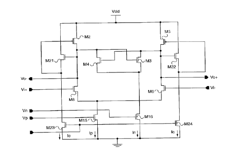
The delay element according to the invention is depicted in Figure 1 The
diagram
therein is substantially identical to the one described in the above cited
document by B.
Razavi (see in particular Figure 35) and differs in the way the bias of the
load and
feedback transistors is obtained, that is a particular feature of the
invention and results
in a wider tunability range.
That being stated, the delay element comprises a conventional differential
amplifier formed by the transistors M8, M6, M15 (of N type) and M2, M5 (of P
type), in
which the two P transistors form the load.
The signal to be delayed is applied to the gates of the two transistors M6, M8
(Vi-
and Vi+, respectively) and the output voltage is present at the point common
to the
drains of the transistors M5, M6 and M2, M8 (Vo- and Vo+, respectively).
Transistor
M1 Ei is the bias transistor of the amplifier arid a variable control voltage
is applied to its
gatE: and generates a variable drain current Ip which when added 1:o a
variable current
In supplied by a pair of feedback transistors> M3, M4, represents the bias
current of the
differential stage (in particular the bias current of the load transistors).
The feedback -transistors M3, M4 (they, too, of N type) have their gates
connected to the drains of Ma and M2, respectively, and form a negative
impedance
Z2 which is set in parallel to the load transistors M2, M5. The two
transistors M3, M4
are biased by a transistor M16, to the gate of which a variable control
voltage Vn is
applied which originates the variable drain current In forming the bias
current of
feedback transistors M3, M4.
Additionally, the load transistors M2, M5 are associated to rEapective
transistors
M2~ . M22, biased by the transistors M23, M24, which implement two source
follower
stages. The latter transistors have the task of correctly biasing the gates of
load
transistors M2, M5, thus reproducing at the gates of these transistors the
same voltage
CA 02290723 2003-04-07
variations as those occurring at their drains, but with a lower rest voltage,
in order to
increase the upper limit of the output voltage up to a value almost equal to
the power
supply voltage, without affecting the correct operation of the sy.>tem.
Reference Ic
denotes the drain current of the transistors M23, M24 (bias currenl of
transistors M21,
M22~ of the source follower stages) obtained starting from a control voltage
Vc applied
to the gate of M23, M24.
According to the invention, in order to extend the delay (or frequency)
tunability
range, in addition to causing the variation of Ip, In, also bias current Ic of
transistors
M21, M22 (drain current of M23 or M24} is caused to vary, in such a way as to
L0 increase as the delay decreases. Furthermore, the modulation of the
currents Ip, In is
no longer effected starting from a common control voltage (as in thf: known
technique),
but in an independent way, so that the surn of the current in the feedback
transistors
and in the load transistors linearly increases and is no longer constant (i.e.
there is no
longer a symmetrical sharing between the N transistors and the P transistors).
IS Therefore, transistors M21, M22 are nc longer used as simf>le source
follower
elements, as in the known technique, but they take part in the tuning of the
delay,
according to the process explained in the sequel.
In other terms, the invention aims at to making the impedance of load
transistors
M2, M5 vary in such a way as to cause a reduction of the delay. For such a
purpose
20 the control current Ic is caused to increase by reducing said impedance.
Further, to
prevent the circuit gain from decreasing as the impedance of i:he load
transistors
decreases, current Ip is increased so as to recover the gain constancy
conditions. The
increase in Ip is further conducive to a reduction of the impedance and
therefore of the
delay.
25 The current values obtained through the bias modalities according to the
invention exhibit the behaviour depicted in Figure 2. In said Figure, the
ordinates show
the value of Ip, In, Ic (in pA). The abscissa gives in arbitrary units the
value of a control
signal allowing the circuit in which the delay element is used to run over the
whole
tuning range (in the present case, a signal from which the three voltages Vp,
Vn, Vc
30 can be derived). The minimum abscissa corresponds to the maximum delay (and
therefore to the lowest oscillation frequency, in the event of use in an
oscillator).
The diagram of Figure 2 shows, if cc>mpar~d with the corresponding diagram of
Figure 3 relating to the known technique (where the sum of currents In, Ip and
control
current Ic is constant) that the invention guarantees at least a considerable
downward
35 extension of the variability range of the delay (and therefore an upward
extension of
the range of frequency tunability), by virtue of the joint increase of Ip and
Ic and
therefore of the decrease of the impedance Z1 of the load transistors. As
already
CA 02290723 2003-04-07
previously stated, given the source follower connection between transistors
M21 and
M22 (or M2 and M5), the increase of current Ic of transistors M21, M22 causes
the
incrE:ase in the gate-source voltage Vgs of transistors M2, M5: as <~
consequence, the
transconductanc:es of the same transistors increase, and their impedance Z1
decreases, and therefore the delay decreases. Since there is no longer the
constraint
imposed by the uniform sharing of Ip and In between the load transistors M2,
M5 and
the feedback transistors M21, M22, the increase in Ip can occur more rapidly
than the
decrease in Ip. The above situation occurs, provided the negative impedance Z2
is
much higher in absolute value, and this is obtained for the reason that
current In in the
feedback stage decreases as Ic increase:y. A reduction in Z-1 hE~lps in
keeping the
stability condition (Z1 < IZ21).
Furthermore, with reference to the application to a ring oscillator, which at
present represents the preferred application, since the amplitude c>f the
oscillations is
given by the product of the total current flowing through the load transistor
and the
impedance of the same, it becomes evident that the increase in Ic and the
consequent
decrease in Z1, ensure the constancy of amplitude of the oscillation as the
frequency
increases.
Suitable variation ranges for currents Ic, In, Ip, can be the folic>wing:
Ic: 3 to 10 frA as minimum value, 50 to 100 ~iA as maximum value;
Ip: 5 to 15 NA as minimum value, 220 to 350 NA as maximum value;
In: 90 to 150 ErA as maximum value, 0 irA as minimum value.
Tests performed on a ring oscillator using four delay elements biased
according
to the invention have proven that the tunability range which can be guaranteed
has an
amplitude equal to 6-7 times the minimum frequency, thus much higher than the
one
which can be obtained according h~ the known technique. In practical exemplary
embodiments, minimum frequencies between approximately 0.22 GHz (fast N
transistors and typical P transistors) and approximately 0.4 GHz (typical N
transistors
and fast P transistors, or slow N transistors and typical P transistors), and
maximum
frequencies between approximately 2 c~aHz (slow N and F' transistors) and
approximately 3GHz (typical N transistors and fast P transistors) have been
achieved.
For comparison, an identical oscillator using delay elements according to the
known
technique exhibited minimum frequencies between 0.5GHz and 1 GHz and maximum
frequencies between 1.1 GHz and 1.E~ GHz. These tests prove that the invention
allows
not only the up-extension of the frequency tunability range in an oscillator
in which is
adopted, as shown in Figure 2, but also an extension in the oppositE:
direction.
As a matter of fact, in the lower part of the tunability range, the
transistors M21,
M22 mounted according to the known technique (i.e. as sheer source follower
CA 02290723 1999-11-25
6
elements) were biased statically as a trade-off between the maximum delay and
the minimum
delay obtainable, whereas according to the invention the bias variation
according to the
method already illustrated, allows its contribution to the tunability range,
which is therefore
extended both upwards and downwards.
Its is evident that what has been described is only given by way of a non
limiting
example and that variations and modifications are possible without departing
from the
scope of the invention. In particular, even if a decrease in the delay has
been discussed in
more details in the specification, a delay increase can be performed: this
requires the
opposite variations of the bias currents.