Note: Descriptions are shown in the official language in which they were submitted.
CA 02290819 1999-11-19
WO 98/53499 PCT/IL98/00230
-1
" SUBSTRATE FOR ELECTRONIC PACKAGING,
PIN JIG FIXTURE
FIELD OF THE INVENTION
This invention relates to substrates for electronic packaging including
inter alia ball grid array packaging (BGA), chip size/scale packaging (CSP)
and mufti-chip/module packaging (MCP/MCM), and a process of
manufacturing therefor. In addition, the invention relates to a fixture for
masking purposes, and a process using the fixture for preparing a selectively
patterned valve metal surface.
BACKGROUND OF THE INVENTION
Conventional electronic packaging includes a discrete substrate on
t 0 which one or more integrated circuit chips (ICCs) are mounted on its
topside,
for example, in the case of BGA, as illustrated and described in US Patent
No. 5,355,283 to Marrs et al. The discrete substrate can be of a wide range of
materials including ihter alia aluminum and irrespective of its material,
through holes are drilled between its topside and underside. In the case of an
t 5 aluminum substrate, each hole is initially anodized to create an
insulating
" sleeve prior to the insertion of a metal pin, thereby enabling electrical
and
thermal communication between its topside and underside.
Depending on the intended complexity of an electronic package, a
mufti-layer interconnect structure can be interdisposed between the ICCs and
CA 02290819 1999-11-19
WO 98/53499 PCT/IL98/00230
.2.
the substrate, for example, as illustrated and described in US Patent No.
5,661,341 to Neftin. Such a multi-layer interconnect structure has one or
more aluminum layers, each layer being deposited on a previously prepared
topside and typically having a thickness in the order of between about O.Sl,un
S and about 20~xn.
Conventional masking for area selective anodization purposes is a
relatively complicated and expensive process including the application and
subsequent removal of an inert masking layer using photolithography and
deposition techniques, the layer being in the form of a photoresist material,
a
dense oxide layer, a tantalum metal thin film, and the like.
SUMMARY OF THE INVENTION
In accordance with a first aspect of the present invention, there is
provided a substrate for electronic packaging, the substrate comprising a
discrete, generally prismatoid, initially electrically conductive valve metal
t 5 solid body with a pair of opposing major surfaces, said body having one or
more original valve metal filled vias substantially perpendicular to said
major
surfaces, said filled vias being spaced apart and individually electrically
isolated by a porous oxidized body portion therearound.
A substrate in accordance with the present invention can be fabricated
from suitable valve metal blanks of aluminum, titanium, or tantalum, and
preferably inter alia AI 5052, A1 5083, Al 1100, Al 1145, and the like. Such a
substrate can be readily manufactured to customer requirements in terms of a
desired filled via pattern; electrical properties; the relative proportions of
the
original valve metal filled vias and the porous oxidized body portions;
thermo-mechanical properties such as thermal coefficient of expansion
(TCE), substrate strength, Young modulus, elasticity; thermal properties such
as thermal conductivity coe~cient; and other factors. Such a substrate can be
manufactured with a minimum filled via diameter of about 25~"anm and a
CA 02290819 1999-11-19
WO 98/53499 PCTIIL98/00230
-3
minimum center to center distance between adjacent filled vias of about 50
E,,~m, thereby affording high miniturization and high frequency operation of
' electronic packaging.
In accordance with a second aspect of the present invention, there is
provided a process for manufacturing a discrete substrate for electronic
packaging, the process comprising the steps of
{a) providing a discrete, generally prismatoid, initially electrically
conductive valve metal, solid blank having a pair of opposing
major surfaces, the blank having a plurality of spaced apart
t 0 generally cylindrical through sections, each through section
having end surfaces and extending substantially perpendicular
to the pair of opposing major surfaces;
(b) selectively masking both end surfaces of one or more of the
through sections; and
t 5 (c) porously oxidizing the blank whereupon a porous oxidized
portion forms around a through section whose both end
surfaces are masked thereby retaining the through section as an
original metal valve filled via.
A process of manufacturing a discrete substrate for electronic
20 packaging in accordance with the present invention involves a low number of
steps and is suitable for large area panel production. During or post
anodization, suitable materials can be impregnated into the blank's oxidized
portions which typically thicken and therefore require planarization to
restore
them to their original thickness.
25 The porous anodization can be either one- or two-sided depending on
the thickness of the generally cylindrical through sections some of which are
to be retained as original valve metal filled vias. Typically, one-sided
porous
anodization can be applied to a maximum through section thickness of about
150 Nln whilst two-sided porous anodization can be applied to a maximum
CA 02290819 1999-11-19
WO 98153499 PCT/IL98/00230
-4
through section thickness of about 300 pxrl. One- and two-sided porous
anodization can be effected in a conventional manner, for example, as
illustrated and described in US Patent No. 5,661,341 to Neftin.
In accordance with a third aspect of the present invention, there is
provided a pin jig fixture for mechanically masking a valve metal surface, the
pin jig fixture comprising an anodization resistant bed of pins each having a
leading end surface for intimate juxtaposition against a portion of the metal
surface whereby said portion is masked.
A pin jig fixture in accordance with the present invention enables the
simultaneous masking of one or more portions of a valve metal surface by its
mechanical clamping thereagainst. Typically, the pins have planar end
surfaces which are co-planar, however, a jig pin fixture can have pins of
different lengths whereby their end surfaces lie on different parallel planes.
The bed of pins can be fabricated from any suitable anodization resistant
material including ceramics, valve metals, and the like.
The pin jig fixture can be preferably employed to directly oxidize
those non-masked portions immediately surrounding the metal surface
portions masked thereby, in which case, the pins are fabricated from valve
metal and have electrically conductive end surfaces connectable to a power
source. In addition, the pin jig fixture advantageously negates the need for
an
otherwise redundant portion of a substrate, such portion conventionally being
initially used for connection to an electrical source and which is
subsequently
removed.
In accordance with a fourth aspect of the present invention, there is
provided a process for preparing a selectively patterned valve metal surface,
the process comprising the steps of-.
(a) providing a pin jig fixture having an anodization resistant bed
of pins each having a leading end surface;
CA 02290819 1999-11-19
WO 98/53499 PCT/IL98/00230
-5
(b) intimately juxtaposing leading end surfaces against a valve
metal surface to mask portions thereof; and
(c) anodizing the masked metal surface.
BRIEF DESCRIPTION OF THE DRAWINGS
In order to understand the invention and to see how it may be carried
out in practice, preferred embodiments will now be described, by way of
non-limiting examples only, with reference to the accompanying drawings, in
which:
Fig. 1 is a pictorial view of a finished discrete aluminum substrate in
accordance with a first embodiment of the present invention;
Fig. 2 is a cross section view of the substrate of Figure 1 along line
A-A;
Fig. 3 is a pictorial view showing the porous oxidization of a blank
during the manufacture of the substrate of Figure 1;
Figs. 4-6 correspond to Figures 1-3 for a finished discrete aluminum
substrate in accordance with a second embodiment of the present invention;
Figs. 7-9 correspond to Figures 1-3 for a finished discrete aluminum
substrate in accordance with a third embodiment of the present invention;
Figs. 10-12 correspond to Figures 1-3 for a finished discrete aluminum
substrate in accordance with a fourth embodiment of the present invention;
Fig. 13 is a perspective view of a pin jig fixture in accordance with the
present invention;
Fig. 14 is a cross section view of the pin jig fixture of Figure 13 along
line E-E; and
Fig. 15 is a side view showing the mechanical clamping of a substrate
by two pin jig fixtures of Fixture 13.
CA 02290819 1999-11-19
'. ..
.. ~ . .
i i " ' . i ~r . ' '
'
. . 1. . . '
".
' ' ; . ' ' ' : ~
' i ' ' ' '. ..
~
..
" .'
'
'.'
-6-
DETAILED DESCRIP'ITON OF THE DRAWIrtGS
In the drawings, different materials during the process of manufacturing a
device of the present invention are shown in different shading, the different
s materials including aluminum metal, porous aluminum oxide, and a mask. In
addition, porous anodization is illustrated by arrows with curly tails.
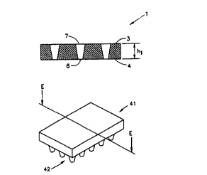
With reference now to Figures 1-3, a device 1 for use as a BGA support
structure, an MCM support structure, a CSP support structure and the like has
a
discrete solid body 2 with opposing generally parallel major surfaces 3 and 4.
1o The solid body 2 has a sealed or unsealed porous aluminum oxide body
portion 6
with a pair of exterior surfaces 7 and 8 constituting portions of the major
surfaces
3 and 4, respectively. The body portion 6 has an array of one or more
electrically
insulated inverted frusto-conical aluminum vial 9 embedded therein. Each
aluminum via 11 constitutes an electrically insulated original valve metal
15 conductive trace and has exterior surfaces 12 and 13 constituting portions
of the
major surfaces 3 and 4, respectively. The device 1 is manufactured from an
aluminum blank 14 with a full mask 16 applied to its major surface 3 and an
array
17 of circular masking elements 18 corresponding to the array of aluminum vial
9 applied to its major surface 4 prior to its undergoing one stage one-sided
porous
2o anodization. A typical device 1 has the following specification: h = 100
Vin, b =
300 Vin, di = 75 pm, and d2 =150 E,irn.
Turning now to Figures 4-6, a device 21 is similar to the device 1 of
Figure 1 and differs therefrom in that it is thicker and has an array of one
or more
barrel shaped aluminum vial 22, namely, each aluminum via 23 initially
diverges
2s and thereafter converges from an exterior surface 24 constituting a portion
of the
major surface 3 to an exterior surface 26 constituting a portion of the major
surface 4. The device 21 is manufactured from an aluminum blank 27 with two
identical arrays 17 applied to its major surfaces 3 and 4 prior to its
undergoing
9N~~C»iD~ <E~~. 9892~705!XJ>
-......_.._ . _..
CA 02290819 1999-11-19
, ,.
f
f f ~ ~ ,
..
. ~ a f
, , ..
~ ~ ~ ~
~ ..
' .
..
-7-
one stage dual-sided porous anodization. A typical device 21 has the following
specification: h = 200 pm, b = 0.3 mm, dl =120 ~,un, and d2 =150 Eon.
Turning now to Figures 7-9, a device 28 is similar to the device 1 of
Figure .1 and differs therefrom in that it manufactured from an aluminum blank
29 having an array of thin regions 31, each thin region 32 being atop a
frusto-conical shaped recess 33. The aluminum blank 29 undergoes one stage
one-sided porous anodization in a similar fashion to the aluminum blank 14 of
Figure 3 so as to form an array of aluminum vias 9 in the thin regions 32 and -
-
whereby electrically insulated aluminum pockets 34 are also formed. A typical
to device 28 has the following specification: hi = 500 Vim, h2 = 100 E,un, b =
1000
~xn, dl = I00 Wtn, and d2 = 150 Eon.
Turning now to Figures 10-12, a device 36 is similar to the device 28 of
Figure 7 and differs therefrom in that it has thicker thin portions 32 thereby
requiring one stage dual-sided porous anodization in a similar fashion to the
1s blank 27 of Figure 6 which leads to an array of barrel-shaped aluminum vial
22.
A typical device 36 has the following specification: hl = 500 E,om, hZ = 200
E,im, b
=1000 E.un, dl = 150 ~, and d2 = 200 pm.
Turning now to Figures 13-15, a pin jig fixture 121 for use with an
electrical power source (PS) 122 for porous anodization of a valve metal blank
20 123 with a surface 124 includes a bed of cone shaped pins 126. The bed of
pins
126 is made from titanium and is directly connected to the power source 122.
Each pin 127 has a leading end surface 128 for intimate juxtaposition against
the
surface 124 for connection of the blank 123 to the power source 122. Doting
porous anodization, all the underside surface of the pin jig fixture 121
including
2s the peripheral surfaces 129 of the pins 127 is converted into dense
titanium oxide
whilst all its interior including the cores 131 of the pins 127 remain
titanium such
that the pin jig fixture I21 is suitable for multiple porous anodizations.
A single pin jig fixture 121 can be employed in one-sided porous
anodization, for example, to selectively pattern aluminum blanks 14 and 27 in
the
~lSf~~,r,W :FW co~~7r~r!Y'~~
CA 02290819 1999-11-19
_ a. ..
~ ~' ~. ~ ~ ~ ~ " '
~~ ~ ~ ~~ ~ ~ ~
~ s' . ~ ~ ~ ~ ~ ~'~ ~..
~ ~ ~ ~ ~ ~ ~
~ ~ ~ . ~ ~
~
~ ~ ~~~ ~' .~ ~~ ~~ .~
manufacture of discrete aluminum substrates 1 and 28, respectively. Or a pair
of
fact-to-face pin jig fixtures 121 can be employed in two-sided porous
anodization, for example, to selectively pattern aluminum blank 29 in the
manufacture of discrete aluminum substrates 21 and 36, respectively.
While the invention has been described with respect to a limited number
of embodiments, it will be appreciated that many variations, modifications,
and
other applications of the invention can be made.
Pei.rrr~r~n..r1 Oclo~7n5(W..
~ _.__ .. ... _'y....