Note: Descriptions are shown in the official language in which they were submitted.
CA 02290965 1999-11-23
WO 98/58411 PCT/GB98/O1'734
_~_
PHOTODETECTOR CIRCUIT
This invention relates to a photodetector circuit.
Semiconductor photodetectors based on the silicon bandgap are suitable for
operation in the visible and near infrared region of the spectrum. Prior art
silicon
photodetectors can be constructed in compact form and cheaply using mature
CMOS technology. Photon illumination of a photodiode results in the generation
of
an electrical current, the photocurrent. It is desirable for many applications
for the
photodetector to be responsive to a very wide range of input intensities. This
is
facilitated by passing the photocurrent through a MOSFET load device operating
in
its subthreshold regime. In this regime, MOSFET output (voltage) response is a
logarithmic function of its input (current). Thus the combined
photodiode/MOSFET
device has a logarithmic illumination versus output voltage characteristic.
The
dynamic range of the overall system is very large: detectable illumination may
vary
by as much as 5 or 6 orders of magnitude.
A problem with such prior art devices is that the MOSFETs have inherent
leakage
currents which represent a substantially constant loss in a stable
environment.
There are two consequences of this leakage current which significantly limit
conditions under which such CMOS photodetecting circuits can be operated
effectively. First, although leakage current is not a significant problem in
high
illumination intensity when the MOSFET is operated at current levels far
larger than
the leakage level, it can severely degrade detector sensitivity at low light
levels.
Secondly, leakage current is highly temperature dependent and increases
severely
at elevated temperatures. While the first of these problems has been widely
addressed in the prior art, the second has received little attention.
Very low fight sensitivity has been improved by moving from pure CMOS to
parasitic
bipolar circuitry within a CMOS process. For example, Mead in Analog VLSI and
Neural Systems, Addison-Wesley 1989, p218 - 219 and p260 - 261, describes such
' a photodetector circuit. The photodiode is replaced with a bipolar
transistor with gain
(3. This amplification characteristic raises the low level visibility
"approximately to a
moonlit scene focused on the chip through a standard camera lens". However,
CA 02290965 1999-11-23
WO 98158411 PCTIGB98/01734
-2-
where low tight levels are of particular interest, problems still remain. For
example,
US patent 5 097 305 to Mead addresses this problem. Mead discloses a
phototransistor whose photocurrent is, following the usual practice, read
instantaneously at higher values, but readout charge is integrated at the low
end of
the photocurrent scale. Similarly, US patent 5 155 353 to Pahr, is concerned
with
reducing the susceptibility to noise of photodetector circuits employing
either
phototransistors or photodiodes, which again is more problematic at low-light
levels.
Thus, while these phototransistor circuits may have some specialist
applications, the
fact remains that the cheaper and more compact pure CMOS devices work
acceptably well down to twilight illumination levels and the adaptation is not
generally worthwhile.
A more fundamental obstacle to the general portability of CMOS photodetectors
is
their temperature instability, noted above. This is potentially a serious
barrier to the
commercial uptake of CMOS detectors in instruments designed to respond to
everyday light levels, such as the recently developed digital cameras. This is
despite the inherent cost and performance advantage offered by CMOS over
currently used CCD detectors. There is a perceived market for a single camera
which operates effectively in the variety of environments and throughout the
whole
range of illumination levels to be anticipated by the modern photographer.
The low-light sensitivity of pure CMOS photodetectors has been improved by
operating at tow temperatures and exploiting the consequent reduction in
leakage
cun-ent. However cooling apparatus e.g. Pettier cooler or dewar, is bulky and
represents a significant drain on power sources, proving inconvenient to
numerous
applications.
It is the object of this invention to provide a photodetector with improved
temperature
stability.
The present invention provides a substantially temperature-insensitive
photodetector
circuit characterised in that it incorporates photon detecting means arranged
to
produce an electric current in response to incident photon illumination
associated
CA 02290965 1999-11-23
WO 98/5841 I PCT/GB98/01734
-3~
with a current load device arranged to produce a voltage response to current
flow
wherein
(a) the photon detecting means is arranged to provide an output current which
is
supplied to the current load device,
. 5 (b) the current load device has a current-voltage characteristic in which
the voltage
is a logarithmic function of current flow, and
(c) the photon detecting means is a phototransistor with a current gain factor
greater than unity.
In an alternative aspect, this invention provides a photodetector circuit
incorporating
photon detecting means arranged to produce an electric current in response to
incident photon illumination associated with a current load device arranged to
produce a voltage response to current flow wherein
(a) the photon detecting means is arranged to provide an output current which
is
supplied to the current load device,
(b) the current load device has a current-voltage characteristic in which the
voltage
is a logarithmic function of current flow,
(c) the photon detecting means is a phototransistor with a current gain factor
greater than unity, and
(d) the circuit is substantially insensitive to temperature over a range of
light
intensity and temperature normally to be encountered in a daytime natural
environment.
This invention provides the advantage of improved temperature stability
compared to
prior art photodetecting devices which are also capable of responding to a
large
dynamic range of incident illumination intensities. The gain of the
phototransistor
acts on the generated photocurrent to produce a far larger output current in
comparison with that generated by a comparable p-n photodiode. This
amplification
of the current supplied to the current load device ensures that current within
the load
is generally much higher than the leakage current, even at elevated
temperatures
and yet still maintains the load logarithmic voltage response. Leakage current
therefore represents only a small loss from the perceived photocurrent and
accurate
intensity measurements of normal illumination levels can be made at relatively
high
temperature.
CA 02290965 1999-11-23
WO 98/58411 PCT/GB98101734
-4-
The invention also, as an additional effect, improves the low-illumination
level
response of a photodetector circuit in comparison with CMOS circuitry. This is
in
contrast to prior art disclosures in which the actual sought after effect is
extension of
the low illumination limit of CMOS. A further, inherent, advantage arises in
improving temperature stability in the manner of this invention, which is
improvement
in signal to noise ratio. A major contribution to noise depends on charge
carrier
concentration and therefore also on magnitude of leakage current; signal to
noise
ratio is degraded by an increase in leakage current, but it is improved if the
signal is
amplified above the leakage current level in accordance with the invention.
This invention has numerous applications to imaging objects used in everyday
environments, which can typically be expected to vary in temperature. In a
particularly preferred embodiment, the invention is incorporated in a digital
camera,
of the kind now becoming ever more popular despite the disadvantages of CCD
detectors currently used therein. Modern day travellers expect such a camera
to last
a number of trips, and to serve them well across a variety of temperature and
light
conditions They require a lightweight camera capable of imaging acceptably all
areas of a scene at temperature extremes in both hot and cold climates.
Specifically, the phototransistor and current load device may be arranged to
provide
an output signal including a contribution from leakage current and a
contribution
responsive to incident illumination and the latter contribution exceeds the
former at
all normal operating temperatures of the circuit such that the circuit is
substantially
temperature-insensitive.
In a preferred embodiment, the phototransistor and current load device are
fabricated using BiCMOS technology. BiCMOS is an optimised technology covering
fabrication of both bipolar and CMOS devices which thus gives the advantage of
versatility. The phototransistor and load device may therefore bt f any type
(e.g.
FET, npn, pnp, etc.), and fabricated in the same process. Other considerations
may
thus be taken into account in specific applications in order to determine the
most
appropriate implementation of this embodiment of the invention.
CA 02290965 1999-11-23
WO 98/58411 PCT/GB98/01734
~5-
The current load device may be a MOSFET device with its source or drain
connected to the phototransistor and the phototransistor is an-anged to
produce an
. electric current which is low enough to operate the MOSFET in its
subthreshold
regime. This provides the advantage of economy. A MOSFET operating
subthreshold provides the desired logarithmic output with which to extend the
dynamic range of a photodiode or phototransistor. The MOSFET can be fabricated
using CMOS technology, the state of which is such as to permit relatively
cheap
fabrication.
The phototransistor is preferably a bipolar transistor incorporating a
photodetecting
base region and with emitter connected to the load MOSFET. Such a bipolar
phototransistor provides the required photosensitivity and has high
amplification: the
output current can be larger by a factor of ~ 100 in comparison with a p-n
junction
photocurrent. FET phototransistors do not generally exhibit the same degree of
gain
and therefore cannot raise the signal above the transistor leakage level over
such a
wide temperature range. Furthermore a bipolar transistor may provide the
advantage that the circuit is relatively easily fabricated. Such transistors
may be
manufactured in CMOS as a natural by-product of the bulk process. Generally,
these lateral or vertical bipolar transistors are considered parasitic, as
they may lead
to problems in standard logic circuits. However, their photodetecting
capability
makes them ideally suited to this application.
In an alternative aspect, this invention provides a substantially temperature-
insensitive photodetector circuit characterised in that it includes a bipolar
phototransistor, a load MOSFET and voltage detecting means wherein:
(a) the bipolar phototransistor is arranged to supply photocun-ent output to
the load
MOSFET,
(b) the phototransistor is arranged such that photocurrent output is
sufficiently small
to maintain subthreshold operation of the load MOSFET, and
- 30 (c) voltage detecting means is arranged to detect a voltage output from
the load
MOSFET in response to photocurrent supply.
In a preferred embodiment, the phototransistor and current load device are
fabricated using BiCMOS technology.
CA 02290965 1999-11-23
WO 98/58411 PCTlGB98/01734
-6~
As noted above, bipolar phototransistors may result from the CMOS fabrication
process as parasitic devices. However, this is not ideal as such devices are
not
optimised on a standard CMOS process. Although they may be suitable for some
applications, these bipolar phototransistors are large and have low matching.
The
former feature forces the detector designer to accept either poor pixel
spatial
resolution or an expensive requirement for a physically large array. The
latter
feature leads to high fixed pattern noise. However, as a fabrication process,
BiCMOS provides the advantage that it affords a compromise between these
extremes. BiCMOS is optimised both for CMOS and bipolar device manufacture,
making it eminently suitable for application to devices requiring both device
types.
When compared with parasitic bipolar technology therefore BiCMOS provides the
advantages of higher spatial resolution and reduced fixed pattern noise. Fixed
pattern noise arises in array circuits in which the response characteristics
of
individual circuit elements differ across the array {low matching). This
introduces a
noise level caused by unequal responses to the same illumination. However
bipolar
transistors can be fabricated more uniformly in BiCMOS, giving rise to a
reduction in
fixed pattern noise.
Furthermore, BiCMOS allows the readout circuit to be made with lower noise
that an
equivalent CMOS circuit, thus increasing the performance of the photodetecting
system still further.
Specifically, the photodetector may be for the purpose of operation in
environmental
temperatures ranging from -20 to 60°C with substantially unaffected
sensitivity at
illumination levels down to 1 lux. This provides the advantage that the
detector is
suitable for application in most natural conditions of illumination and
temperature.
The photodetector circuit may incorporate an attenuator arranged to reduce the
intensity of light prior to incidence on the phot~n detecting means to an
extent
necessary to provide for the resultant output current to be low enough to
operate the
MOSFET in its subthreshold regime. This provides the advantage of flexibility.
The
upper end of the phototransistor dynamic range may, in high-illumination
situations,
result in a photocurrent sufficiently large that it pushes the MOSFET out of
its
CA 02290965 1999-11-23
WO 98158411 PCT/GB98/01734
_~~
saturation regime, and the logarithmic response of the circuit will be lost.
The use of
an attenuator guards against this eventuality.
In particular, the photodetector may be capable of operation in environmental
temperatures ranging from -20 to 60°C with substantially constant
contrast
sensitivity.
In a preferred embodiment the load MOSFET and phototransistor are connected at
a
common connection point to buffering means and the buffering means is
connected
to a pixel readout circuit.
The photodetector circuit may be incorporated in an array of like circuits.
This
provides the advantages generally to be had from an array of imaging pixels.
Alternatively, an embodiment of the invention provides a detector array of
photodetector circuits each of which may be in accordance with an aspect or
embodiment described above.
A further embodiment provides a digital camera incorporating an array of
photodetector circuits each of which may be in accordance with an aspect or
embodiment of the invention described herein.
A further aspect of this invention provides a digital camera incorporating an
array of
photodetector circuits characterised in that each circuit incorporates photon
detecting means arranged to produce an electric current in response to
incident
photon illumination associated with a current load device arranged to produce
a
voltage response to current flow, and wherein
(a) each circuit is of BiCMOS construction,
(b) the photon detecting means is arranged to provide an output current which
is
supplied to the current load device,
(c} the current load device has a current-voltage characteristic in which the
voltage
is a togarithmic function of current flow,
(d} the photon detecting means is a phototransistor with a current gain factor
greater than unity, and
CA 02290965 1999-11-23
WO 98/58411 PCT/GB98101734
_g_
(e) the phototransistor and current load device are arranged to provide an
output
signal including a contribution from leakage current and a contribution
responsive to incident illumination and the latter contribution exceeds the
former
at all normal operating temperatures of the circuit such that the circuit is
substantially temperature-insensitive.
Further embodiments of this invention may provide an apparatus comprising hand
held computer technology or a personal digital assistant incorporating an
array of
photodetector circuits each in accordance with an aspect or embodiment of the
invention described herein.
With developing technology, digital cameras are being included in a number of
compact devices. For example personal digital assistants ("pda"s or "palm top
computers") often incorporate such a camera to increase their functionality.
Clearly,
to increase portability without losing functionality it is desirable to have
as compact
and as lightweight an imaging system as possible. Furthermore, many users will
travel with their pda, which could be essential to their business concerns.
There is
thus a requirement that the imaging function of such devices will operate
effectively
over a range of world temperatures and climates.
A car may incorporate a digital camera and signal processing means wherein the
signal processing means is arranged to analyse data received from the digital
camera and assist in car control. This is advantageous to safe driving. The
digital
camera may be installed next to a car driver and used to provide, for example,
advanced cruise control. The camera can be set up to detect, for example,
another
car pulling out in front. The signal processing can then be arranged to
respond to
the hazard and control the car (for example, apply the brakes) accordingly.
Of primary importance to any such safety mechanism is that it can be relied
upon at
aN times. Thus, although a stable temperature will be reached after some time
driving, it is necessary to ensure that the imaging capability is adequate at
start up.
Cars may be, and often are, parked in a variety of weather conditions and the
temperature can consequently be very hot, very cold or anywhere intermediate
these
extremes at start up. By using a digital camera incorporating the temperature-
CA 02290965 1999-11-23
WO 98/58411 PCT/GB98/01734
-9~
insensitive photodetector circuit of this invention, reliable operation over
the required
temperature range can be achieved.
In another aspect, this invention provides a substantially temperature-
insensitive
method of measuring photon radiation intensity over a dynamic range greater
than
four orders of magnitude characterised in that the method comprises the steps
of:
(a) providing a photodetector circuit comprising a bipolar phototransistor
arranged
to supply output current to a load MOSFET,
(b) arranging the phototransistor to respond to incident radiation by
providing output
current to operate the load MOSFET subthreshold,
(c) detecting the load MOSFET output voltage response to said output current.
Preferably, the photodetector circuit of Step (a) is fabricated in BiCMOS.
In order that the invention might be more fully understood, an embodiment
thereof
will now be described with reference to the accompanying drawings in which:
Figure 7 is a circuit diagram of a prior art photodetector pixel.
Figure 2 is circuit diagram of a photodetector pixel of the invention.
Figure 3 is a schematic illustration of a digital camera incorporating an
array of
photodetector pixels of the invention.
With reference to Figure 7, a pixel of a prior art photodetector circuit is
illustrated
generally by 10. This photodetector pixel 10 is suitable for incorporation in
an array
of like pixels to create a detector array. The photodetector pixel 10
comprises a
photodiode 12 and load metal oxide field effect transistor (MOSFET) 14
connected
via MOSFET source 16 at connection node 18. The MOSFET 14 also has drain
connected to both gate and power supply VDO and therefore constitutes a load
for
the photodiode 12. In this arrangement light 20 incident on the photodiode 12
results in a photocurrent !~, and voltage Vp,, being developed at the
connection 18.
This connection 18 is buffered from a constant current sink (not shown) by a
second
MOSFET 22. The second MOSFET 22 has gate 24 connected to the connection 18,
CA 02290965 1999-11-23
WO 98/58411 PCT/GB98/01734
~10-
drain 26 connected to the power supply Vop and source 28 to a MOSFET switch
30.
It thus constitutes a source-follower driver. A switch voltage (VS"") may be
applied to
a MOSFET gate 32 in order to operate the MOSFET switch 30. This provides for
an
output voltage ( Vo"r) to develop at a pixel output line 34 which is connected
to an
array readout circuit (not shown).
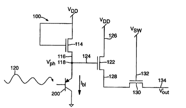
Figure 2 illustrates a photodetector pixel circuit of the invention, indicated
generally
by 100. This photodetector pixel 100 comprises a number of components which
are
common to the prior art device 10. Such components are referenced by numbers
100 greater than the corresponding references in Figun? 1 and include: a load
MOSFET 114 with source 116 connected to connection node 118 and drain and
gate connected as for Figure 1; second MOSFET 122 with gate 124, drain 126 and
source 128 connected as for Figure 1; switching MOSFET 130 addressed via its
gate 132; and pixel output line 134. The photodetector pixel of the invention
100
also includes a bipolar phototransistor 200. The bipolar phototransistor 200
has its
emitter connected to connection node 118.
With reference to Figure 1, the operation of the prior art photodetector pixel
10 will
now be described. Light 20 incident on the photodiode 12 results in the
generation
of photocurrent Ip,,. This current is constrained to flow as the source-drain
current of
the load MOSFET 14 by virtue of its isolation from the remainder of the
circuit by the
second MOSFET 22. A fraction of this photocurrent is however lost from the
MOSFET 14 as a leakage current l~ke~, and the MOSFET 14 actually operates at
an input channel current I~,,. In consequence of this channel current 1~,,, a
voltage
difference ( VgS) develops between gate and source of the load MOSFET 14 to
the
extent necessary to operate the load MOSFET 14 at this current I~,,. This
voltage
difference V9S is attained by driving a voltage at the MOSFET source 16 to a
value
Vp,, (-VDO - Vgs). This voltage Vp,, is therefore that appearing on the
connection node
18, which contains information regarding illumination intensity and which is
consequently termed the photovoltage. The photodetector 12 is constructed such
that over a range of expected illumination intensities, the generated
photocurrent
(lp,,) is much less than that needed to drive the voltage difference VgS above
the load
MOSFET threshafd voltage. The MOSFET 14 therefore operates in its subthreshold
regime. In this regime, a MOSFET drain current (Id) is an exponential function
of its
CA 02290965 1999-11-23
WO 98158411 PCT/GB98/01734
-11-
gate-source voltage difference (VAS) and therefore also of its source voltage
(VS):
Id ~c exp (V$). In the photodetector circuit 10, the gate voltage is held at
Voo and the
source voltage is the photovoltage V~, developed at connection 18. The drain
current is the channel current l~n, and so:
I~h oc exp ( V~,)
_> Vp,, oc In l~n
and VP,, oc In {Ipn - I~x~)
Thus, if the leakage current is negligible in comparison with the generated
photocurrent, the photovoltage is proportional to the logarithm of the
photocurrent
response: V~,, ~c In Iw,.
The voltage V~, generated at connection 18 is applied to the gate 24 of the
second
MOSFET 22. The drain-source current of this MOSFET 22 is constant, constrained
by the constant current sink. The voltage {Vsr) at the source 28 of this
MOSFET 22
therefore follows any variation in the gate voltage (photovoltage Vpn) in
order to
maintain this constant current. The MOSFET 22 thus functions as a source-
follower
driver: VS, = VPn - O, where O is the voltage drop required to operate the
MOSFET at
the current provided by the constant current sink. This MOSFET 22 isolates the
connection node 18 and therefore provides a buffering capability between the
connection node 18 and readout circuit. The voltage (VPn) at connection 18 is
thus
free to vary in accordance with the photocurrent (IPn) with negligible
influence from
the readout circuit. In summary, the MOSFET 22 drives its source voltage VS,
to
follow the photovoltage Vpn, a logarithmic function of the photocurrent lp,,.
Switching MOSFET 30 acts to switch a voltage on the source 28 of the second
MOSFET 22 to the pixel output line 34, the output line 34 being shared by
several
pixels. Application of an appropriate voltage { VSW) to the gate 32 turns the
switching
MOSFET 30 ON and whatever voltage is present on the source 28 of the second
MOSFET 22 is passed substantially unaffected to the pixel output line 34 as
output
voltage Vo"t. In this way, a pixel is addressed via a voltage (VsW) to the
switching
MOSFET 30 which enables the output voltage ( Vo"~) to be read by the readout
circuit.
This output voltage (Vo"~) is a measure of the photovoltage (Vp,,) developed
at the
CA 02290965 1999-11-23
WO 98/58411 PCT/GB98/01734
-12--
load MOSFET source 16 in response to illumination of the photodiode 12. In
particular:
Vat - VS, = Vp,, - D, and
VP,, ~ In (Ip,, - I,~k~)
In situations in which the leakage current is negligible, the prior art
photodetector
pixel 10 thus produces an addressable output voltage which is a measure of the
logarithm of the input illumination intensity.
If the leakage current is not negligible the prior art photodetector
sensitivity is
reduced. In some working environments e.g. an air-conditioned office, the
temperature is generally sufficiently stable and cool and the illumination
intensity
adequately high that no significant reduction in sensitivity occurs. However,
at
higher temperatures leakage current increases dramatically and picture quality
in
darker areas of even a standard scene may be severely degraded. Thus prior art
CMOS imagers are not appropriate if required to be used in differing
environments
or in those for which a variety of ambient temperatures are anticipated.
With reference to Figure 2, the operation of the photodetector pixel of the
invention
will now be described. The bipolar phototransistor 200 provides an output
current I~;
which is a measure of incident light 120 intensity. Bipolar phototransistors
are
known in the prior art. They behave essentially as standard bipolar
transistors but
the base signal is generated by photon illumination. The base current is
similar in
magnitude to that of a photodiode fabricated from identical materials. The
collector
current is equal to the base current multiplied by the transistor gain factor
p. A
typical phototransistor structure has a (i value of around 100. Thus, in this
invention,
the current output from the phototransistor 200 is given by
l~-~31~,,
where I p,, is the current which is generated by a photodiode fabricated from
the
same base-emitter material.
Illumination of phototransistor 200 therefore results in the generation of a
bipolar
photocurrent 1~;. Thereafter, operation of many components of Figure 2 are
similar to
those of Figure 1. Voltages generated which are analogous to those within the
prior
CA 02290965 1999-11-23
WO 98/58411 PCTIGB98/01734
-13-
art photodetector pixel 10 but dependent on bipolar current I~, as opposed to
lp,, will
be indicated as such by the use of the previous symbol primed. The bipolar
photocurrent !~, is constrained to flow as the source-drain current of the
load
MOSFET 114. The gate-source voltage of the MOSFET 114 is raised to a level
consistent with the actual channel current: the bipolar photocurrent I~, less
an
amount lost as MOSFET leakage current I;~k~, which causes a voltage V pr, to
develop at connection node 118. The bipolar photocurrent operates the MOSFET
114 in its subthreshold regime and so V~,,, ~c In (I~, - l;eak~). The second
MOSFET
122 is configured as a source-follower driver and so V~, is passed from its
gate
connection with connection 118 to source 128, less an offset D'. This source
voltage
is passed to the pixel output line 134 as Vo"t on activation of the switching
MOSFET
130. Thus the photodetector pixel 100 of the invention provides an addressable
output voltage which is given by
V «,t - V ~,, - O', and
V ~,, ~c I n (l~, - I ;~k~),
and which is therefore a measure of the logarithm of the input illumination
intensity.
In this invention however, the phototransistor current is a factor of ~ 100
larger than
the equivalent photodiode current generated in the prior art device:
V P,, oc In (pl ph - ! ~ak~), j3 -- 100
In both photodetector pixel circuits 10, 100 herein described, the leakage
current
occurs at the load MOSFET 14, 114. This leakage is a significant proportion of
the
photocurrent if the photacurrent is at the low end of its range i.e. low
illumination
andlor high operating temperature. By using a phototransistor in place of a
conventional photodiode the photocurrent is magnified by a gain factor (3
which
appears to the pixel circuit to be equivalent to an increased photocurrent.
This
larger current through the load MOSFET 114 effectively raises the operating
regime
of the load MOSFET 114 above problematic leakage levels. Variations in the
leakage current I ~k~ due to temperature fluctuations will not significantly
affect
/3l p,,, despite an order of magnitude equivalence between I p,, and I;~kBae.
The circuit
100 is therefore substantially temperature insensitive in its normal operating
conditions which, for the purposes of this specification, means that the
amplified
CA 02290965 1999-11-23
WO 98/58411 PCTIGB98I01734
~14-
photocurrent (,1331;x,,) is larger than the leakage current (I;Bek~) for
circuit operating
temperatures from -20°C to 60°C.
The photodetector circuit 100 of the invention is fabricated in BlCMOS
technology.
BlCMOS is optimised for both bipolar and CMOS technology but it is
significantly
more expensive to implement than CMOS. For most applications the expense of
BiCMOS cannot be justified and its adoption is not normally considered.
However, an application of the BiCMOS circuit of the invention is illustrated
in Figure
3. Shown in Figure 3 are the optical components of a digital camera,
illustrated
generally by 300. The camera 300 contains an objective lens 305 which focuses
light, indicated generally by ray paths (310a, 310b, 310c, 310d), from a scene
(not
shown) onto a detector array 315. The detector array 315 comprises an array of
photodetecting pixels 100 of the type illustrated in Figure 2. Each pixel 100
is
addressable and its voltage measurable via readout lines, e.g. 320a, b. The
camera
optic axis 330 is also illustrated.
The intensity of radiation at each pixel site is indicated by the voltage
measured via
the readout lines 320a, b. An image of the scene can therefore be represented
as
an array of voltage values. Standard cameras produce intensity representations
of
the observed scene. Digital cameras however store measured voltage values
digitally and therefore permit their manipulation within signal processing
circuitry.
Such manipulated voltage values may then be used to create an amended
(enhanced, or otherwise) image of the original scene.
The resolution of the detector array 315 depends on the spacing of the pixels.
However parasitic bipolar phototransistors resulting from the CMOS fabrication
process are large and have low matching. Use of BiCMOS results in smaller
bipolar
transistor elements with better matching. Thus the advantages to be gained in
reducing the temperature sensitivity of large dynamic range pho~: .~atectors
while still
maintaining accurate pixel resolution justify this surprising application of
BiCMOS.
CA 02290965 1999-11-23
WO 98/58411 PCT/GB98/01734
-15-
Although the embodiment of a detector array herein described was referred to a
digital camera, the detector array may also be used in other imaging equipment
for
which a lightweight camera is desired and digital image representation
required.
It will be appreciated by one skilled in the art of circuit design that only
one
embodiment of the circuit of the invention is described herein and the
invention may
be equivalently implemented in a variety of bipolar transistor - MOSFET
combinations. In this embodiment a pnp phototransistor is illustrated with an
NMOS
load. Both pnp and npn phototransistors may be used in combination with either
NMOS or PMOS loads to produce the temperature-robust photodetector of the
invention. Preference for a particular combination may be for a variety of
reasons -
a likely consideration will be the way in which the BiCMOS fabrication process
is
implemented.
In another embodiment, an intensity attenuator is incorporated in the
invention. This
enables the photodetector 100 to function comparably with prior art devices at
high
illumination intensities. The attenuator is arranged to reduce the incident
light
intensity in high-illumination situations prior to its detection by the
phototransistor.
This effectively raises the illumination upper threshold at which the pixel
circuit 100
can operate. This is necessary to maintain load MOSFET 114 operation in its
subthreshold region. There is a maximum MOSFET current limit, above which the
characteristic is no longer logarithmic and saturation begins to occur. This
embodiment of the invention effectively shifts this upper limit to a higher
illumination.
This maintains a large operating range despite gain being included in the
photodetector to counteract pertormance degradation in variable temperature
environments. The attenuation may be provided by, for example, reducing the
photodetector lens aperture.