Note: Descriptions are shown in the official language in which they were submitted.
CA 02291355 2000-03-10
BACKGROUND OF THE INVENTION
1. Field of the Invention
The present invention relates to electrical connectors and, more particularly,
is directed
towards a modular telephone plug type of electrical connector.
II. Description of Related Art
In my prior IJ.S. Patent No. 4,412,715, I describe a standard modular plug of
the type
commonly used in both telephone equipment and other cable interconnect
applications. My
earlier '715 patent is directed towards a thin, flexible substrate that is
positioned within the
1U plug which includes at least one conductive path positioned on the
substrate adjacent to one
or more of the insulated conductors terminated by the plug. An insulation-
piercing contact
terminal pierces a segment of the path on the substrate, as well as one of the
insulated
conductors, to provide electrical connections thereto.
In one embodiment, illustrated in Figure 7 of the '715 patent, there is
described a U-
shaped conductive path 172 that includes a longitudinal segment positioned
under one
insulated conductor, another longitudinal segment positioned under another
insulated
conductor, and a transverse segment connecting the two longitudinal segments.
I teach that
an electrical or electronic component 186 may be included in the transverse
segment, and
that such component may be an active device (e.g., a transistor, integrated
circuit,
microprocessor, etc.) or a passive device (e.g., resistor, etc.). It is
disclosed in column 9
between lines 9 and 45 that a signal from one contact terminal 156 must travel
through the
electrical component 186 before reaching the other contact terminal 166. Each
of the contact
terminals pierce a respective one of the longitudinal segments and its
associated insulated
conductor.
While the above-described configuration is useful, I have found it to be quite
limited
in that each of the relevant contact terminals terminate both the insulated
conductors and the
conductive paths of the printed circuit, such that the electrical component
186 can only
indirectly alter or filter the signal. If, for example, electrical signals
appear on both of the
1
CA 02291355 2000-03-10
insulated conductors 138 and 148 that are terminated by the respective contact
terminals 156
and 166, electrical component 186 will act on both such signals
simultaneously. Further, the
precise manner in which component 186 acts on such signals is somewhat
unpredictable,
and it depends on the signals themselves and their relationship to each other
at any given
point in time.
It may therefore be appreciated that it would be highly desirable if an
arrangement
could be devised whereby alteration of the signal appearing on an insulated
conductor in the
plug could be more carefully and precisely controlled. It is towards this end
that the present
invention is advanced.
OBJECTS AND SUMMARY OF THE INVENTION
It is therefore a primary object of the present invention to provide a new and
improved
electrical connector which utilizes a printed substrate in such a manner so as
to more
accurately and precisely control the alteration of a signal received by the
cable terminated
in the connector.
Another object of the present invention is to provide a new and improved
version of
a modular electrical plug having a conductive path over that described in my
prior U. S. Patent
No. 4,412, 715.
Yet another object of the present invention is to provide a novel and unique
electrical
connectorwhich incorporates a flexible substrate having a printed circuit
pattern and electrical
components thereon, in such a manner so as to achieve more precise signal
modification in
a predetermined manner.
The foregoing and other objects are achieved in accordance with one aspect of
the
present invention through the provision of an electrical connector, which
comprises a
dielectric housing, a plurality of insulated conductors positioned in the
housing, and a thin
flexible substrate positioned in the housing adjacent to the insulated
conductors and having
a plurality of pairs of electrically conductive sectors thereon. There is
further provided
insulation-piercing contact terminal means positioned in the housing for
mating electrical
contact with at least one of the insulated conductors and at least one of the
pairs of segments
2
CA 02291355 2000-03-10
and for permitting an electrical connection to be made thereto externally of
the housing.
In accordance with more specific aspects of the present invention, the thin,
flexible
substrate further includes a plurality of electrical components, each of which
is connected
between a pair of electrically conductive segments so as to modify the
electrical signals
passing therethrough.
In accordance with more specific aspects of the present invention, the
insulation-
piercing contact terminal means comprises first and second substantially
planar contact
terminals positioned in the housing in substantially the same plane. Each of
the plurality of
pairs of electrically conductive segments includes first and second discrete
segments, the first
contact terminal making electrical contact with one of the insulated
conductors and the first
discrete segment, the second contact terminal making electrical contact with
the second
discrete segment while providing an electrical connection thereto externally
of the housing.
In accordance with another aspect of the present invention, there is provided
an
electrical connector which comprises a dielectric housing, a plurality of
insulated conductors
positioned in the housing, a first plurality of contact terminal means
positioned in the housing
for piercing the insulation of the plurality of insulated conductors in order
to make electrical
contact therewith, and a second plurality of contact terminal means positioned
in the housing
for not piercing the insulation of
any of the plurality of insulated conductors but for permitting an electrical
connection to be
made thereto externally of the housing.
In accordance with more specific aspects of the present invention, the contact
terminal
means, each comprised of substantially planar, electrically conductive contact
terminals, have
tangs at the lower end thereof for enabling insulated conductors to be
pierced, and a spring-
contact mateable surface at the other end thereof for enabling contact
portions of a mating
connector to be coupled thereto. The first plurality of contact terminal means
are aligned in
a first row, and the second plurality of contact terminal means are aligned in
a second row,
the first and second rows being substantially parallel to each other. One of
the first plurality
3
CA 02291355 2000-03-10
of contact terminal means is in substantially the same plane with one of the
second plurality
of contact terminal means.
In accordance with yet another aspect of the present invention, the contact
terminals
of the first and second Plurality of contact terminal means are positioned in
aligned pairs
consisting of one contact terminal from the first plurality and one contact
terminal from the
second plurality, each of the aligned pairs of contact terminals being
positioned in
substantially the same plane.
In accordance with yet another aspect of this invention, means are provided in
the
housing for electrically connecting the first and second plurality of contact
terminal means,
such means comprising substrate means positioned in the housing and having
electrically
conductive path means positioned thereon. The path means is more particularly
adapted to
be pierced by the first and second plurality of contact terminal means. More
particularly, the
path means comprises first and second sets of electrically conductive paths,
the first set of
paths adapted to be pierced by the first plurality of contact terminal means,
the second set
of paths adapted to be pierced by the second plurality of contact terminal
means.
The substrate means may further include a plurality of first electrical
components
positioned thereon and coupled to the first and second sets of electrically
conductive paths.
Further, there may be provided a second electrical component coupled between
one of the
paths of the first set and one of the paths of the second set. The first and
second
components may be connected in series.
In accordance with yet another aspect of the present invention, there is
provided an
electrical connector which comprises a dielectric housing, electrical
conductor means
positioned in the housing, substrate means positioned in the housing having
electrically
conductive path means and electrical component means positioned thereon, first
means for
electrically coupling the electrical conductor means and the path means, and
second means,
distinct and separate from the first means, for electrically coupling the path
means to an
external contact of a mating connector. More particularly, the electrical
conductor means
provides a first signal which is electrically coupled by the first means
through the path means
4
CA 02291355 2000-03-10
and the component means, the component means including modifying means from
the first
signal to produce a second signal which is electrically coupled by the second
means to the
external contact of a mating connector.
In accordance with more specific aspects of this invention, the path means
includes
first and second electrically conductive paths, the electrical component being
connected in
series between the first and second electrically conductive paths. Further,
the electrical
conductor means preferably comprises an insulated conductor, while the first
means
comprises a first contact terminal having tangs for piercing the insulation of
the insulated
conductor and the first electrically conductive path. Furthermore, the second
means
comprises a second contact terminal having tangs for piercing the second
electrically
conductive path on the substrate means. The second contact terminal does not
pierce the
insulation of the insulated conductor.
In accordance with yet another aspect of the present invention, there is
provided an
electrical connector which comprises a dielectric housing, an insulate
conductor positioned
in the housing, substrate means positioned in the housing having first and
second discrete
electrically conductive paths positioned thereon, electrical components
connected between
the first and second paths, first electrically conductive terminal means in
the housing for
piercing the insulated conductor and the first path, and second electrically
conductive contact
terminal means positioned in the housing for piercing the second path and for
permitting an
electrical connection to be made thereto externally of the housing. The first
and second
electrically conductive contact terminal means preferably comprise first and
second pluralities
of substantially planar contact terminals, each of the contact terminals
having tangs at the
lower ends thereof capable of piercing the insulation of the conductor. The
first and second
pluralities of contact terminals are preferably positioned in two adjacent,
substantially parallel
rows, respectively.
BRIEF DESCRIPTION OF THE DRAWINGS
The foregoing and other objects, aspects and features of the present invention
will be
more fully appreciated as the same becomes better understood when considered
in
5
CA 02291355 2000-03-10
connection with the following detailed description of the present invention
viewed in
conjunction with the accompanying drawings, in which: FIG. 1 is a top,
perspective view of
a preferred embodiment of a modular plug of the present invention;
FIG. 2 is a rear view in elevation of the preferred embodiment of FIG. 1;
FIG. 3 is a cross-sectional view taken along line 3-3 of FIG. 2;
FIG. 4 is a top, plan view of the preferred embodiment of the modular plug of
the
present invention;
FIG. 5 is a top view similar to FIG. 4 but showing the presence of contact
terminals
and multi-conductor cable;
FIG. 6 is a front view in elevation of the preferred embodiment illustrated in
FIG. 5;
FIG. 7 is a longitudinal sectional view of the embodiment illustrated in FIGS.
5 and 6
showing a multi-conductor cable terminated in the preferred embodiment of the
present
invention;
FIG. 8 is a sectional view similar to FIG. 3 but illustrating the presence of
a multi-
conductor cable in the preferred embodiment of the present invention;
FIG. 9 is a longitudinal sectional view similar to FIG. 7 but illustrating a
second
embodiment of the present invention; and
FIG. 10 is a sectional view similar to FIG. 8 but illustrating the second
preferred
embodiment of the present invention.
DETAILED DESCRIPTION OF THE PREFERRED EMBODIMENT
Referring now to the drawings, wherein like reference numerals indicate
identical or
corresponding parts throughout the several views, and more particularly to
FIGS.1-4 thereof,
there is illustrated a preferred embodiment of the present invention which
includes a modular
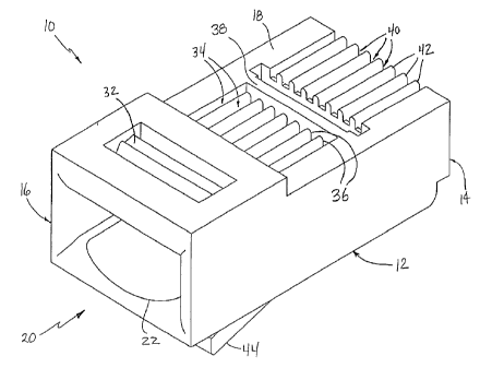
connector or plug indicated generally by reference numeral 1 0.
Plug 10 comprises a unipartite housing 12 which is specifically adapted to
terminate
a multi-conductor cable (not shown in FIGS. 1-4). Modular plug 10 in this
preferred
embodiment generally includes features which are generic to a standard modular
plug of the
type commonly used in both telephone equipment and other cable interconnect
applications.
6
CA 02291355 2000-03-10
A standard modular telephone plug having similar features is set forth, for
example, in U.S.
Patent Nos. 3,954,320 and 3,998,514, both of which are expressly incorporated
herein by
reference. Another version of a standard, miniature modular plug is set forth
in my earlier
U.S. Patent No. 4,412,715. However, as will be appreciated hereinafter, the
modular plug 10
of the present invention contains important structural and functional
modification! when
compared with the referenced prior art modular plugs.
Housing 12 of plug 10 includes a free end 14 which is adapted to be inserted
into a
mating modular jack such as the device described in U.S. Patent No. 3,850,497,
which is
expressly incorporated herein by reference. Such a jack typically includes a
plurality of side-
by-side spring contact members which are placed in a cavity adapted to receive
free end 14
of plug 10 for making electrical contact with certain of the plug's contact
terminals, as will be
described in greater detail below.
Housing 12 also includes a cord or cable input end 16 as well as a terminal-
receiving
side 18. The cable input end 16 includes a cord receiving cavity 20 into which
a multi-
conductor cable may be placed.
As shown in FIGS. 1-3, cord receiving cavity 20 includes a lower, cable-
receiving
trough 22 which comprises a semi-depression in the lowerwall of cavity 20
against which the
outer jacket of the cable rests.
As may be seen in FIG. 3, cord-receiving cavity 20 includes a relatively wide,
rear
cable-receiving portion 24, a middle conductor-receiving portion 26 located
forwardly of
portion 24, and a terminal-receiving portion 28 located at the forwardmost
portion of housing
12 near the free end 14 thereof. Positioned between conductor-receiving
portion 26 and
terminal-receiving portion 28 is a component-receiving portion 30.
Portions 26, 28 and 30 together define a substrate-receiving portion indicated
generally by reference numeral 62, which is provided for a purpose that will
be described in
greater detail hereinafter.
Referring now to FIGS. 1 and 4, in the top of housing 12, adjacent the cord-
receiving
cavity 20, is positioned a jacket anchoring member 32 which conventionally is
connected to
7
CA 02291355 2000-03-10
the housing by a hinge and includes a snap-lock ledge that forces member 32
against the
outer jacket of the cable to provide strain relief, all of which is quite
conventional.
Formed in the middle portion of housing 12 on the terminal-receiving side 18
is a first
set of terminal-receiving slots 34 which are defined by a first set of
terminal partitions 36.
Slots 34 are each sized so as to receive therein a standard, planar contact
terminal that will
be described below.
Positioned adjacent the first set of slots 34 is a transverse partition member
38. On
the other side of partition member 38 are positioned a second set of terminal-
receiving slots
40 which are, in turn, defined by a second set of terminal partitions 42
arranged side-by-side
in a manner similar to terminal partitions 36. Slots 40 likewise are each
sized so as to receive
a standard contact terminal, as will be described below. Further, the first
and second sets of
terminal receiving slots 34 and 40 are positioned on terminal receiving side
18 of housing 12
so as to be in substantial alignment with each other, as best seen in FIG. 4.
Referring back to FIG. 2, housing 12 also includes a standard locking tab or
latching
arm 44 which is pivotally mounted to the bottom wall of housing 12.
Alternatively, it may be
mounted to either side wall. As is conventional, latching arm 44 includes a
pair of spaced
shoulders 46 which are adapted to be secured by similarly spaced shoulder
retaining
members in the mating modular jack (not shown).
Referring nowto FIGS. 5 and 6, they correspond respectively to FIGS. 4 and 2,
except
that FIGS. 5 and 6 illustrate the plug 10 of the present invention with a
multi-conductor cable
50 installed therein. Multi-conductor cable 50 generally includes an outer
jacket that
surrounds a plurality of individually insulated conductors. Referring to FIG.
5, there are
illustrated a first set of contact terminals 48 positioned in the first set of
side-by-side terminal-
receiving slots 34. Similarly, a second set of contact terminals 52 are shown
positioned in
the second set of side-by-side terminal-receiving slots 40. FIG. 6 illustrates
the free end 14
of plug 10 as well as the second set of contact terminals 52 located in slots
40 which are
defined by the second set of terminal partitions 42.
FIG. 7 is a longitudinal sectional view of the structure illustrated in FIG. 5
wherein it
8
CA 02291355 2000-03-10
may be appreciated that multi-conductorcable 50 includes a plurality of
insulated conductors
54 that are terminated generally in the conductor-receiving portion 26 of the
connector. Also
illustrated in FIG. 7 is the pivotal mount 45 of the rearvvardly extending
latching arm 44.
FIG. 7 also illustrates the general structure of a preferred embodiment of the
first and
second set of contact terminals 48 and 52. Each of the contact terminals, such
as contact
terminal 52, includes conductor-piercing tangs 56 at the lower end thereof and
a spring-
contact mateable surface 58 at the other end thereof which is adapted to come
into contact
with the similarly-spaced spring contact portion of the mating modular jack,
as described
above. Contact terminals 48 and 52 are held in place respectively within slots
34 and 40 by
a press or interference fit within the reduced portions 55 and 65 of slots 34
and 40,
respectively.
Contact terminal 48 may be substantially identical in form to contact terminal
52. That
is, contact terminal 48 preferably includes a pair of conductor-piercing tangs
64 at the lower
end thereof and a spring-contact mate able surface 66 at the upper end
thereof. However,
surfaces 66 of contact terminals 48 are not intended in this embodiment to
mate with spring
contact portions of a mating jack, in contrast to the surfaces 58 of contact
terminals 52. More
particularly, contact terminals 48 are provided interalia to terminate the
insulated conductors
54 of cable 50, in a manner which will be described in greater detail
hereinafter.
In accordance with the present invention, a thin-flexible substrate indicated
generally
by reference numeral 60 is positioned within substrate-receiving portion 62 of
housing 12.
Substrate 60 is preferably positioned below conductors 54 which overlie
approximately 1 /3
to'h of the overall length of substrate 60, as seen clearly in FIG. 8.
Substrate 60 in this
embodiment is generally rectangular and formed of a thin (e.g., 0.0005 inch -
0.002 inch)
plastic, such as a polyester film, and is sized so as to be interference or
press fit along the
edges thereof with the side walls that form substrate-receiving portion 62.
The thickness of
substrate 60 will in part be selected according to the size of portion 62 and
the diameter of
insulated conductors 54. Substrate 60 is preferably flexible so as to be
easily manipulated
and well-fit within substrate receiving portion 62.
9
CA 02291355 2002-11-12
Referring now to FIG. 8, it is a view similar to FIG. 3 but shows the
substrate 60 of the
present invention together with a multi-conductor cable 50 both in position
within housing 12.
Formed on the upper surface of substrate 60 (or, alternatively, on the bottom
surface, or on
both surfaces thereof) by any conventional technique is a first set of metal
traces or
conductive paths 68. Details concerning the dimensions of the conductive
paths, the
thiclcnesses thereof, and the manner of formation of same are fully described
in my earlier
U.S. Patent No. 4,412,715 .
In this improvement over my earlier '715 patent, there are provided two
distinctly
separate sets of conductive paths: the first is designated by reference
numeral 68 which, as
1o noted above, are formed at one end of substrate 60 in alignment with the
position of insulated
conductors 54 which overlie same.
Positioned at the other end of substrate 60, and in alignment with the first
set of
conductive paths 68, is a second set of metal traces or conductive paths 72.
Again, traces
72 may be substantially identical in size to the aligned first set of traces
68. The second set
of traces 72 are also positioned so that each trace underlies a respective one
of the second
set of terminal-receiving slots 40, and hence contact terminals 52, as will be
described in
more detail below.
Located between the first and second set of traces 68 and 72 are a plurality
of
electrical or electronic components 70 which are selected and designed to act
in a specific
2o manner upon the electrical signals received from insulated conductors 54.
Each of the individual components 70 are electrically connected to adjacent
ends of
traces 68 and 72 to form an electrical series circuit. Of course, the
components 70 may be
the same or different components, and may or may not be provided in each of
the individual
positions on the substrate, as may be desired for a particular application.
Certain electrical
~mponents 70 may comprise, for example, simple resistors, while other
components may
comprise active devices, such as transistors or integrated circuits. Any
suitable electrical or
electronic component may be selected that acts in the desired predictable,
specific manner
CA 02291355 2000-03-10
upon an electrical signal that is desired to be modified.
It may be appreciated from FIGS. 7 and 8 that the first set of contact
terminals 48
terminate each of the individual insulated conductors 54 as well as the
underlying first set of
conductive paths 68 on substrate 60. Thus, the electrical signals appearing on
insulated
conductors 54 are electrically coupled, via contact terminals 48, to the first
set of metal traces
68.
It also may be appreciated from FIGS. 7 and 8 that the second set of contact
terminals
52 serve the function of piercing and thereby terminating the second set of
conductive paths
72 such that any signal appearing on paths 72 is transmitted through contact
terminals 52 to
the spring-contact terminals of the mating modular jack (not shown). Thus,
contact terminals
52 are used as terminating devices for substrate 60, but are not designed to
terminate the
insulated conductors 54.
In a similar vein, contact terminals 48 are used to terminate the insulated
conductors
54, but are not used to couple the signals therefrom to any external mating
modular jack.
Rather, contact terminals 48 couple the signal from conductors 54 to the
substrate 60.
Positioned between traces 68 and 72 are electrical components 70 which
respectively act on
the input signals from traces 68 so as to modify them in a predetermined
manner. The
modified signals are then fed to the output traces 72 so as to be coupled to
an output device
via contact terminals 52, as described above. In this manner, the incoming
signals on cable
50, appearing on individual insulated conductors 54, may be modified in a
precise,
predetermined manner by preselected electrical components 70 before being
output to a
mating modular jack.
Referring now to FIGS. 9 and 10, there is illustrated a second embodiment of
the
present invention. This second embodiment is quite similar to the first
embodiment shown
in FIGS. 7 and 8. However, in addition to the first set of electrical
components 70, there is
provided on substrate 60 a second set of electrical components 80 which are
preferably
series connected to the first set of components 70 by connecting traces or
conductive paths
75.
11
CA 02291355 2000-03-10
In this embodiment, the incoming electrical signals along insulated conductors
54 may
be modified both by the first set of electrical components 70 and the second
set of electrical
components 80 before being output to the mating modular jack (not shown). This
provides
an additional degree of design capability to the present invention.
Obviously, numerous modifications and variations of the present invention are
possible in light of the above teachings. For example, the electrical
components 70 and/or
80 may be vastly different, one from the other, depending on the desired
application. In
addition, the present invention may be used in other electrical connectors,
such as sub-
miniature D connectors and circular pin connectors. In viewthereof, it should
be understood
that within the scope of the appended claims, the invention may be practiced
otherwise than
as specifically described herein.
12