Note: Descriptions are shown in the official language in which they were submitted.
CA 02291380 1999-12-O1
CONNECTOR WITH PRESTRESSED CONTACTS AND ITS USE
BACKGROUND OF THE INVENTION
The present invention has for a subject a connector with prestressed contacts
and its use. Such a connector has elastic conductive strips provided with
contact
pins to be soldered, and an insulating stnucturc in which the elastic
conductive strips
are supported. The invention most particularly finds application in mounting
connectors on a printed circuit, notably in the surface mounting of connectors
designed to assure an electrical connection between microcircuits of a smart
card
and of electronic systems. These electronic systems are, in a preferred
example,
those of smart card readers or mobile telephones. This type of connector has
elastic
conductive strips designed to assure electrical contacts by pressure with
metallic
surfaces or contact areas present on the smart card. Moreover, the contact
between
the contact pins to be soldered of the connector and the surface of the
printed circuit
on which these pins must be soldered roust be a fiat contact. The invention
finds
interest due to the improvement of the coplaneity [inherent flatness) of the
electrical
contact between any contact pin to be soldered whatever and the surface of the
printed circuit.
Connectors designed for surface mounting that are currently manufactured
have contact pins to be soldered, one free end of which is chamtcred to form a
contact plane with the printed circuit Each contact pin to be soldered defines
a local
contact plane designed to come into contact with the printed circuit. Taking
into
account all the planes of local contact defines a distribution, in the
direction of the
thickness, of connector contacts with retard to the plane of the printed
circuit. In
Z~ fact, during the manufacture of a connector, the chamfering of the elastic
conductive
CA 02291380 1999-12-O1
strips is produced according to processes which do not easily permit obtaining
a
good repeatability with regard to the cvplaneity of the contact pins to be
soldered
(surface mounting). That is to say, appreciable differences of form andlor
dimensions may exist between two elastic conductive strips Qn the one hand,
one
contact pin of a strip to be soldered may not be perfectly planar. On the
other hand,
two contact pins to be soldered, each one of which stay be planar, may have
different contact planes andlor contact planes that are not parallel to one
another.
This type of connector thus presents problems.
In a s~eneral manner, this type of connector is comprised ofa thermoplastic
I O insulating structure and a certain number of bronze contacts, six in one
example.
'these contacts are treated and receive a triple coating of nickel, then tin-
lead, arid
finally a layer of gold for the part in contact with a smart card. The pins of
these
contacts are designed to be surface-mounted on a printed circuit. Now, in this
type
of design, during the use of the product, surface mounting of the connector,
as well
I5 as throughout the fife of the device on which it is mounted, sometimes
under
conditions of severe handling, the contact assembly of the connector must
adequately assure a sut~icient contact pressure for good electrical
transmission.
In fact, a smart card connector, for example, belonging to a mobile telephone
or any other electronic system likely to be subjected to vibrations, will
transmit these
ZO vibrations to the smart card as well as to the connector. In this case, a
lowering of
the contact pressure on the smart card is problematic, since, if a vibration
is too
strong, a Contact between the Smart card and the connector can be interrupted
or
defective, even for a brief instant, which can lead to reading or writing
errors of data
in the smart card.
CA 02291380 1999-12-O1
Thus, it was observed that in order for the contact with the smart card to be
judged satisfactory, it is necessary that the support plane of the connector's
contact
pins to be soldered are mersed or at least quasi-merged with the contact plane
of the
printed circuit. In fact, this coplanarity thus permits etlcctively conforming
to a
requirement called coplaneity [inherent flatness] necessary for implementing
the
process for surlaee mounting, CMS, a requirement which implies that any
cantaet
whatever must be found within a maximum tolerance range, which is desirably
small, retative to a support plane of the connector's contact pins to be
soldered on
the printed circuit, a support plane that defines a reference plane for said
coplaneity.
Moreover, the size constraints of the connector do not permit a sufficiently
precise guidance of the contact pins to be soldered. All this implies that
this support
plane evidently cannot be determined in a precise and reproducible manner and
therefore, a significant dispersion with regard to coplaneity is brought
about.
More precisely, in order to assure an effective CMS soldering, the outlets of
the components, i e., flue contact pins to be soldered must be designed to
permit
guaranteeing a coplaneity of less than 0.1 mm. This is translated in reality
by a
dimension X. representing a distance between the support face of the insulator
of the
component and the face to be soldered of the CMS outlets, whose tolerance
range is
0.1 mnt (X ~ 0.05 nun).
?0 This dimension X results from a double chamfering of an elastic conductive
strip (the contact zone with the smart card must be elastic) and it is the
elasticity of
this elastic conductive strip which is the cause of mast of the problems
encountered,
notably those defined previously. This elasticity varies as a function ofthe
material
used to create an elastic conductive strip, its thickness, or even the surface
treatment
2S applied. Thus, there are too many influences to assure obtaining, by mass
CA 02291380 1999-12-O1
production, elastic conductive strips with a tolerance of less than
approximately 0.05
millimeter.
Moreover, this problem leads to another problem. In fact, knowing that the
copianeity of the printed circuit with the contact plane has a high
probability of
being imperfect, each connector must be inspected. In addition to the number
of
rejections this entails, this piece-by-piece inspection is as lengthy as the
number of
connectors is large, which creates a loss of time and therefore an increase in
the
overall cost of such a connector
SUMMARY 4F THE INVENTION
The present invention has for a subject to remedy the problems cited by
proposing a connector havin5 an insulatin 5 structure and a multiple number of
elastic conductive strips, held in this structure, each strip being provided
with a
contact pin to be soldered. The insulating structure has fixed pieces aligned
in a
plane. The contact pins to be soldered are supposed on these fixed pieces in
this
plane by effect of a prestress applied to them. Thus, the contact surface of
the
contact pins to be soldered is found pressed into the plane ofthe fixed
pieces, with a
precision of the order of 0.02 mm, given that molding of insulators with such
precision is known. As a result, the contact between the connector's contact
pins to
ZO be soldered and the printed circuit surface is a perfectly flat contact
Thus, the
contact cones of the elastic strips with the smart card is also found in a
plane
perfectly parallel to the contact plane of the smart card.
The invention therefore concerns a connector laving an insulating structure
and a multiple number of elastic conductive strips, held in this insulating
structure,
?5 each elastic conductive strip being provided with a contact pin to be
soldered,
CA 02291380 1999-12-O1
characterized in that the contact pins to be soldered are prestres5ed and that
the
insulating structure has fixed pieces aligned in a plane on which the
prestrcsscd
contact pms press.
BRIEF DESCRIPTION OF THE DRAWINGS
The invention will be better understood upon reading the description that
follows and by examination of the figures that accompany it. The latter are
presented only by way of example arid are not at all limiting for the
invention. The
figures show:
- Figure I : a perspective view of the connector according to the invention;
- Figure 2: a perspective view of an elastic conductive strip of the connector
according to the invention;
- Figure 3: a plan view of an anchoring plate of the elastic conductive strip
with its two Lateral arms;
- Figure 4~ a sectional view of the connector according to the invention.
DETAILED DESCRIPTION OF TI-fE EMBODIM.ENI'S
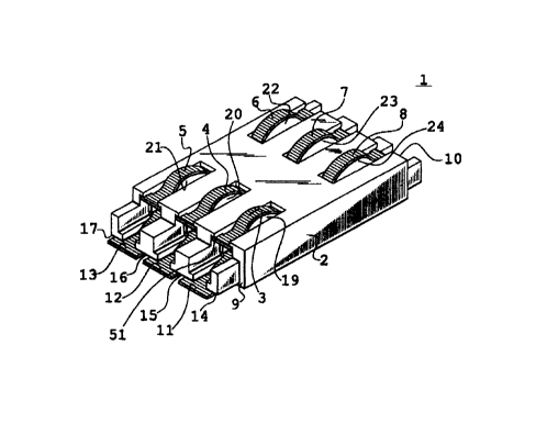
Figure 1 shows a connector 1 according to the invention. -This connector I '
has an insulating structure 2 and, in a preferred example, six elastic
conductive strips
3 to 8. They ace distributed by groups of three, symmetrically and regularly,
along
the two sides 9 and 10 of insulating structure 2, these two sides 9 and 10
being
opposed. 1n the following, we will limit the description to the elements
situated on
side 9, the elements of side 10 beins~ deduced tTOn l side 9 by symmetry.
The conductive elastic strips 3, 4, 5, respectively, are provided with contact
pins to be Soldered 11. 12, 13, respectively. In a preferred example, these
contact
,.
CA 02291380 1999-12-O1
pins to be soldered are in the form of flat plates and situated at the first
ends of strips
3, 4 and 5, respectively. In addition, these contact pins to be soldered I 1,
12 and I3
are arranged perpendicularly to side 9 of insulating structure 2 In addition,
insulating structure 2 has fixed pieces !4, iS, 16 and 1? regularly aligned in
a plane.
This plane is perpendicular to side 9. The contact pins t0 be soldered I i,
12, I3
have a generally "T"-shaped widening These T-shaped widenings, coming from
contact pins to be soldered ! l, 12, 13 are supported under tixed pieces !4,
15, l6
and I7. To do this, each contact pin to be soldered is situated between two
fixed
pieces. In a preferred example, fixed pieces 14 to I~ are stntcturcs rising
I0 perpendicularly to side 9 and have at least one flat face. 'these flat
faces are those
under which the contact pins to be soldered are supported These fixsd pieces
are
substantially rigid, so that the pressures applied by the contact pins to be
soldered
are insuff cient to deform the support planes of the fixed pieces. Thus, the
widcnings of the contact pin to be soldered I I are supported by two fixed
pieces 14
1 ~ and 15, the contact pin to be soldered 12 is supported by two fixed pieces
I 5 and 16
and so on The plane of fixed pieces 14 to 17 is by design (molding) obtained
within
the tolerance sought.
Figure 2 shows conductive elastic strip ~ outside connector 1 It has an
anchoring plate 18 placed in intermediate position. 'This intermediate
position is a
20 position in which anchoring plate 18 is closer to the end having the eomact
pin to be
soldered 11 than the other end of conductive elastic strip 3 This anchorinu~
plate l 8
is inserted forcefully into a housing 19 provided for this purpose in
insulating
structure 2 lnsulatins structure 2 also has housings fgr the other elastic
conductive
strips. In the example shown, insulating stnacture 2, therefore, has six
housings 19
25 to 24. This forceful insertion of anchoring plate l8 permits assuring a
fixed bond
CA 02291380 1999-12-O1
between anchoring plate ! 8 and insulating structure Z. This anchoring plate
18
projects laterally with two lateral arms 25 and 26. The forceful insertion of
anchoring plate t8 into housing 19 provided for this purpose in insulating
structure 2
has for an effect the inserting of the two lateral arms 25 and 26 into two
lateral
grooves made in each housing
Contact pin 1 I is prestressed so as to come to be pressed onto fixed pieces
14
and 15 once the strip is inserted.
This opposition of lixed pieces i4 and IS therefore maintains the
deformation of elastic conductive strip 3, which, while bein' permanent,
remains an
I O elastic deformation The prestress permits assuring the contact of the
contact pin tv
be soldered 11 on fixed pieces 14 and 15. In the connector of the invention,
it is
fixed pieces 14, l5, 16 and l 7 of side 9 of insulating structure ? that are
opposed to
the reaction forces applied by contact pins to be soldered I 1, ! 2 and I 3.
Insulating structure 2 is obtained, in a preferred example, by molding. The
molding processes used currently permit obtaining flat surfaces and dimensions
with
a precision ofthc orderof0 02 mrn (i.e., one can obtain surfaces whose relief
variations are contained in a space whose thickness can be reduced to
approximately
0 02 mm).
The elastic properties ofthe strip are thus used In fact, during support of
the
contact pins to be soldered on the fixed pieces, the reaction force is
sufficient to
obtain a deformation of the contact pins to be soldered, so that a contact
between a
contact pin to be soldered and a fxed piece is flat. Thus, the planeity
obtained in the
case ofthe invention for contact pins to be soldered I I, I2 and 13 i~ greater
than the
planeity obtained in the state of the art. "
_ CA 02291380 1999-12-O1
Figure 3 shows anchoring plate 18 provided with two lateral anus 25 and 26
The two attachment arms 25 and 26 are extended, in parallel to a plane passing
through anchoring plate 18, by two lateral attachment catches 27 and 28,
respectively. A lateral attachment catch 27 or 28 has a form of a harpoon or
wedge,
a first side 29 or 30 of which is perpendicular to an end 31 or 32 of one of
lateral
arms 25 or 2G, respectively. A second side 33 or 34 is oblique with regard to
end 3 I
or 32, respectively. Catches 27 and 28 are arranged such that, with regard to
the
direction of insertion of anchoring plate t 8, it is oblique sides 33 and 34
of catches
27 and 28 which first penetrate into grooves 35 and 36, respecaively, provided
for
this purpose in walls 37 and 38 of a housing 39. Sides 29 and 30 of catches 27
and
28 penetrate in second place.
At the beginning of insertion of lateral arms 25 and 26 into grooves 35 and
35, catches 27 and 28 penetrate into walls 40 and 4 i of grooves 35 and 36
respectively, facing one another. Thus the two catches 27 and 28 deform walls
40
I5 and 41 under the effect ofan insertion force applied to anchoring plate 18.
This
deformation of walls 40 and 4 t has for an efl''tct producing a compression
stress on
catches 27 and 28 and therefore attaching anchoring plate 18. At the end of
insertion, anchoring plate ! 8 comes to abut walls 42 and 43 constituting a
termination ofgrooves 35 and 3f, respectively. In this state, anchoring plate
l8
cannot advance further because of walls 42 and 43, nor can it laterally budge,
because of the compression stresses applied by walls 40 and 41, nor can it go
backwards, because of perpendicular sides 29 and 30 of catches 27 and 28 which
oppose any translation movement in this direction of anchorinJ plate 18.
Anchoring plate 18 is therefore fixed and daes~not possess any degree of
freedom. In addition, the two front corners 44 and 45 of anchoring plate 18
are
CA 02291380 1999-12-O1
chamfered. These two corners 44 and 45 are the anbles that are formed by ends
3 l
and 32 of lateral arms 25 arid 26 with sides 46 and 47, respectively. These
sides 46
and 47 are those which, at the end of insenion of anchoring plate t 8, enter
into
contact with walls 42 and 43 of grooves 35 and 3G, respectively. These
chamfered
corners 44 and 45 permit favoring the engagement of anchorage 18 in grooves 35
and 36, respectively.
Figure 4 shows a section of connector I along a sectional plane passing
through elastic conductive strips 3 and 8 (conductive elastic strip 8 is not
shown). In
a preferred example, a housing t9 receiving conductive strip 3 has a first
opening on
side 9 of insulating structure 2, as well as a second opening on a side 48
perpendicular to side 9 but parallel to the contact plane of the fixed pieces
Thus, elastic conductive strip 3, introduced in side 9 is compressed in
housing 19. For this, conductive elastic strip 3 has a folded-back form and
has a
second end 49, which is found in a parallel plane, and not merged, with the
plane
passing through anchoring plate J 8. A part of elastic conductive strip 3,
situated
between end 49 and anchoring plate 18, is chamfered in such a way that a piece
of
this part projects from the second opening of side 48, with a saddle-back
shape 50.
It is this portion ofcondurtive elastic strip 3 which is designed to produce
an
electrical contact between the smart card and connector t This contact zone of
saddle-back shape 50 with the smart card is mobile with regard to the
anchoring
plate.
Thus, this chamfered form of this part ofeiastic conductive strip 3 permits,
obtaining a spring eflcct ot~a portion oftitis part along an axis
perpendicular to side
48, when pressure is applied. This spring effect assures, in a preferred
example. an
electrical contact by pressure between elastic conductive strip 3 and a metal
contact
CA 02291380 1999-12-O1
..
area on the smart card. Moreover, end 49 of elastic conductive strip 3 is
subjected to
a second prestress. For this, it is held, by fixed pieces between walls 37 and
38 of
housing 19, at a height such that a deviation between a fixed piece 5 I, made
in wall
38, and the plant passing through anchoring plate 18 is less than the
deviation
S between this same plane and end 49, when it is not subjected to any stress
End 49
can therefore only move in a housing 32 in a single direction, which is
opposite
fixed piece 51. A T-shaped wideninly of end 49 of elastic conductive strip 3
permits
taking support on this fixed piece 5 I The latter prestress has ter an
objective
notably to assure approximately the same contact plane for all the contact
zones, this
t0 contact plane being parallel to the contact plane of the contact pins to be
soldered.
The deviation between a peak 53 of the saddle-back and side 48 is such that a
forcing of saddle-back 50 into housing I9, resulting from pressure applied by
the
smart card during the connection, always leaves at least end 53 outside of
housing
19. Thus the resulting rcactian force assures a sufficient pressing together
of the
15 contact zones of connector t un the contact areas of the smart card so as
to have an
electrical contact by pressure according to the criteria disclosed above.
During the insertion of an elastic conductive strip 3 in housing 19 of
insulating structure 2, it is necessary to resiliently bend end 49 towards
anchoring
plate t8. This pcrrnits end 49 to be inserted into housing 52. After release
of the
?0 bending force, end 49 comes to abut fixed piece 51. Moreover, during
insertion,
contact pin l 1 of elastic conductive strip 3 is placed as defined previously.
In this
case, elastic conductive strip 3 is subjected to two reaction prestresses with
anchoring plate I 8. The first prestress is that of contact pins to be
soldered t 1, t 2
and 13 on fixed pieces 14, I5, 16 and 17. In the example, two fixed pieces are
used
?: to create a prestress on one contact pin to be soldered Thus each contact
pin to be
CA 02291380 1999-12-O1
soldered is found between two fixed pieces. A consequence of this placement of
the
contact pins to be soldered between the fixed pieces is that the strips arc no
longer
mobile. Thus the risks of catching an attachment strip during the mounting
operations is limited.
S Insulating structure 2 is made, in a preferred example, by molding an
insulating thermoplastic material. Such materials have properties of
elasticity and
deformation used notably Burins insertion of the anchorin's for the conductive
elastic strips as explained above. Elastic conductive strips 3 to 8 arc
bronze, in a
preferred example, bronze being an elastic and easy-to-shape material. That is
to
I O say, it can be deformed easily. This is one of the objectives sought when
the contact
strips come to be supported on the fixed pieces of the insulating structure.
The
contact strips thus mate with the relief shape formed by the faxed pieces.
Moreover,
the saddle-back structure of the elastic conductive strip, assuring contact
with a
smart Card, is coated with nickel, a tin-lead alloy and/or gold, in order to
improve the
15 contact characteristics of the elastic conductive strip and thus to favor a
good
electrical contact between connector l and a smart card.
It is also to be noted teat, in general, the contact pins of CMS outlets are
easily deformable and that, consequently, the tixed piece permits also
assuring
protection of said pins during any manipulation.