Note: Descriptions are shown in the official language in which they were submitted.
CA 02291610 1999-11-29
WO 98/54854 PCT/US98/09932
1V~ODULATION FORMAT an m TINC n~ICAI, TRANSPONDERS
FIELD OF THE INVENTION-
The invention relates to optical transponders generally and, more
particularly, to
optical transponders which change the modulation format of incident optical
signals.
BACKGROUND OF THE INVENTION~
Optical communication systems are a substantial constituent of communication
networks. The expression "optical communication system," as used herein,
relates to any
system which uses optical signals to convey information across an optical
waveguiding
medium. Such optical systems include, but are not limited to,
telecommunications systems,
cable television systems, and local area networks (LANs). Optical systems are
described in
Gowar, Ed. Optical Communication S stems (Prentice Hall, NY) c. 1993, the
disclosure of
which is incorporated herein by reference.
1 S Optical transmitters are typically available in a particular modulation
format.
Depending upon the transmission medium for a given optical system, it may be
desirable to
use a specific modulation format to enhance the transmission characteristics
of the launched
optical signal.
In some optical systems wavelength division multiplexing (WDM) is employed to
increase the capacity of the fiber optic network. In a WDM system, plural
optical channels
are carried over a single waveguide, each channel being assigned a particular
wavelength.
To provide compatibility of the WDM format with existing networks, it is
desirable to
convert a signal from a received transmission wavelength to a specific channel
wavelength
within the WDM system. In assignee's prior patent and patent application, U.S.
5,504,609
and serial number 08/624,269, the disclosures of which are incorporated herein
by
CA 02291610 1999-11-29
WO 98/54854 PCT/US98/09932
reference, a series of optical remodulators are used to take input signals
from various optical
transmitters and output the information onto optical channels within the
channel plan of a
WDM optical system. Typically, the modulation formats of the optical signals
output by
the optical transmitters and the remodulators is the same. However, depending
upon the
type of optical receivers employed and the transmission characteristics of the
optical system,
it may be desirable to change the modulation format of the optical
transmitters to a format
which is better suited to transmission in the WDM optical system.
Thus, there is a need in the art for optical transponders which can change the
modulation format of incident optical signals. There is a further need in the
art for
improved WDM optical communication systems which can receive incoming optical
transmitter signals of various modulation formats and place the information
onto WDM
system optical channels in a different modulation format from that of the
transmitter optical
signals.
1 S SUMMARY OF THE INVENTION
The present invention provides a modulation format adjusting optical
transponder
for receiving an incident optical signal of a first modulation format and
outputting an optical
signal having a different modulation format. The transponder includes an
optical-to-
electrical conversion element configured to receive an information-bearing
optical signal
having a first modulation format and output an electrical signal corresponding
to
information from the incident optical signal. The transponder includes a laser
for outputting
an optical carrier signal at a selected wavelength and a modulator
communicating with the
optical-to-electrical conversion element and with the laser. The modulator
places the
-2-
CA 02291610 1999-11-29
WO 98/54854 PCT/US98/09932
information from the incident optical signal onto the optical signal output by
the laser,
creating a modulated optical output signal having a second modulation format
different
from the first modulation format. Advantageously, the optical transponders of
the present
invention can take optical signals in a common modulation format, such as
amplitude
modulation, and output optical signals in a power-flat modulation format, such
as frequency
shift key (FSK) modulation. The modulation format adjusting optical
transponders of the
present invention can be used as remodulators for wavelength division
multiplexed optical
systems.
BRIEF DESCRIPTION OF THE DRAWINGS
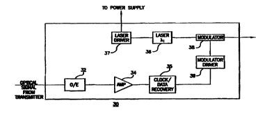
FIG. 1 schematically depicts a modulation format adjusting optical transponder
according to the present invention.
FIG. 2 schematically depicts a wavelength division multiplexed optical
communication system employing the optical transponder of FIG. I as an optical
I S remodulator.
DETAILED DESCRIPTION:
Turning to the drawings in detail, FIG. 1 schematically depicts a modulation
format
adjusting optical transponder 30 according to the present invention.
Transponder 30
receives an optical signal output by an optical transmitter. The input optical
signal is
converted by optoelectronic converter 32, typically a photodiode, to an
electrical signal.
The resultant electrical signal is amplified by amplifier 34, and routed
through clock and
data recovery circuit 35. Following retiming, the electrical signal passes to
modulator
-3-
CA 02291610 1999-11-29
WO 98/54854 PCT/US98109932
driver 39 which drives modulator 38. (It is noted that while modulator 38 is
an external
modulator such as a Mach-Zehnder modulator, other techniques for modulating
the optical
signal including electroabsorption modulators and direct modulation can be
used in the
present invention.)
Transponder 30 includes an optical source, such as laser 36, for delivering a
non-
information-bearing optical Garner signal to the laser output waveguide. In an
exemplary
embodiment, laser 36 is a DFB semiconductor diode laser, generally comprising
one or
more III-V semiconductor materials, commercially available from a wide variety
of
suppliers such as Fujitsu, GEC Marconi, and Hewlett-Packard. The laser outputs
an optical
carrier signal at a particular optical wavelength, ~,, (which, in the case of
a WDM optical
system, is a wavelength corresponding to a demultiplexer wavelength included
in a
receiving system). Laser driver 37 provides the required laser bias current
through a
suitable power supply (not shown) as well as thermal control of the laser
wavelength.
An optical wave in a single mode fiber of a certain center frequency has three
parameters which can continuously vary with time: amplitude, phase
(frequency), and state
of polarization. What is meant by "modulation format" is that one of these
attributes, or a
coupled combination of these, is made to vary in accordance with the
information being
imparted to that optical wave. The other parameters are not constrained to
follow the
information signal. Two modulation formats are different if the coupled
confirmation of
optical wave parameters (which can refer to a single parameter being varied)
are
substantially different. Modulator 38 uses a modulation format different from
the
modulation format of the optical signal input to optoelectronic converter 32.
As used
herein, the expression "modulation format" refers to the variation of one or
more optical
-4-
CA 02291610 1999-11-29
WO 98/54854 PCT/US98/09932
parameters such as amplitude, phase (frequency), and state of polarization to
impart
information to a carrier optical signal. Typically, the incident optical
signals are amplitude
modulated. Advantageously, transponders 30 can employ modulators with power
flat
modulation formats such as frequency shift key (FSK) or polarization shift key
(PoISK) to
create optical signals which do not create time-dependent power variations
within the
optical system. A particularly preferred modulation format creates a non-zero
chirped
optical signal, a modulation format which varies both the amplitude and phase
of the optical
signal. Using the modulation format adjusting optical transponders, incident
amplitude-
modulated optical signals from optical transmitters can be converted to
optical signals with
a power-flat modulation format. However, it is understood that the invention
encompasses
any transponder which uses a modulator having a modulation format, whether
amplitude,
frequency, phase, or polarization based (or a combination thereof), which is
different from
the modulation format of the incident optical signal. Various modulation
formats are
described in further detail in the Gowar reference, cited above, and in
Schwartz,
Information. Transmission Modulation and Noise (McGraw-Hill, New York), c.
1990, the
disclosure of which is incorporated by reference herein.
FIG. 2 depicts a wavelength division multiplexed optical communication system
10
employing the modulation format adjusting transponders of FIG. 1 as optical
remodulators.
Optical communication system 10 takes optical transmission signals from
diverse optical
transmitters and other optical signal sources and maps the signal sources onto
a wavelength
division optical communication system, i.e., a communication system in which
individual
optical signals correspond to optical channels within a wavelength division
multiplexed
optical signal carried on an optical waveguide.
-5-
CA 02291610 1999-11-29
~WO 98/54854 PCT/C1S98/09932
In the exemplary embodiment of FIG. 2, optical transmitters 20 are used to
provide
the information that will be carried by the optical channels within the WDM
optical system.
Optical transmitters 20 generally includes a laser, such as a DFB
semiconductor laser, and a
modulator for creation of an information-bearing optical signal. The
expression
"information -bearing optical signal," as used herein, refers to an optical
signal which has
been coded with information, including, but not limited to, audio signals,
video signals, and
computer data, generally through modulation. Alternatively, particularly for
short-reach
optical transmitters, the laser of optical transmitter 10 can be directly
modulated. Because
some of the transmitters may form part of an existing optical system, a wide
variety of
transmitters emitting in a broad range of wavelengths can be accommodated in
the optical
communication system of the present invention, thus ensuring compatibility
with currently-
deployed transmission equipment. Typical transmitters emit wavelengths ranging
from
about 1300 to 1600 nm. Transmitters in current optical communication systems
and various
optical modulation techniques employed therein are described in Gowar, O tical
Communication S, std, incorporated by reference above. Optical transmitters
suitable for
use in the present invention are commercially available from NEC, Fujitsu,
Alcatel, and
Nortel.
Optical communication system 10 uses the modulation format adjusting
transponders 30 of FIG. 1 as remodulators 130 for receiving the transmitted
infonnation-
bearing optical signal and outputting an information-bearing optical signal at
a WDM
optical system channel wavelength ~,~. The subscript j ranges from 1 to 16 for
the exemplary
optical system of FIG. 1 but can also be, for example, 4, 8, or 32 depending
upon the
capacity needs of the optical route services by the system. Typically, the
wavelengths
-6-
CA 02291610 1999-11-29
WO 98/54854 PCT/US98/09932
emitted by the remodulators are selected to be within the 1 S00 nanometer
range, the range
in which the minimum signal attenuation occurs for silica-based fibers. More
particularly,
the wavelengths emitted by the remodulators are selected to be in the range
from 1530 to
1 S60 nanometers. However, other wavelength bands may be selected according to
overall
S system requirements.
Each optical channel is routed to optical combiner SO for conveyance to
optical
waveguide 60. Optical combiner SO is selected from any passive optical
component which
can combine plural wavelengths into a single output medium. Frequently,
optical splitters
used to divide a signal among plural outputs are used as optical combiners,
operated in
reverse fashion from the splitter. Exemplary optical combiners include 1 x N
passive
splitters available from Corning, Inc., Corning, NY, 1 x N wideband single
mode splitters
available from IOT Integrierte Optilc GmbH, Waghausel-Kirrlach, Germany, and
fused fiber
combiners available from Gould, Inc., Millersville, MD. The combination of
channels
forms a multiplexed optical signal which is output to waveguide 60. Optical
waveguide 60
1 S is typically a single-mode optical fiber such as SMF-28, available from
Corning, and
TRLTEWAVE, available from AT&T Corp./Lucent Technologies, and is the principal
transmission medium for the optical communication system. However, any optical
waveguide which is capable of transporting multiple optical wavelengths can be
employed
as waveguide 60 in optical system 10.
Optionally interposed along optical waveguide 60 are one or more optical
amplifiers
70. Optical amplifiers 70 are selected from any device which directly
increases the strength
of plural optical signals without the need for optical-to-electrical
conversion. In general,
optical amplifiers 70 are selected from optical waveguides doped with rare
earth ions such
_7_
CA 02291610 1999-11-29
VVO 98/54854 PCT/US98/09932
as erbium, neodymium, praseodymium, ytterbium, or mixtures thereof. Optical
amplifiers,
their materials , and their operation are further described in Gowar, Ed.
tical
Communication S,~stems, incorporated by reference above and in Desurvire,
Erbium-Doled
Fiber Amplifiers, (John Wiley & Sons, Inc., NY), c. 1994, and Bjarklev,
Optical Fiber
Amplifiers: Design and S,vstem Applications. (Artech House, Norwood, MA) c.
1993 the
disclosures of which are incorporated by reference herein. An exemplary
optical amplifier
configuration is disclosed in U.S. Patent application serial number
08/554,976, the
disclosure of which is incorporated by reference herein. Alternatively, other
optical
amplifiers, such as semiconductor optical amplifiers, may be used along
transmission line
60.
Following transmission and amplification of the multiplexed optical signals
along
waveguide 60, each channel must be demultiplexed and routed to the receiver
designated for
the particular ~,~ channel. The multiplexed signal is input to optical
splitter 80 which places
a portion of the multiplexed signal onto plural output paths 82. Each output
path 82
optically communicates with a receiving system 90. Optical splitter 80 is
selected from any
optical device which can divide an input optical signal and place it onto
plural output paths.
Exemplary splitters include passive optical components such as those
components described
for use as optical combiner 50. Receiving systems 90 typically include
wavelength
selectors (not shown) for selecting the particular channel, ~,~ from the
multiplexed signal and
a receiver (not shown). Exemplary receiving systems are described in U.S.
Patent No.
5,504,609 incorporated by reference above.
While the foregoing invention has been described in terms of the embodiments
discussed above, numerous variations are possible. Accordingly, modifications
and changes
_g_
CA 02291610 1999-11-29
WO 98/54854 PCT/ITS98/09932
such as those suggested above, but not limited thereto, are considered to be
within the scope
of following claims.
-9-