Language selection

Search

Patent 2291724 Summary

Third-party information liability

Some of the information on this Web page has been provided by external sources. The Government of Canada is not responsible for the accuracy, reliability or currency of the information supplied by external sources. Users wishing to rely upon this information should consult directly with the source of the information. Content provided by external sources is not subject to official languages, privacy and accessibility requirements.

Claims and Abstract availability

Any discrepancies in the text and image of the Claims and Abstract are due to differing posting times. Text of the Claims and Abstract are posted:

  • At the time the application is open to public inspection;
  • At the time of issue of the patent (grant).
(12) Patent Application: (11) CA 2291724
(54) English Title: PRECISION OPTICAL FIBER ARRAY CONNECTOR AND METHOD
(54) French Title: CONNECTEUR DE GROUPEMENT DE FIBRES OPTIQUES DE PRECISION ET PROCEDE
Status: Dead
Bibliographic Data
(51) International Patent Classification (IPC):
  • G02B 6/36 (2006.01)
  • G02B 6/38 (2006.01)
  • G02B 6/42 (2006.01)
(72) Inventors :
  • SHERMAN, JONATHAN (United States of America)
  • CAMLIBEL, IRFAN (United States of America)
  • RICH, ERNEST J. (United States of America)
  • RICH, THEODORE, C. (United States of America)
(73) Owners :
  • FIBERGUIDE INDUSTRIES, INC. (United States of America)
(71) Applicants :
  • FIBERGUIDE INDUSTRIES, INC. (United States of America)
(74) Agent: NORTON ROSE FULBRIGHT CANADA LLP/S.E.N.C.R.L., S.R.L.
(74) Associate agent:
(45) Issued:
(86) PCT Filing Date: 1998-06-05
(87) Open to Public Inspection: 1999-01-07
Availability of licence: N/A
(25) Language of filing: English

Patent Cooperation Treaty (PCT): Yes
(86) PCT Filing Number: PCT/US1998/011851
(87) International Publication Number: WO1999/000687
(85) National Entry: 1999-11-26

(30) Application Priority Data:
Application No. Country/Territory Date
08/883,066 United States of America 1997-06-26

Abstracts

English Abstract


An optical fiber array connector in which the tolerance of the diameter of the
mask openings are not factors in the overall positioning of the plurality of
fibers (10). The array includes a mask element with rear and forward surfaces
(26, 24) and a plurality of openings that communicate through these surfaces.
A plurality of optical fibers include fiber ends having subtantially truncated
conical side surfaces that extend through the openings and engage the portions
of the mask openings nearest the mask rear surface (26). A method includes
preparing the fibers (10) to form a conical surface at their distil ends (14),
preparing the openings in the primary mask each with a diameter less than the
diameter of the fiber cladding or second layer, inserting the conical fiber
ends until the conical surfaces engage the mask opening walls (22), applying
bonding material to the mask forward surface (24) and exposed tips, grinding
and polishing the exposed tips and bonding material surface to truncate the
cones and expose the fiber core diameters.


French Abstract

L'invention concerne un connecteur de groupement de fibres optiques dans lequel la tolérance du diamètre des ouvertures du masque n'est pas un facteur entrant en ligne de compte pour le positionnement global des différentes fibres (10). Le groupement comprend un masque à surfaces arrière et avant (26, 24), avec plusieurs ouvertures communiquant à travers ces surfaces. Plusieurs fibres optiques ont des extrémités à surfaces latérales sensiblement tronconiques qui s'étendent à travers les ouvertures et viennent dans les parties de ces ouvertures de masque situées le plus près de la surface arrière (26) du masque. L'invention concerne aussi un procédé pour la préparation des fibres (10), qui consiste à former une surface conique à leur extrémité distale (14), à préparer les ouvertures dans le masque primaire chacune avec un diamètre d'ouverture inférieur au diamètre de la gaine ou de la seconde couche des fibres, à insérer les extrémités coniques des fibres jusqu'à ce que les surfaces coniques des fibres viennent dans les parois (22) des ouvertures du masque, à appliquer un matériau liant à la surface avant (24) du masque et aux extrémités à nu, à meuler et à polir les extrémités à nu et la surface du matériau liant pour obtenir les formes tronconiques, et à exposer le diamètre des âmes des fibres.

Claims

Note: Claims are shown in the official language in which they were submitted.


WE CLAIM:

Claim 1. An optical fiber array connector comprising a primary mask element
having
a rear surface and a forward surface and a plurality of mask walls defining
mask openings that
communicate through said rear and forward surfaces,
at least two optical fibers each comprising a core, a second fiber layer
extending over
said core and a jacket extending over a portion of said second layer,
each said optical fibers having one end in which said second layer and core
extend
beyond the jacket and in which the distal portion of said second layer has a
substantially
truncated conical side surface, said substantially truncated conical side
surface extending
entirely through the respective one of said wall openings and engaging a
portion of said
respective mask wall located substantially contiguous to said rear surface.

Claim 2. A connector according to Claim 1, wherein the smallest dimension of
said
truncated conical side surface is equal to or greater than the diameter of
said core.

Claim 3. A connector according to Claim 2, wherein the extreme ends of said
core
and truncated conical side surface extends forward of the forward mask
surface, and said
extreme ends are polished to a plane that is generally parallel to said
forward mask surface.


11


Claim 4. A connector according to Claim 1, wherein said truncated conical side
surface has at least a forward portion spaced from said respective mask wall,
and bonding
material located in said space for bonding together said truncated conical
side surface and
said respective mask wall.

Claim 5. A connector according to Claim 4, wherein said bonding material is
located on said forward mask surface and has a forward surface that has been
ground.

Claim 6. A connector according to Claim 1 further comprising a fiber guide
mask
having a rear guide surface and a forward guide surface, and having guide
openings for
guiding a respective plurality of fiber ends through the respective rear
portions of said
mask openings.

Claim 7. A connector according to Claim 6, wherein said forward guide surface
contacts said rear surface.

Claim 8. A connector according to Claim 6, wherein said forward guide surface
is
spaced from said rear surface.

12


Claim 9. A method of making an optical fiber array comprising:
preparing at least two optical fibers by cutting them to desired lengths,
forming the
core and second layers of one tip of each fiber into a conical shape,
preparing a mask wafer by forming a plurality of spaced fiber openings
communicating between the rear and forward surfaces of the wafer, at least two
of said
openings each having a wall portion contiguous to said rear surface with a
transverse
direction less than the largest diameter of said fiber second layers,
inserting the tip of each fiber into a respective openings so that the conical
side wall
of the tip engages the mask opening wall at said wall portion to stop the
forward insertion
of the fiber tip and the forward end of the tip extends beyond the forward
surface of the
mask, and securing the two fibers to the mask wafer.

Claim 10. A method of making an optical fiber array according to claim 9
further
including after said securing step removing the extreme end of the tip until
at least the
substantially full diameter of the core of each of the two fibers is exposed.

Claim 11. A method of making an optical fiber array comprising:
preparing at least two optical fibers by cutting them to desired lengths,
forming the
core and second layers of one tip of each fiber into a conical shape,
preparing a mask wafer by forming a plurality of spaced fiber openings
communicating between the rear and forward surfaces of the wafer, at least two
of said

13


openings having a transverse direction less than the largest diameter of said
fiber second
layers,
inserting the tip of each fiber into a respective openings so that the conical
side wall
of the tip engages the mask opening wall and the forward end of the tip
extends beyond the
forward surface of the mask, and securing the two fibers to the mask wafer,
removing the extreme end of the tip until at least the substantially full
diameter of the
core of each of the two fibers is exposed, and wherein
said removal step includes one of grinding and polishing the tip of the cones
in a
direction generally parallel to the forward surface of the mask wafer.

Claim 12. A method of making an optical fiber array according to claim 9
wherein
securing comprises applying bonding material to the forward surface of said
mask wafer and
the tips of the two fibers extend beyond the forward surface.

Claim 13. A method of making an optical fiber array according to claim 12
wherein
securing further comprises applying bonding material between the walls of the
mask openings
and the fiber tips positioned therein.

Claim 14. A method of making an optical fiber array comprising:
preparing at least two optical fibers by cutting them to desired lengths,
forming the
core and second layers of one tip of each fiber into a conical shape,


14


preparing a mask wafer by forming a plurality of spaced fiber openings
communicating between the rear and forward surfaces of the wafer, at least two
of said
openings having a transverse direction less than the largest diameter of said
fiber second
layers,
inserting the tip of each fiber into a respective openings so that the conical
side wall
of the tip engages the mask opening wall and the forward end of the tip
extends beyond the
forward surface of the mask, and securing the two fibers to the mask wafer,
securing comprises applying bonding material to the forward surface of said
mask
wafer and the tips of the two fibers extend beyond the forward surface, and
wherein
said removal includes grinding a portion of the forward surface portion of the
bonding
material.
Claim 15. A method of making an optical fiber array according to claim 9
wherein
said inserting includes guiding said fibers into the respective openings with
the use of a guide
mask.
Claim 16. A method of making an optical fiber array according to claim 15
wherein
said guide mask has a plurality of guide openings each aligned with a
corresponding mask
opening and each guide opening having a diameter greater than the greatest
diameter of said
conical side wall.


15


Claim 17. A method of making an optical fiber array according to claim 16
wherein
said guide mask contacts said mask.
Claim 18. A method of making an optical fiber array according to claim 16
wherein
said guide mask is spaced from said mask.
Claim 19. An optical fiber array made by the method of claim 9.
Claim 20. An optical fiber array connector comprising a primary mask element
having a rear surface and a forward surface and at least two mask walls
defining at least two
mask openings that communicate through said rear and forward surfaces,
at least two optical fibers and a jacket extending over a portion of each of
said fibers,
each said optical fibers having one end extending beyond the jacket and in
which the
distal portion of said end has a substantially truncated conical side surface,
said substantially
truncated conical side surface extending entirely through one of said mask
openings and
engaging a portion of the respective mask wall located substantially
contiguous to said rear
surface.
Claim 21. An optical fiber array made by the method of Claim 11.
Claim 22. An optical fiber array made by the method of Claim 14.


15/1

Description

Note: Descriptions are shown in the official language in which they were submitted.


CA 02291724 1999-11-26
- WO 99/00687 - PGT/US98/11851
PRECISION OPTICAL FIBER ARRAY CONNECTOR AND MEI~iOD
BACKGROUND:
The present invention relates to fiber optic arrays and more particularly to
high
precision fiber optic arrays and methods of making the same.
Fiberoptics has been the driving force in the communication revolution which
has
enabled carriers to achieve enormous data throughput. In order to realize the
firll potential
of the technology, fiberoptics will be incorporated into every facet of the
integrated
electronics, which will then make it possible to fully utilize the enormous
bandwidth of the
optical fiber with the high speeds of the semiconductor integrated circuitry.
To this end, arrays of optical fibers need to be coupled precisely and
reliably to
semiconductor laser and detector arrays on a chip. Already, various groups
throughout
the world have demonstrated feasibility of high speed optoelectronic VLSI
switching and
two dimensional fiberoptic arrays for an optical crossbar switch. See, for
example, High-
1


CA 02291724 1999-11-26
WO 99/00687 - PCT/US98/11851
Speed Optoelectronic VLSI Switching Chip with >4000 Optical I/O Based on Flip-
Chip
Bonding of MQW Modulators and Detectors to Silicon CMOS, Anthony L. Lentine,
et
al., IEEE Journal of Selected Topics in Quantum Electronics, Vol. 2, No. 1,
pp. 77, April
1996, and Fabrication of Two-Dimensional Fiber Optic Arrays for an Optical
Crossbar
Switch, GeoffM. Proudley, Henry White, Optical Engineering, February 1994,
Vol. 33
No.2., pp. 627-635., incorporated herein by reference.
The above publications purport to achieve a fiber array positionaI accuracy of
approximately +/- 5 micrometers. However, the fact that the precision
achievable with
optoelectronic devices such as charge couple devices (CCD's), photodetector
and laser
using semiconductor technology is almost an order of magnitude (0.5
micrometers) or
better indicates a strong need for new switching array designs and
manufacturing
techniques to attain much better fiber array precision so that these
technologies function
together.
Fiberguide Industries has already produced 10 x 10 arrays with positional
accuracies (center-to-center spacing error) of better than +/-5 micrometers.
The process
used takes advantage of the positional accuracy provided by the excimer laser
machined
0.010" thick polyimide wafers used in the assembly of the arrays.
Notwithstanding the above mentioned process, a need exists for high precision
fiber arrays with center-to-center spacing errors not exceeding ~2
micrometers.
2


CA 02291724 1999-11-26
WO 99/00687 - PCTNS98/11851
SUMMARY OF EXEMPLARY EMBODIMENTS
A high precision fiber array according to the principles of the present
invention
achieves the fiber center spacing not to exceed t2 micrometers specification
with current
excimer laser technology and perhaps better results with future laser
technology. This
high precision is obtainable for single mode and multimode fibers.
This new precision is obtainable according to an embodiment of the present
invention by imparting a hole diameter in the mask that is less than the
minimum diameter
of each respective fiber. The fiber ends are processed into a cone-shaped tip
which is
inserted into respective holes until the cone surfaces make good contact with
the walls of
the openings with potentially various tip lengths protruding from the opposite
side of the
mask. Each cone is shaped such that the fiber cone extends through the mask
opening
sufficiently to enable the full core cross section to be exposed after the
fiber ends have
been ground and polished, for example, as described below. This unique
arrangement and
method eliminates the hole diameter variation of t2 micrometer as an element
or problem
that contributes to imprecise fiber spacing. The exposed tips and holes then
receive epoxy
or other suitable bonding material to firmly secure the tips and mask. The
completed
assembly is then ground and polished and tested in the usual manner.
In one preferred embodiment, a guide mask cooperating with the above mentioned
primary mask serves to guide the fiber ends into alignment with the opening in
the primary
mask during assembly.
Also, the mask/fiber holder can be part of the final connector for ease of
assembly.
3

CA 02291724 1999-11-26
- WO 99/00687 - PCTNS98/11851
DRAWINGS
Other and further advantages and bene5ts will become apparent with the
following
detailed description of exemplary embodiments when taken in view of the
appended
drawings, in which:
Figure 1 is a list of salient steps to one example of the method according to
the
principles of the present invention.
Figure 2 is a partial section view of a fiber end prepared according to the
method
of Figure 1.
Figure 3 is a partial section of a primary fiber mask or wafer according to
the
present invention.
Figure 4 is a partial section of the fiber tip of Figure 2 inserted into the
primary
mask opening of Figure 3.
Figure 5 is the same as Figure 4 after bonding material is applied.
Figure 6 is the same as Figure 5 after the forward surface has been ground and
polished.
Figure 7 is the same as Figure 5 showing an alternate embodiment according to
the
present invention.
Figure 8 is the same as Figure 5 showing yet another alternate embodiment
according to the present invention.
4


CA 02291724 1999-11-26
WO 99/00687 - PCT/US98/11851
Figure 9 is a partial perspective of the fiber holder and fiber-wafer sub-
assembly
according to the present invention.
Figure 10 is an exploded view of a connector according to the present
invention
including the parts shown in Figure 9 and the semiconductor chip holder.
DETAILED DESCRIPTION OF PREFERRED EMBODIIVVIENT
With reference to Figures 1 to 4, a method according to the principles of the
present invention includes preparation of the optical fibers 10 by cutting a
number of fibers
to desired length. Each fiber includes a central core 11, a second or cladding
layer 13 and
a protective buffer, coating, or jacket 12. One end of each fiber is processed
so that the
outer jacket 12 (eg plastic, acrylic, NYLON, etc.) is stripped to expose a
predetermined
length T. A standard hot sulfuric acid strip technique can be used to strip
most jackets.
Thereafter, the exposed fiber tip is shaped to form a conical tip 14. In one
example, the
hare fiber tip with a fiber diameter (FD) is dipped into hydroflouric acid for
about 10
minutes then rinsed and dried.
The primary mask 20 according to the principles of the present invention can
be
made of any suitable material including polyimide, ceramic or metal. Fiber
openings are
preferably laser cut from the rear (fiber insertion) side in any suitable
predetermined
pattern with predetermined spacing. One exemplary pattern is shown in Figure
9, ie. a


CA 02291724 1999-11-26
WO 99/00687 PCT/US98/11851
1 o x 1 o array.
As better seen in Figure 4, because each primary mask opening is laser cut,
the
wall 22 forming the opening is slightly flared outward from the central
opening axis in the
direction of the forward surface. Accordingly, the primary mask opening
diameter
(PMD), which can be precisely placed within ~l to X1.3 microns in the X, Y
plane, can be
made accurately to within f2 microns at the rear surface 26. As seen below,
the precision
accuracy of the PMD, the nature of the flaring walls 22, and the diameter of
each opening
at the forward surface 24 of primary mask 20 are all insignificant according
to the present
invention. This results from the requirement that PMD must be selected to be
less than
the fiber diameter FD. Also, PMD should be great enough to enable enough of
the fiber
tip 14 to exit the forward mask surface 24 so that the full core diameter is
exposed after
polishing described below.
To assemble the array, each prepared fiber 10 is inserted into respective mask
openings from the rear surface until the tip conical surface 14 engages the
wall 22 of the
opening. See Figure 4. This engagement stops the forward insertion of the
fiber.
It will be understood that various inserted fibers 10 may have various
portions of
their conical tips 14 exposed beyond the forward mask surface 24, at least in
part because
of the various dimensions within the t2 micron tolerance of the mask openings
PNiD.
Nevertheless, the extent of this exposure beyond the forward mask surface 24
is
6


CA 02291724 1999-11-26
WO 99/00687 - PCT/US98111851
insignificant provided it extends beyond the polishing plane as described
below.
. After all fibers are fully inserted as described, bonding material, such as
an epoxy
film 28, is applied (see Figure 5) to a depth B covering the forward mask
surface 26 and
filling the space within the mask openings generally as shown. One example of
epoxy is
Epo-tec 301, a trademarked product owned by Epoxy Technologies, Inc. If
desired, an
additional layer of epoxy (not shown) such as Epo-tec 302-3, can be laid onto
the film
epoxy layer 26 to provide a better grinding surface.
Thereafter, the fiber tips 14 and epoxy layer 28 are ground and polished to
remove
the epoxy and to truncate the cone tip 14 thus leaving the full core cross
section 30
exposed and oriented substantially parallel to and substantially within the
planes of the
other exposed fiber cores 30. In general, standard grinding and polishing
procedures can
be used to accomplish this.
The following sets forth in one example of the method and array according to
the
present invention:
Fiber Mode - single


Fiber Material - glass


Fiber Jacket - Acrylate


Fiber Length - 19 inches


FD - 125 ~ 0.6 microns


Core Diameter - 8 to 9 microns


T - 0.25 inches


J - 1.0 to 2.25 inches


7


CA 02291724 1999-11-26
WO 99/00687 - PCTNS98/11851
Primary Mask Material - poIyimide
Mask Thickness {MT) - 250 microns
Pattern - 10 X 10
PMD - I22 ~ 2 microns
B - Less Than Tip Exposure
EPOXY Material - Epo-tec 301
According to another exemplary embodiment of the present invention, a guide
mask 32 can be provided to guide fiber tips 14 through openings in the primary
mask 20.
Guide mask 32 can be made of the same or different material as primary mask 20
and is
provided with opening walls 34 with a guide mask opening diameter (GMD) that
is
slightly larger than FD. Walls 24 can be laser cut and function primarily to
guide tip l4
into proper alignment with primary opening wall 22 and to provide greater
strain relief and
lateral stability for fiber 10 when its rear surface 36 and the space between
wall 34 and
fiber tip 14 are filled with bonding material, not shown. Initially, guide
mask 32 is allowed
to float on primary mask 20 until epoxy is applied to surface 36 after which
the entire
assembly is bonded together.
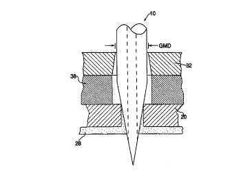
A further exemplary embodiment is shown in Figure 8 in which guide mask 32 is
spaced longitudinally from primary mask 20 by a spacer element 38. Element 38
can be
made of metal, alloy, hard plastic or other suitable material. In addition, it
need not define
a separate opening about each or any fiber tip 10 because it only performs a
spacer
function and preferably not a guide function. If desired, spacer 3 8 can be
located outside
8


CA 02291724 1999-11-26
WO 99/00687 - PCTNS98/11851
the periphery of the outermost fibers in the array, see Figure 9.
With references to Figures 9 and 10, there is shown parts of one example of a
connector that includes a fiber array holder 40 and a semiconduct device
holder 42 with
fasteners 44 that thread into female counterparts 46 in the fiber array holder
40. Holder
40 includes a keyed recess 48 that matches the keyed wafer sub-assembly 50
which secure
fiber tips 14 of fibers 10 as described above. Fibers 10 extend through a
hollow handle 52
that includes a standard fiber strain relief device 54 (shown schematically)
near the rear
end of handle 52. Epoxy or other suitable material is applied to the inner
and/or bottom
wall of recess 48 and the sub-assembly 50 inserted with precise, keyed
orientation. Once
assembly 50 is secured to holder 40, the exposed tips 14 of fibers 10 and the
forward
surface of epoxy 28 can be ground and polished, using holder 40 as a fixture
for such
operations. Once the forward surface is prepared as desired, holder 42 is
precisely fitted
to holder 40 and secured with fasteners 44. In this way, the minute
semiconductor devices
on the associate substrate within holder 42 can be precisely aligned and
juxtapositioned
with each respective facing fiber core surface 30, see Figure 6.
Alternatively, other well known mechanical means can be incorporated in a
similar
manner to orient and align the fiber array to the array of integrated
optoelectronic devices
such as detectors or to another fiber array for coupling purposes prior to
fastening the
parts mechanically.
9


CA 02291724 1999-11-26
WO 99/00687 - PCTNS98/11851
It will be understood that the drawings hereof are not necessarily drawn to
scale
and that the above mentioned "cones" or "conical" need not be exact "cones" or
"conical"
and could be pyramids or pyramidal or hybrid pyramidal-conical shapes. The
term cones
and conical are intended to include these shapes as well. Also, other changes
and
improvements can be made to the herein disclosed embodiments without departing
from
the spirit and scope of the present invention.

Representative Drawing
A single figure which represents the drawing illustrating the invention.
Administrative Status

For a clearer understanding of the status of the application/patent presented on this page, the site Disclaimer , as well as the definitions for Patent , Administrative Status , Maintenance Fee  and Payment History  should be consulted.

Administrative Status

Title Date
Forecasted Issue Date Unavailable
(86) PCT Filing Date 1998-06-05
(87) PCT Publication Date 1999-01-07
(85) National Entry 1999-11-26
Dead Application 2004-06-07

Abandonment History

Abandonment Date Reason Reinstatement Date
2003-06-05 FAILURE TO PAY APPLICATION MAINTENANCE FEE
2003-06-05 FAILURE TO REQUEST EXAMINATION

Payment History

Fee Type Anniversary Year Due Date Amount Paid Paid Date
Application Fee $300.00 1999-11-26
Maintenance Fee - Application - New Act 2 2000-06-05 $100.00 1999-11-26
Registration of a document - section 124 $100.00 2000-01-31
Maintenance Fee - Application - New Act 3 2001-06-05 $100.00 2001-05-22
Maintenance Fee - Application - New Act 4 2002-06-05 $100.00 2002-05-28
Owners on Record

Note: Records showing the ownership history in alphabetical order.

Current Owners on Record
FIBERGUIDE INDUSTRIES, INC.
Past Owners on Record
CAMLIBEL, IRFAN
RICH, ERNEST J.
RICH, THEODORE, C.
SHERMAN, JONATHAN
Past Owners that do not appear in the "Owners on Record" listing will appear in other documentation within the application.
Documents

To view selected files, please enter reCAPTCHA code :


To view images, click a link in the Document Description column. To download the documents, select one or more checkboxes in the first column and then click the "Download Selected in PDF format (Zip Archive)" or the "Download Selected as Single PDF" button.

List of published and non-published patent-specific documents on the CPD .

If you have any difficulty accessing content, you can call the Client Service Centre at 1-866-997-1936 or send them an e-mail at CIPO Client Service Centre.


Document
Description 
Date
(yyyy-mm-dd) 
Number of pages   Size of Image (KB) 
Drawings 1999-11-26 8 151
Cover Page 2000-01-25 2 77
Representative Drawing 2000-01-25 1 11
Description 1999-11-26 10 310
Abstract 1999-11-26 1 73
Claims 1999-11-26 6 183
Correspondence 2000-01-12 1 2
Assignment 1999-11-26 4 121
PCT 1999-11-26 11 371
Assignment 2000-01-31 6 290