Note: Descriptions are shown in the official language in which they were submitted.
CA 02292025 1999-12-17
~5~=~~~ ,
Magneto-Optical Recording Medium and Method for Producing Same
BACKGROUND OF THE INVENTION
The present invention relates to a magneto-optical
recording medium having a rare earth - transition metal
alloy film as a recording layer, and more particularly
to an improvement for lowering of a recording magnetic
field.
In recent years, a magneto-optical recording system
has been noticed as an overwritable high-density
recording system. The magneto-optical recording system
is such that a magnetic domain is written on a magnetic
thin film to record information by using a thermal
energy such as a semiconductor laser beam and this
information is read by utilizing a magneto-optical
effect .
A typical recording material to be used in the
magneto-optical recording system is known as a rare
earth - transition metal alloy film (which will be
hereinafter referred to as an RE-TM film) formed by
combining a rare earth element such as Gd, Tb or Dy and
a transition metal such as Fe or Co. As the magneto-
optical recording medium having the RE-TM film as a
recording layer, there has been proposed a recording
_ 1 _
~
CA 02292025 1999-12-17
medium having a four-layer structure consisting of an
Si3N4 dielectric film, TbFeCo magnetic film, SigN4
dielectric film and A1 reflecting film, for example.
In manufacturing such a magneto-optical recording
medium having the four-layer structure as mentioned
above, it is necessary to sequentially form the Si3N4
dielectric film, the TbFeCo magnetic film, the Si3N4
dielectric film and the A1 reflecting film in this order
on a substrate by sputtering or the like. In general,
the Si3N4 dielectric film is formed by RF reactive
sputtering in which an inert gas such as Ar and a
reactive gas such as N2 as a sputtering gas are
introduced into a film forming chamber.
However, in the magneto-optical recording medium to
be manufactured by the above-mentioned technique, there
is a problem such that unless recording is carried out
in an external magnetic field of 150 Oe or more, a
satisfactory CN ratio cannot be obtained. This problem
is a large obstacle in case of applying the magneto-
optical recording medium to an overwritable magnetic
field modulation system. Accordingly, the elimination
of this problem is a large subject for realizing the
magnetic field modulation system.
SUMMARY OF THE INVENTION
- 2 -
- CA 02292025 1999-12-17
It is accordingly an object of the present
invention to provide a magneto-optical recording medium
which can suppress mixing of impurities into the TbFeCo
magnetic film as a recording layer and lower a recording
magnetic field.
To achieve the above object, the present inventors
have long studied to conclude that the characteristics
are largely influenced by a degree of penetration of a
constituent element of a dielectric layer into the
TbFeCo magnetic film.
The present invention has been accomplished on the
basis of the above knowledge, and according to the
present invention, there is provided in a magneto-
optical recording medium having a substrate, a recording
layer having at least a rare earth - transition metal
alloy film formed on said substrate, and a dielectric
layer formed on said recording layer; the improvement
characterized in that a depth of an area in said
recording layer containing an element derived from said
dielectric layer is set to 70 ~ or less from an
interface between said recording layer and said
dielectric layer in a depth-directional film structure
analysis by Auger electron spectroscopy.
- 3 -
~
CA 02292025 1999-12-17
In the magneto-optical recording medium according
to the present invention, the RE-TM magnetic film is
used as a recording layer, and at least a dielectric
layer is formed on the RE-TM magnetic film.
Specifically, the present invention may be applied to a
magneto-optical recording medium having a four-layer
structure consisting of an Si3N4 dielectric film, TbFeCo
magnetic film, Si3N4 dielectric film and A1 reflecting
film.
As the RE-TM magnetic film to be used in the
present invention, all of known magnetic materials such
as TbFeCo or GdFeCo for a recording film of a
conventional magneto-optical recording medium may be
used. A film thickness of the RE-TM magnetic film is
set to about 100 - 1000 ~ from the viewpoint of
practical magneto-optical characteristics.
The recording layer may be constituted of the RE-TM
magnetic film only, or may be constituted of the RE-TM
magnetic film and a rare earth element layer such as a
Tb layer formed on the RE-TM magnetic film. The rare
earth element layer has an influence upon recording and
reproducing characteristics and enables recording and
reproduction under a low magnetic field. However, if a
film thickness of the rare earth element layer is too
- 4 -
CA 02292025 1999-12-17
large, a noise tends to increase. Accordingly, it is
preferable to set the film thickness to about 1 - 30
The dielectric layer is provided for the purposes
of improvement in corrosion resistance and enhancement
of Kerr rotation angle and Faraday rotation angle due to
multiple reflection. The dielectric layer is formed of
oxides, nitrides or oxynitrides of Si or the like or
zinc sulfide (ZnS), for example. A film thickness of
the dielectric layer is set to about 100 - 2000 ~. In
the case that the dielectric layer is laminated on the
recording layer (RE-TM film) or two of the dielectric
layers are formed on both surfaces of the RE-TM magnetic
film, the present invention is effective.
In the case that the dielectric film is laminated
on the recording layer (RE-TM magnetic film), there
occurs a phenomenon such that a constituent element of
the dielectric film penetrates into the RE-TM magnetic
film to some extent depending upon film forming
conditions.
However, such an RE-TM magnetic film containing a
constituent element of the dielectric film is not
desired in the point of characteristics, and a
proportion of such a penetration area in the RE-TM
_ 5 _
CA 02292025 1999-12-17
magnetic film largely influences a magnitude of an
external magnetic field required for recording.
In this circumstance, according to the present
invention, a depth of an area in the recording layer
containing an element derived from the dielectric layer
is set to 70 ~ or less from an interface between the
recording layer and the dielectric layer.
The interface between the recording layer and the
dielectric layer is decided by a depth-directional film
structure analysis by Auger electron spectroscopy, and
it is defined in the present invention as follows:
First, in a depth-directional Auger profile, an
average peak level of Si in case of Si3N4 dielectric
film or Zn in case of ZnS dielectric film is obtained,
and a position in the dielectric layer on the interface
side with respect to the recording layer where a peal
level of Si (or Zn) becomes 1/2 of this average peal
level is obtained.
On the other hand, an average peal level of a rare
earth element (e.g., Tb) of the RE-TM magnetic film is
obtained, and a position in the recording layer on the
interface side with respect to the dielectric layer
where a peal level of the rare earth element becomes 1/2
of this average peak level.
- 6 -
CA 02292025 1999-12-17
Finally, a middle point between the above two
positions is defined as the interface between the
recording layer and the dielectric layer.
As to the area in the recording layer containing an
element derived from the dielectric layer, this area
corresponds to an area containing N in case of Si3N4
dielectric film, and it is determined by observing a
degree of penetration of N from the interface into the
recording layer. Similarly, in case of ZnS dielectrlc
film, the area corresponds to an area containing S, and
it is determined by observing a degree of penetration of
S from the interface into the recording layer.
The setting of such a degree of penetration of the
element derived from the dielectric layer into the RE-TM
magnetic film to 70 ~ or less may be realized by
providing a blocking layer at the interface between the
dielectric layer and the recording layer.
This blocking layer is a layer having a composition
containing 3 % or more of a disiimllar element (e. g.,
oxygen) not existing in the RE-TM magnetic film. For
example, an Auger signal of oxygen to be observed
between the dielectric layer and the recording layer and
an Auger signal of Tb to be observed by an increase in
yield due to oxidation correspond to the blocking layer.
CA 02292025 1999-12-17
A film thickness of the blocking layer may be
obtained from a half width of a signal having a peak at
the interface between the dielectric layer and the
recording layer in the depth-directional Auger profile.
The blocking layer is sufficiently effective even in the
condition where an atom of the dissimilar element is
arranged. From this viewpoint, the film thickness of
the blocking layer may be several ~ or more. However,
if the film thickness of the blocking layer is too
large, the characteristics of the recording layer (RE-TM
magnetic film) is resultantly damaged, and it is
therefore preferable to set the film thickness to 100
or less in terms of the above-mentioned half width.
The formation of the blocking layer at the
interface between the dielectric layer and the recording
layer may be realized by the following manner. That is,
after forming the RE-TM magnetic film or forming a rare
earth element layer on the RE-TM magnetic film, the RE-
TM magnetic film (or the rare earth element layer) is
allowed to stand for 30 minutes or more. Alternatively,
the RE-TM magnetic film (or the rare earth element
layer) is exposed to an atmosphere having a
predetermined oxygen partial pressure or an atmosphere
having a predetermined oxygen partial pressure and a
_ g _
CA 02292025 1999-12-17
predetermined moisture partial pressure for a short
time. The oxygen partial pressure may be set to about 1
x 10'l~ - 1 x 10'1 Torr, and the steam partial pressure
may be set to about 1 x 10'1 - 1 x 10'1 Torr. By
setting the exposure time or other conditions within the
above range, the blocking layer is formed.
In manufacturing the magneto-optical recording
medium having the four-layer structure as mentioned
above, for example, the Si3N4 dielectric film of the
third layer is formed by sputtering after forming the
TbFeCo magnetic film of the second layer. Accordingly,
the TbFeCo magnetic film is allowed to stand however for
a very short time in contact with a plasma of Ar or NZ
gas as a film forming atmosphere for the Si3N4
dielectric film. Furthermore, the TbFeCo magnetic film
is exposed to Si particles sputtered.
At this time, there occurs a phenomenon such that
an active element (especially, N or N+) dissociated or
ionized in the plasma penetrates into the TbFeCo
magnetic film to cause a deterioration in
characteristics.
However, according to the present invention, a
depth of an area in the recording layer containing an
element derived from the dielectric layer is set to 70
_ g _
CA 02292025 1999-12-17
or less from the interface between the recording layer
and the dielectric layer by a preferred technique of
providing the blocking layer at the interface between
the recording layer and the dielectric layer.
Accordingly, the deterioration in characteristics can be
suppressed to enable lowering of a recording magnetic
field.
That is, a degree of penetration of the element
derived from the dielectric layer into the recording
layer is set to 70 ~i or less from the interface between
the recording layer and the dielectric layer, thereby
suppressing the deterioration in characteristics and
improving a sensitivity to an external magnetic field.
Other objects and features of the invention will be
more fully understood from the following detailed
description and appended claims when taken with the
accompanying drawings.
BRIEF DESCRIPTION OF THE DRAWINGS
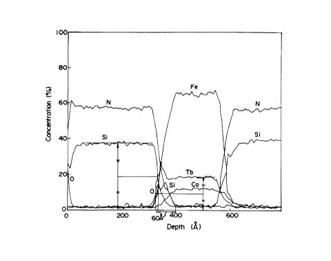
Fig. 1 is a graph illustrating an Auger profile in
Example according to the present invention having a
blocking layer;
Fig. 2 is a graph illustrating an Auger profile in
Comparison 1; and
- 10 -
CA 02292025 1999-12-17
Fig. 3 is a graph illustrating an Auger profile in
Comparison 2.
DETAILED DESCRIPTION OF THE PREFERRED EMBODIMENTS
The present invention will be more clearly
understood with reference to the following examples.
Example
In Example, a magneto-optical recording medium
having a four-layer structure consisting of an Si3N4
dielectric film, TbFeCo magnetic film, Si3N4 dielectric
film and A1 reflecting film was prepared. In this four-
layer structure, however, a Tb layer as a rear earth
element layer was formed on the surface of the TbFeCo
magnetic film. Further, a glass 2p substrate was used
as a substrate of the recording medium.
First, RF reactive sputtering was carried out by
using an Si target in an Ar atmosphere containing 20
of N2 gas under the gas pressure of 3 x 10⁻³ Torr to
form the first Si3N4 dielectric film.
Then, direct current simultaneous two-element
sputtering was carried out by using a Tb target and a
FeCo alloy target to form the TbFeCo magnetic film
having a film thickness of 225
- 11 -
CA 02292025 1999-12-17
Then, direct current sputtering was carried out by
using a Tb target to form the Tb layer having a film
thickness of 5
After forming the Tb layer, it was exposed to an
atmosphere having a moisture partial pressure of 1 x 10'
6 Torr and an oxygen partial pressure of 2 x 10'q Torr
for one minute to form a blocking layer.
Then, RF reactive sputtering was carried out again
by using an Si target to form the second Si3N4
dielectric film. Subsequently, direct current
sputtering was carried out by using an A1 target to form
the A1 reflecting film.
Finally, W curing resin was applied to the A1
reflecting film to form a protective film covering the
A1 reflecting film. Thus, a sample disk was prepared.
Comparison 1
Similarly to Example, a sample disk was prepared
with the exception that the film thickness of the TbFeCo
magnetic film was set to 230 ~ and the second Si3N4
dielectric film was formed immediately after forming the
TbFeCo magnetic film.
Comparison 2
- 12 -
CA 02292025 1999-12-17
r
Similarly to Example, a sample disk was prepared
with the exception that the second Si3N4 dielectric film
was formed immediately after forming the Tb layer.
Using the sample disks prepared above, a depth-
directional film structure analysis by Auger electron
spectroscopy was carried out. There are shown Auger
profiles of the sample disks in Figs. l to 3. Fig. 1
corresponds to Example; Fig. 2 corresponds to Comparison
1; and Fig. 3 corresponds to Comparison 2. The
conditions of the Auger electron spectroscopy were as
follows
Ion Energy: 1 kV
Emission Current: 25 mA
Measurement Area: 0.3 x 0.2 mm~
Sputter Rate: 81 /min
Acceleration Voltage: 2 kV
Beam Current: 5 x 10-~ A
Measurement Pressure: 6.8 x 10⁻⁸ Pa
Spot Radius : 30 ,um
As apparent from comparison of these Auger
profiles, it is observed in Example that a peak of
oxygen bonded to the Tb layer exists between the Si3N4
dielectric film and the TbFeCo magnetic film. This peak
of oxygen corresponds to the blocking layer, and it is
- 13 -
CA 02292025 1999-12-17
understood that the blocking layer having a film
thickness of about 50 ~ is formed.
It is also understood that a degree of nitrogen (N)
into the RE-TM magnetic film is less in Example than in
Comparison 1 and Comparison 2. More specifically, as
shown in Figs. 1 to 3, the degree of penetration from
the interface is 60 ~r in Example. To the contrary, it
is about 90 ~ in Comparison 1. Yet in Comparison 2
providing the Tb layer, it is about 80
Next, a recording and reproducing characteristic of
these sample disks by a magnetic field modulation system
was investigated. The recording and reproducing
characteristic was measured under the conditions of 1.3
m/sec of medium linear velocity, 720 kHz of recording
frequency, 4.5 mW of recording laser power and 0.6 mW of
reproducing laser power. A spectral analysis for a
whole frequency band of a reproduced waveform was
carried out with a resolution band of 10 kHz to obtain a
CN ratio in a recording external magnetic field of ~ 70
Oe. The result is shown in Table 1. As apparent from
Table 1, a magnetic field sensitivity in Example is
improved.
- 14 -
CA 02292025 1999-12-17
Table 1
Magnetic H20 ~2 Retention CN
Film Partial Partial Time Ratio
Structure Pressure Pressure
(min.) (dB)
(Tory) (Torr)
Example TbFeCo 225 1 x 10⁻⁶ 2 x 10⁻⁴ 1 48.6
+ Tb 5~
Compari TbFeCo 230. - - - 42.6
-son 1
Compari bFeCo 225 - - - 42.8
-son 2 + Tb 5~
While the invention has been described with
reference to specific embodiments, the description is
illustrative and is not to be construed as limiting the
scope of the invention. Various modifications and
changes may occur to those skilled in the art without
departing from the spirit and scope of the invention as
defined by the appended claims.
- 15 -