Note: Descriptions are shown in the official language in which they were submitted.
CA 02292442 1999-12-O1
WO 98/56101 PCT/IL98/00256
Low voltage illumination system
FIELD O~' THE INVENTION
'This invention relates to power supplies for low voltage illumination.
BACKGROUND OF THE IN3~ENTION
s Owing to the prevalence of halogen lamps, low voltage illumination is
becoming increasing popular and offers the advantage of small bright lamps
together with increased safety in the event of contact with the supply
terminals. In particular, the use of low voltage lends itself to track
lighting and
cable lighting systems, using halogen lamps or other low voltage lamps,
to which can be moved along a fixed track mounted on the ceiling so as to be
directed to those places where illumination is most required.
Various proposals for low voltage illumination are known in the art.
Most employ a transformer for transforming the high electrical supply voltage
(typically 110 V or 220 V} to a low voltage in the order of 12 V Since the
size
t s of the transformer is dependent on its power rating, such transformers are
necessarily bulky. It is therefore known in the field of a.c. illumination to
invert the incoming electrical supply voltage using a conventional rectifier
and chopper circuit so as to obtain a pulsating a.c. voltage source having a
high frequency in the order of 30 KHz. The use of high frequency permits the
2o size of the transformer to be greatly reduced.
CA 02292442 1999-12-O1
WO 98156101 PCT/IL98I00256
-2-
In one known arrangement a central transformer provides power at
low voltage (typically 12 V) to a track, rail or cable system to which Iow
voltage lamps can then be directly connected. However, it has been found that
such a proposal, although attractive, is subject to the drawback that, at high
frequency, the tracks operate like a transmission line, radiating energy. This
problem is exacerbated as the length of the track is increased, when the
inter-conductor gap is increased and when the current flow is increased. Such
drawbacks would clearly be overcome by employing a low d.c. voltage source
for feeding the tracks, but this is subject to its own problems, in particular
relating to the efficiency of rectification.
The conventional manner to produce d.c. voltage from an incoming
a.c. voltage source is to rectify the a.c. voltage using a passive rectifier
employing conventional bipolar rectifier diodes. Such diodes are typically
made from silicon having a forward bias voltage of 0.7 V Thus, the power
1 s dissipated by each rectifier diode during the half cycle that it conducts
is equal
to the product of the forward bias voltage of 0.7 multiplied by the current
passed by the diode. In a typical arrangement for energizing a series of low
voltage halogen Iamps having a combined current consumption of 25 A, the
power loss across each rectifier diode would thus amount to 17.50 W which,
2o when combined with the losses in the chopper circuit and step-down
transformer, is unacceptable.
In this regard it is to be noted that inefficient rectification of the output
not only increases operating costs but also results in heat dissipation
requiring
that the physical size of the power supply be increased. This, of course,
2s militates against the very reason for using high frequency in the first
place:
namely to reduce the size of the power s ..pply. 'T"n~refore the conventional
approach to rectification, which is widely applied in other systems, is not
suitable for halogen lighting due to the use of low voltages and hence high
CA 02292442 1999-12-O1
WO 98/56101 PCT/IL98/00256
-3-
currents and the necessity of keeping power losses down so as to enable a
small physical size.
In one popular arrangement, the low-voltage power is applied to two
uninsulated conductors in the form of cables or rigid rails to which the lamps
are attached. Such an arrangement is subject to the hazard that an
electrically
conductive short, particularly a thin wire, which is accidentally applied
between the two conductors may conduct potentially large currents. The
resultant heating of the wire constitutes a fire hazard. This situation
manifests
itself as an increase in current which may either be detected using a fuse
io which burns out when the heating effect of the current flow exceeds an
allowed threshold, by a heat-sensitive electronic device, or by a more
sophisticated current sensing element which is more directly responsive the
current flow. For example, U.S. Patent No. 5,523,653 discloses a low voltage
lighting fixture connected to an isolation step-down transformer. The fixture
i 5 is protected from limited or maximum short circuit conditions by
monitoring
the secondary current of the step-down transformer until a fault is detected,
whereupon the protection circuit de-energizes the primary of the transformer.
None of these solutions is entirely satisfactory because none operates
instantaneously when the power rating of the load connected to the supply
2o exceeds the power rating of the supply itself. Specifically, even in the
more
sophisticated case where current itself is monitored, since the supply voltage
is alternating, the current must climb from zero to the danger threshold
before
the protection element can operate. Even in this brief time interval during
the
50/60 Hz cycle, the electrically conductive short can reach dangerous
25 temperatures.
CA 02292442 2005-06-O1
72844-122
-4-
SUMMARY OF THE INVENTION
It is therefore an object of th.e invention to
provide a low voltage illumination system which addresses
the drawbacks associated with hitherto proposed low voltage
illumination systems.
According to the invention, there is provided a
low voltage illumination system, comprising:
connection terminals for connecting to a source of
low frequency a.c. voltage,
a synchronous rectifier including a pair of
MOSFETS coupled to a secondary of a step down transformer
for converting the high frequency low voltage a.c. to a low
magnitude nominally d.c. voltage, and
a pair of spaced apart conductors connected to
said low magnitude nominally d.c. voltage for connecting low
voltage lamps theretor
characterized in that:
a frequency converter is coupled to the source of
a.c, voltage for converting the low frequency a.c. voltage
to high frequency a.c. voltage,
the step down transformer is coupled to an output
of the frequency converter and includes a center tap for
driving said MOSFETS so as to produce rectified high
frequency, low voltage pulses modulated by a full wave
rectified low frequency envelope, there being negligible
dead time at each end of the rectified <~.c. half cycle
between one MOSFET switching OFF and the complementary
MOSFET switching ON, and
the pair of conductors are spaced apart.
CA 02292442 2005-11-16
72844-122
-4a-
According to the invention, there is also provided
a low voltage illumination system, comprising: a connection
unit for connecting to a source of low frequency a.c.
voltage, a frequency converter coupled to the source of a.c.
voltage for converting the low frequency a.c. voltage to a
high frequency a.c. voltage with frequency of the order of
hundreds of KHz, a planar step down transformer for
converting to high frequency, low voltage a.c., a rectifier
coupled to a secondary of the planar step down transformer
for converting the high frequency low voltage a.c. to a low
magnitude nominally d.c. voltage, and a pair of conductors
connected to said low magnitude nominally d.c. voltage for
connecting low voltage lamps thereto.
According to the invention, there is also provided
a low voltage illumination system, comprising: connection
terminals for connecting to a source of low frequency a.c.
voltage, a frequency converter coupled to the source of a.c.
voltage for converting the low frequency a.c. voltage to
high frequency a.c. voltage modulated by a full wave
rectified low frequency envelope, a step down transformer
coupled to an output of the frequency converter for
converting to high frequency, low voltage a.c., a
synchronous rectifier coupled to a secondary of the step
down transformer for converting the high frequency low
voltage a.c. to a low magnitude nominally d.c. voltage, and
a pair of conductors connected to said low magnitude
nominally d.c. voltage for connecting low voltage lamps
thereto; wherein, the synchronous rectifier includes at
least two MOSFETs, the step down transformer is coupled to
an output of the frequency converter for driving said
MOSFETs so as to produce rectified high frequency, low
voltage pulses, and a residual storage means is provided in
respect of each MOSFET for storing charge when the
CA 02292442 2005-11-16
.72844-122
-4b-
respective MOSFET is OFF so as to boost a gate-to-source
voltage thereof when the respective MOSFET is ON, in order
that the respective MOSFET remains ON for an extended time
period thereby reducing dead time at each end of the
rectified a.c. half cycle between one MOSFET switching OFF
and a complementary MOSFET switching ON.
Low voltage lamps may be directly connected to an
output of the synchronous rectifier. Alternatively, there
may be connected thereto a track comprising a pair of spaced
apart low voltage d.c. conductors for connecting low voltage
lamps thereto. Owing to the fact that the voltage across
the track conductors is d.c., there is no limit to the
spacing between the conductors which affects a.c. track
lighting systems.
Preferably, the components in the illumination
system according to the invention are provided in modules so
that each module is compatible with complementary components
made by other manufacturers. This modularity increases the
versatility of the invention.
According to a preferred embodiment, the power
supply includes a protection element directly responsive to
the impedance of the load across the
CA 02292442 1999-12-O1
WO 98/5b101 PCT/IL98/00256
-5-
supply so as to interrupt the supply immediately the load impedance exceeded
an allowed threshold. Such a protection element is designed to operate
anywhere in the a.c. current cycle thus overcoming the drawbacks with
conventional approaches.
s P~EF I~ESCI~dPTION OF THE DRAWINGS
In order to understand the invention and see how the same may be
carried out in practice, a preferred embodiment will now be described, by way
of non-limiting example only, with reference to the accompanying drawings,
in which:
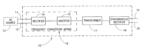
to Fig. 1 is a block diagram showing the principal functional components
of an low voltage d.c. illumination system according to the invention;
Fig. 2 is a schematic circuit diagram of a synchronous rectifier for use
with the system shown functionally in Fig. 1;
Figs. 3a to 3d are schematic representations of various voltage
15 waveforms associated with the synchronous rectifier shown in Fig. 2;
Fig. 4 is a pictorial representation of a planar transformer for use with
the system depicted in Fig. 1; and
Fig. 5~ is a schematic circuit diagram of a protection circuit for use with
the system shown functionally in Fig. 1 and responsive to the load impedance
2o across the supply for preventing overload.
DETAILED DESCRIPTION OF A PItEFEI~ED EMBODIMENT
Fig. 1 shows a low voltage illumination system designated generally as
which comprises a pair of input terminals 11 and 12 (constituting
connection means) for connecting to a source of low frequency a.c. voltage 13
2s which is shown in dotted outline since it is not itself part of the
invention. The
a.c. voltage source 13 is derived from a conventional electricity supply
feeder
having a voltage of 220/110 V and a supply frequency of 50/60 Hz. A
CA 02292442 1999-12-O1
WO 98/56101 PCT/IL98/00256
-6-
conventional rectifier 14 is coupled via the terminals 11 and 12 to the source
of a.c. voltage 13 for converting the low frequency a.c. voltage to d.c. which
is then fed to an inverter 1 ~ containing a conventional chopper circuit for
converting to high frequency a.c. at 30 _K_H?. The rectifier 14 in combination
s with the inverter 15 thus constitutes a frequency conversion means 1b for
converting the low frequency a.c. voltage to high frequency a.c. voltage.
A step down transformer 17 is coupled to an output of the frequency
conversion means 16 for converting the high frequency supply voltage of
22fl/110 V to high frequency, low voltage a.c. signal having a voltage of
to typically 12 V The step down transformer I7 is preferably implemented
using a toroidal ferrite core and the output winding is preferably implemented
using a litz (bundle of very fine insulated wires) in order to minimize losses
by reducing the leakage current due to the air gap between the primary and
secondary windings and by reducing losses due to the skin-effect and
1s proximity erect. Alternatively a higher frequency may be used and the
output
transformer implemented using a planar transformer as described below.
Although this a.c. voltage is capable of powering low voltage halogen lamps
connected to a pair of conductors coupled directly to the step down
transformer 17, this is not desirable because such conductors can behave as a
2o transmission line at high frequency resulting in significant energy loss.
This is
particularly manifest in the case where the conductors are configured as
spaced apart rails with or without insulation, such as are used in cable
lighting
systems, wherein the separation of the conductors increases the transmission
line effect.
2s To prevent the drawback associated with large high frequency currents,
the high frequency signal is recti 1 using a synchronous rectr 18 coupled
to a secondary winding {not shown) of the step down transformer 17 ~ for
converting the low voltage a.c. to low voltage d.c. A pair of conductors 19
CA 02292442 1999-12-O1
WO 98/56101 PCT/IL98/00256
and 20 are connected to the low voltage d.c. for connecting Iow voltage lamps
(not shown) thereto.
Track lighting systems peY se are known and it is therefore not
necessary to describe in detail all the components shown functionally in
s Fig. 1. Rather, with reference to Figs. 2 and 3 there will now be described
those features which are specific to the present invention and offer improved
performance over known systems.
Fig. 2 is a schematic circuit diagram of the synchronous rectifier 18
shown functionally in Fig. 1. The step down transformer 17 has a single
to primary winding 2~ rated at 120 V a.c. at 30 KHz and a secondary winding 26
having a center-tap connected to a zero voltage rail 27, and on each side of
which there are two taps connected to respective first and second voltage
rails
28a, 29a and 28b, 29b each e:chibiting a differential voltage of 12 V a.c. at
30 KHz. The circuit is symmetrical and therefore only the upper half will now
~s be described for the positive half cycle of the a.c. voltage when the upper
coil
connection {shown dotted) is positive. In this case, the voltage on the first
voltage rail 28a varies between zero and about +17V (corresponding to +12 V
(rms)) whilst the voltage on the second voltage rail 29a varies between zero
and +24 V (rms). Regardless of the instantaneous voltage on the two voltage
2o rails 28a and 29a, there exists a differential voltage therebetween of
constant
polarity and rms magnitude equal to 12 V
Connected across the first and second voltage rails 28a and 29a is a
filter comprising a resistor 30 and a capacitor 31 for filtering out high
frequency components. Connected to the junction of the resistor 30 and the
2s capacitor 31 is a capacitor 32 rated at 100nF which is connected to the
cathode of a rectifier diode 33 whose anode is connected to the first voltage
rail 28a via a current limiting resistor 34. During the positive half cycle,
the
first voltage rail 28a is at +12 V (rms) and the second voltage rail is at +24
V
(rms). Consequently, the rectifier diode 33 is reverse biased and
CA 02292442 1999-12-O1
WO 98/56101 PCT/IL98/00256
_$_
non-conducting, thereby preventing discharge of the capacitor 32 through the
resistor 34. However, during the negative half cycle, the first voltage rail
28a
is at -12 V (rms) and the second voltage rail is at -24 V (rms). Consequently,
the rectifier diode 33 is then forward biased and conducts current, thereby
charging the capacitor 32. Thus, during successive negative half cycles the
capacitor 32 accumulates charge.
Connected across the series connected rectifier diode 33 and resistor
34 is a resistor 35 and a pair of back-to-back connected Zener diodes 36 and
37 rated at 15 V which ensure that during both positive and negative half
1 o cycles, the differential output voltage thereacross never exceeds 15 V The
anode of the upper Zener diode 36 is connected to the gate terminal of a
MOSFET 38 whose source terminal is connected to the first voltage rail 28a
and whose drain terminal is connected to the I2 V d.c. output 39 of the
synchronous rectifier in parallel with the drain terminal of the complementary
15 MOSFET 40 in the lower half of the circuit.
The operation of the circuit will now be explained with reference to
the voltage waveforms shown schematically in Figs. 3a to 3d of the drawings.
Fig. 3a shows the voltage waveform at the input to the step down transformer
17 across the primary winding 25. It will be noted that the voltage across the
2o primary winding 2~ corresponds to a 30 KHz square wave pulse modulated
by a 100 Hz full wave rectified envelope. During the positive half cycle, the
voltage fed to the gate terminal of the MOSFET 38 is at approximately 24 V
(rms) less some voltage dropped across the resistor 30. The voltage fed to the
source terminal of the MOSFET 38 is nominally 12 V (rms} equal to the
25 supply voltage of the first voltage rail 28a. Consequently, there exists a
differential voltage of +12 V (rms) becweer the gate and source terminals of
the MOSFET 38 which therefore conducts current. In similar manner. there
exists a differential voltage of -12 V (rms} between the gate and source
terminals of the MOSFET 40 in the lower half of the circuit which is
CA 02292442 1999-12-O1
WO 98156101 PCT/IL98/00256
_g_
therefore cutoff. During the negative half cycle, the situation reverses and
the
upper MOSFET 38 is cutoff whilst the lower MOSFET 40 conducts, its drain
still providing the desired output of 12 V d.c.
In Fig. 3b, the full line shows the voltage waveforms on the upper first
s voltage rail 28a, whilst the dotted line shows the complementary situation
prevailing on the lower first voltage rail 28b whose voltage is in anti-phase
with the voltage on the upper first voltage rail 28a. In both cases, an
instantaneous voltage sample is shown, it being understood that just as the
voltage across the primary winding 25 of the step down transformer 17 is a
to 100 Hz modulated high frequency pulse, so too is the voltage across the
respective secondary windings of the step down transformer 17 a modulated
30 KHz pulse having a fundamental frequency of 100 Hz. Thus, the absolute
instantaneous voltages across the voltage rails 28a and 28b vary between zero
and ~ 17 V ( 12V rms).
~s Fig. 3c shows an instantaneous sample of the voltage appearing at the
output 39 of the synchronous rectifier showing successive nominally square
wave pulses derived alternately from the upper and lower MOSFETs 38 and
40. Fig. 3d shows the actual voltage waveform appearing across the output 39
of the synchronous rectifier comprising rectified 30 KHz pulses (1.e. at a
2o frequency of b0 Ku?) modulated by a full wave rectified 100 Hz envelope.
Each pulse has a duty cycle of approximately i6 ~,s, there being a dead time
of several microseconds at each end of the rectified a.c. half cycle owing to
the time between one MOSFET switching OFF and the complementary
MOSFET switching ON. If necessary, the high frequency component can be
2s suppressed using a low pass filter 41 connected between the output 39 of
the
synchronous rectifier and the zero voltage rail 27. Likewise, (although not
usually necessary when only lamps are to be connected to the system) the low
frequency 100 Hz ripple can be smoothed in known manner by means of a
capacitor 42 also connected across the output rails.
CA 02292442 1999-12-O1
WO 98/56101 PCT/IL98/00256
-10-
T'ne function of the capacitor 32 is now described. Without this
capacitor there would be a considerable dead time during which both of the
MOSFETs 3 8 and 40 would be off around the time of the zero crossing of the
low frequency power source (typically occurring at a frequency of 100Hz).
This derives from the fact that in order for either of the MOSFETs to conduct,
there must exist a gate to source voltage VGS of at least 8 V (assuming a
pinch
off voltage of approximately 4 V). This means that, under normal
circumstances, a MOSFET will remain ON only whilst the differential
voltage across the respective first and second voltage rails exceeds 8 V
1o However, in the circuit shown in Fig. 2, the capacitor 32 allows the
MOSFET to continue conducting even when the differential voltage across
the respective first and second voltage rails falls below 8 V, providing that
VGS does not fall below approximately 5 V This decrease in the dead time
between switching of the MOSFETs 38 and 40 is brought about because
during the negative half cycle when a MOSFET is OFF, the capacitor 32 in
the corresponding half of the circuit becomes charged, as explained above,
and maintains its charge because the diode 33 is reverse biased during the
subsequent positive half cycle when the MOSFET is ON. Therefore, when
VGS drops below 8 V, the capacitor 32 discharges through the MOSFET
2o which thus remains ON until the capacitor 32 fully discharges. The
capacitor
32 thus constitutes a residual storage means for storing charge during the
time
when the MOSFET is OFF so as to boost the gate-to-source voltage during
the positive half cycle when the differential voltage across the upper and
lower voltage rails becomes too low to switch the MOSFET to its ON state,
2s thereby extending the proportion of the 100Hz cycle during which the
MOSFETs are able to switch ON.
It should be noted that the output of the synchronous rectifier 18 is not
pure d.c. but has superimposed thereon a.c. harmonics having fundamental
frequencies of twice the supply frequency and of twice the inverter frequency,
CA 02292442 1999-12-O1
WO 98/56101 PCT/IL98/00256
respectively, as well as other weaker harmonics. Since the power supply is
intended for connecting to low voltage lamps, there is no need to filter out
this
harmonic component. However, if desired, additional components may be
provided within the synchronous rectifier for altering the waveform of the
s output voltage. It is thus to be understood that within the context of the
invention and the appended claims, the term "low magnitude nominally d.c.
voltage" is intended to imply a nominally d.c. voltage of Iow magnitude (i.e.
compared to the supply voltage) and of low frequency compared to the very
high frequency (30 KHz) associated with the step down transformer 17. In
other words the object of the synchronous transformer 18 is to render the
output voltage sufficiently low frequency to avoid the transmission line
radiation associated with very high frequency; whilst still allowing the use
of
very high frequency in the voltage conversion stage so as to reduce the bulk
of the step down transformer 17.
is When the MOSFET 38 conducts, its output impedance is nominally
4 mS2, whilst when it is switched off its output impedance is in the order of
several megohms. The power dissipated across the MOSFET 38, assuming an
output current of 25 A, is thus equal to I2R i.e. 625 * 4 * 10'' = 2.5 W. As
against this, if a rectifier diode having a forward bias voltage of 0.7 V or a
2o conventional bipolar junction transistor having a base-emitter voltage VBE
equal to 0.7 V were employed at the output of the synchronous transformer
18, then the power loss would be equal to 25 * 0.7 = 17.5 W. It is thus clear
that use of an active rectifier employing MOSFETs results in much higher
efficiency. This increase in efficiency is particularly important when a low
zs voltage source is employed because the lower the supply voltage, the more
significant is the junction bias voltage of a conventional rectifier or
bipolar
junction transistor. Put another way, the lower the supply voltage, the
higl~ier is
the fractional power loss across the junction, and the greater is the
advantage
of using a MOSFET as described.
CA 02292442 1999-12-O1
WO 98/56101 PCT/IL98/00256
-12-
It should be noted that in the circuit described above, the MOSFETs
switch the positive output terminal. A 24V rail is therefore needed to switch
the MOSFET as the gate voltage must be approximately lOV more positive
than the source voltage in order to switch on the MOSFET. This requires that
s fixed output taps be provided on the transformer. Alternatively the MOSFETs
may be connected to the negative output terminal thus requiring only three
output taps of 12V (rms), OV and 12V (rms) with negative phase on the
transformer eliminating taps 26 and 27. To implement such a circuit the
source and drain of each of the two MOSFETS is reversed, and the rails 29A
to and 28B and similarly 29B and 28A are unified.
It has been explained that a principal reason for converting from the
SO160 Hz low frequency associated with the electricity supply feeder to high
frequency a.c. at 30 KH? is the reduction in size of the step down transformer
which is thereby facilitated. This reduction is brought about because at high
1s frequencies, the transformer core can be replaced by a miniaturized ferrite
core assembly which can easily be accommodated in a relatively shallow
ceiling recess.
Fig. 4 is a pictorial representation showing an exploded view of a
planar transformer 50 which may used for effecting the step down
2o transformation associated with the step down transformer 17 provided the
inverter outputs a frequency substantially higher than 30 KHz and preferably
of the order of several hundred KH?. The windings of the planar transformer
50 are constructed on a multilayer printed circuit board assembly using low
thickness copper strips 51 and include leadframe windings 52 to decrease the
2s influence of skin and proximity effects, thereby allowing higher
frequencies
to be employed. Full de* :Is of a planar transformer suitable for use with the
low voltage illumination system 10 are provided in U.S. Patent No. 5,010,314
which is incorporated herein by reference. The use of such frequencies and of
planar transformers has not hitherto been considered in lighting systems due
CA 02292442 1999-12-O1
WO 98/56101 PCT/IL98/00256
-13-
to the fact that it is not customary to rectify the output of power supplies
for
lighting and, without rectification, the use of such high frequencies is
unacceptable. However the advantages offered by the use of a planar
transformer according to the invention, particularly the cheaper
s manufacturing costs, mean that such use is advantageous even if the
rectifier
is a passive diode bridge despite the large heat losses of such a rectifier.
Fig. 5 is a schematic circuit diagram of a protection circuit 55 for use
with the system shown functionally in Fig. l and responsive to the load
impedance across the supply for preventing overload. The protection circuit
io 5~ includes a comparator 56 having fed to an inverting input 57
(constituting
a first input of the comparator) a function of a supply voltage associated
with
the illumination system and having fed to a non-inverting input 58
{constituting a second input of the comparator) a function of a current flow
associated with the illumination system. To this end there is connected across
is the supply a voltage divider comprising a pair of resistors R and r whose
common junction is connected to the inverting input 57 of the comparator 56.
Likewise, the output current is fed through a sensing resistor Rs~e so that
the
voltage across the sensing resistor Rse"se is a function of the supply
current, I.
An output 59 of the comparator 56 goes from a logical LO~V level
20 (constituting a first state) to a logical HIGH level (constituting a second
state)
when a predetermined function of the impedance across the conductors falls
below a predetermined threshold R ~ Specifically, the output 59 of the
comparator 56 goes from LOW to HIGH if
v
Rsense ~
R+~
R Sense ~R + ~'~ ~ v
Rsense ~~ + Y', > ~~
CA 02292442 1999-12-O1
WO 98156101 PCTlIL98/00256
-14-
A circuit interruption device (not shown) is responsively coupled to
the output 59 of the comparator 56 for interrupting power to the pair of
conductors if the impedance falls below the predetermined threshold ~'. A
feedback resistor 60 (constituting a latching circuit) is connected between
the
s output 59 of the comparator 56 and the non-inverting input 58 of the
comparator 56 for maintaining the output 59 of the comparator 56 HIGH
regardless of a subsequent rise in impedance across the conductors. An
indication lamp 61 is connected between the output 59 of the comparator 56
and GND via a current limiting resistor 62. The indication lamp 61 constitutes
to an indication means responsive to the impedance across the conductors
falling
below the predetermined threshold for indicating an active state of the
protection circuit, during which power is interrupted to the conductors.
Clearly, in addition to, or instead of, the lamp 61, there may be provided any
other suitable audible and/or visual alarm for indicating a fault condition
t s across the conductors.
It will be appreciated that reverse logic can be applied such that the
current function is fed to the inverting input 57 and the voltage function is
fed
to the non-inverting input 58, in which case the interruption device is
operated
when the output 59 of the comparator 56 goes from HIGH to LO~V.
2o The comparator 56 thus constitutes an impedance measuring circuit
which may be incorporated within the frequency conversion means 16,
preferably between the rectifier 14 and the inverter I S or at any other
location
within the system.
In either case, the protection circuit 55 operates to interrupt power
zs immediately a short circuit or near short circuit across the output of the
power
supply regardless of where the resulting drop in output impedance is detected
in the a.c. current cycle. This is in contrast to hitherto proposed protection
circuits which are directly responsive to overcurrent detection and therefore
do not operate towards the start of the a.c. current cycle when the magnitude
CA 02292442 1999-12-O1
WO 98/56101 PCT/IL98/00256
-15-
of the current waveform is still too low to constitute an overcurrent even if
the
peak value of the waveform is indeed dangerously high.
As is known, when lamps are operated at less than their full power
rating, as when a dimmer is employed, for example, the resistance of the
lamps' filaments drops owing to the lower temperature of operation.
Therefore, if the illumination system is to be used in conjunction with
dimming devices, then in order to ensure that the reduced impedance offered
by the lamps across the conductors does not cause the protection circuit to
trip
the power supply, it is necessary that the predetermined threshold R' be less
to than the system impedance at maximum load and full dimming.
Unless steps are taken to compensate for the variation in Iamp
impedance owing to change in operation voltage, effectively less protection is
offered at full voltage operation than at reduced voltage operation. It is
therefore preferable to render the threshold R ~ variable based on the
is instantaneous value of the lamp voltage, so that if a dimming device be
employed thereby reducing the lamp voltage, maximum protection will be
offered for all settings of the dimming device. To this end, the value of any
of
the parameters R, r and Rs~~.e may be rendered dependent on the lamp voltage
appearing across the conductors. This can be done continuously by use of a
2o suitable voltage-controlled resistor such as, for example, a FET operated
in
the region before pinch-off, where the drain to source voltage VDS is small.
Alternatively, discrete control can be provided by means of a bank of equal
value resistors connected in parallel which are selectively switched in
circuit
according to the lamp voltage.
25 In order to provide the required selection, each of the resistors may be
connected in series with a corresponding MOSFET whose gate terminals are
driven by a respective threshold comparator having a threshold corresponding
to a different preset voltage. By such means, the corresponding threshold
comparator effects enabling or disabling of the resistors allowing the
CA 02292442 1999-12-O1
WO 98/56101 PCT/IL98/00256
-18-
resistance of the resistor bank to be varied as required. The number of
different resistance levels thus selectable is, of course, equal to 2N where
1~1 is
the number of resistors in the resistor bank.
It will be appreciated that the overload protection circuit 5~ is capable
s of more general application to any power supply wherein immediate overload'
protection is required in the event of a sudden drop in output impedance
owing to a short circuit or near short circuit across the output of the power
supply.
In the preferred embodiment, the synchronous rectifier is a half wave
to rectifier using only rivo MOSFETs thus requiring a center-tapped
transformer.
Alternatively, a full bridge rectifier employing four MOSFETs may be used,
thus obviating the need for a transformer with a center-tap.
It will also be appreciated that the illumination system may be
contained within a common housing having lugs or other attachment means
t s for fixing the housing to a support surface. Alternatively, the
synchronous
rectifier may be provided in a physically separate module to the frequency
conversion means and the transformer means. Such a modular approach
affords the possibility to connect a low voltage lamp to an existing high
frequency, Iow voltage a.c. source such as a so-called electronic transformer
2o via the synchronous rectifier module.