Language selection

Search

Patent 2292635 Summary

Third-party information liability

Some of the information on this Web page has been provided by external sources. The Government of Canada is not responsible for the accuracy, reliability or currency of the information supplied by external sources. Users wishing to rely upon this information should consult directly with the source of the information. Content provided by external sources is not subject to official languages, privacy and accessibility requirements.

Claims and Abstract availability

Any discrepancies in the text and image of the Claims and Abstract are due to differing posting times. Text of the Claims and Abstract are posted:

  • At the time the application is open to public inspection;
  • At the time of issue of the patent (grant).
(12) Patent: (11) CA 2292635
(54) English Title: COMPACT SPIRAL ANTENNA
(54) French Title: ANTENNE COMPACTE EN SPIRALE
Status: Expired
Bibliographic Data
(51) International Patent Classification (IPC):
  • H01Q 9/27 (2006.01)
  • H01Q 1/36 (2006.01)
  • H01Q 5/00 (2006.01)
(72) Inventors :
  • SALVAIL, GARY (United States of America)
  • YU, I-PING (United States of America)
  • MEHEN, MIKE S. (United States of America)
(73) Owners :
  • RAYTHEON COMPANY (United States of America)
(71) Applicants :
  • RAYTHEON COMPANY (United States of America)
(74) Agent: SIM & MCBURNEY
(74) Associate agent:
(45) Issued: 2002-02-19
(86) PCT Filing Date: 1999-04-01
(87) Open to Public Inspection: 1999-10-14
Examination requested: 1999-12-02
Availability of licence: N/A
(25) Language of filing: English

Patent Cooperation Treaty (PCT): Yes
(86) PCT Filing Number: PCT/US1999/007359
(87) International Publication Number: WO1999/052178
(85) National Entry: 1999-12-02

(30) Application Priority Data:
Application No. Country/Territory Date
09/054,889 United States of America 1998-04-03

Abstracts

English Abstract


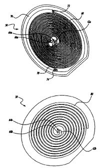
An antenna is provided that receives electromagnetic radiation and includes a
dielectric substrate (106). First and second spirals (60 and 70) on a first
surface of the substrate (106) radiate the electromagnetic radiation. A third
spiral (80) is utilized on a second surface of the substrate (106) and is
substantially underneath one of the first and second spirals (60 and 70). The
resulting spiral antenna is compact and has multioctave bandwidth capability.


French Abstract

L'invention concerne un antenne qui reçoit un rayonnement électromagnétique et comprend un substrat (106) diélectrique. Une première et une second spirale (60 et 70) disposées sur une première surface du substrat (106) diffusent le rayonnement électromagnétique. Une troisième spirale (80) est installée sur la seconde surface du substrat (106) et se trouve sensiblement sous la première ou sous la seconde spirale (60 et 70). L'antenne en spirale résultante est compacte et présente une capacité de fonctionnement sur une largeur de bande couvrant plusieurs octaves.

Claims

Note: Claims are shown in the official language in which they were submitted.


6

What is Claimed is:

1. A multiple frequency band antenna for receiving
electromagnetic radiation signals, comprising:
a dielectric substrate;
first and second spirals on a first surface of said
substrate for radiating said electromagnetic radiation
signals; and
a third spiral on a second surface of said
substrate, said third spiral being substantially
underneath one of said first and second spirals.

2. The antenna of Claim 1 wherein said antenna
operates at a predetermined wavelength, said first,
second and third spirals defining the height above a
ground plane, wherein the height above said ground plane
is less than 15 percent of said predetermined wavelength.

3. The antenna of Claim 2 wherein said antenna
operates at a predetermined wavelength, said first,
second and third spirals defining the height above a
ground plane, wherein the height above said ground plane
is less than 6 percent of said predetermined wavelength.

4. The antenna of Claim 1 wherein said antenna
operates at a predetermined wavelength, said first,
second and third spirals being disposed in a cavity of
said antenna, said first, second and third spirals
defining the height of said cavity, wherein the height of
said cavity is less than 15 percent of said predetermined
wavelength.

5. The antenna of Claim 1 wherein said antenna
operates at a predetermined wavelength, said first,


7

second and third spirals being disposed in a cavity of
said antenna, said first, second and third spirals,
defining the height of said cavity, wherein the height of
said cavity is less than 6 percent of said predetermined
wavelength.

6. The antenna of Claim 1 wherein said third
spiral has a conductor centerline, wherein said first and
second spirals are positioned so that said first spiral
is substantially positioned over the conductor centerline
of said third spiral.

7. The antenna of Claim 6 wherein said third
spiral includes a spiraling gap, said second spiral is
substantially positioned over the spiraling gap in said
third spiral.

8. The antenna of Claim 7 wherein the width of
said first and second spirals substantially matches the
width of said spiraling gap of said third spiral.

9. The antenna of Claim 1 wherein said first and
second spirals are concentric about each other and are
disposed in a common plane.

10. The antenna of Claim 1 wherein said spirals
contain copper conductor patterns etched from a copper
layer on said substrate.

11. A multiple frequency band antenna for receiving
electromagnetic radiation signals, comprising:
a dielectric substrate;


8

first and second spirals on a first surface of said
substrate for radiating said electromagnetic radiation
signals; and
a third spiral on a second surface of said
substrate, said third spiral being substantially
underneath one of said first and second spirals so as to
at least partially cover at least one of said first and
second spirals.

12. The antenna of Claim 11, wherein said antenna
operates at a predetermined wavelength, said first,
second and third spirals defining the height above a
ground plane, wherein the height above said ground plane
is less than 15 percent of said predetermined wavelength.

13. The antenna of Claim 12 wherein said antenna
operates at a predetermined wavelength, said first,
second and third spirals defining the height above a
ground plane, wherein the height above said ground plane
is less than 6 percent of said predetermined wavelength.

14. The antenna of Claim 11 wherein said antenna
operates at a predetermined wavelength, said first,
second and third spirals being disposed in a cavity of
said antenna, said first, second and third spirals
defining the height of said cavity, wherein the height of
said cavity is less than 15 percent of said predetermined
wavelength.

15. The antenna of Claim 11 wherein said antenna
operates at a predetermined wavelength, said first,
second and third spirals being disposed in a cavity of
said antenna, said first, second and third spirals


9

defining the height of said cavity, wherein the height of
said cavity is less than 6 percent of said predetermined
wavelength.

16. The antenna of Claim 11 wherein said third
spiral has a conductor centerline, wherein said first and
second spirals are positioned so that said first spiral
is substantially positioned over the conductor centerline
of said third spiral.

17. The antenna of Claim 16 wherein said third
spiral includes a spiraling gap, said second spiral is
substantially positioned over the spiraling gap in said
third spiral.

18. The antenna of Claim 17 wherein the width of
said first and second spirals substantially matches the
width of said spiraling gap of said third spiral.

19. The antenna of Claim 11 wherein said first and
second spirals are concentric about each other and are
disposed in a common plane.

20. The antenna of any one of Claims 11 to 19
wherein said spirals contain copper conductor patterns
etched from a copper layer on said substrate.

21. The antenna of any one of Claims 11 to 19
further comprising:
a balun and filter circuit connected to said first
and second spirals for removing a predetermined frequency
from said electromagnetic radiation signals.


10

22. The antenna of any one of Claims 11 to 19
further comprising:
a capacitor connected to said spirals for performing
tuning.

23. The antenna of any one of Claims 11 to 19
further comprising:
an inductor connected to said spirals for performing
tuning.

24. A multiple frequency band antenna for receiving
electromagnetic radiation signals, comprising:
a dielectric substrate;
first and second spirals on a first surface of said
substrate for radiating said electromagnetic radiation
signals; and
a third spiral on a second surface of said
substrate, said third spiral being substantially
underneath one of said first and second spirals, said
third spiral having a conductor centerline, said first
and second spirals being positioned so that said first
spiral is substantially positioned over the conductor
centerline of said third spiral so as to at least
partially cover said third spiral;
said antenna operating at a predetermined
wavelength, said first, second and third spirals defining
the height above a ground plane, wherein the height above
said ground plane is less than 15 percent of said
predetermined wavelength.

25. The antenna of Claim 24 wherein said antenna
operates at a predetermined wavelength, said first,
second and third spirals being disposed in a cavity of


11

said antenna, said first, second and third spirals
defining the height of said cavity, wherein the height of
said cavity is less than 6 percent of said predetermined
wavelength.

26. The antenna of Claim 24 wherein said third
spiral includes a spiraling gap, said second spiral is
substantially positioned over the spiraling gap in said
third spiral.

27. The antenna of Claim 26 wherein the width of
said first and second spirals substantially matches the
width of said spiraling gap of said third spiral.

28. The antenna of Claim 24 wherein said first and
second spirals are concentric about each other
and are disposed in a common plane.

29. The antenna of Claim 24 further comprising:
a capacitor connected to said spirals for performing
tuning.

Description

Note: Descriptions are shown in the official language in which they were submitted.


CA 02292635 1999-12-02
WO 99/52178 PCT/US99/07359
COMPACT SPIRAL ANTENNA
This invention relates to the field of antennas, and
more particularly to compact antennas.
BACKGROUND OF THE INVENTION
io Past approaches for antenna design include spirals that are
not sufficiently compact since their absorber cavities have
generally been on the magnitude of a quarter wavelength deep.
For example, an antenna with low frequency of 10 GHz which
has a wavelength of approximately one inch requires a cavity
i5 of at least a quarter inch in depth. Since this past approach
matches the cavity's depth to that of the longest wavelength,
it is not suitable for broadband operations.
Other past approaches for compact antennas include
utilizing patch antennas. Patch antennas are relatively thin
zo and can be on the order of 2~ of lambda (i.e., wavelength) in
thickness. However, patch antennas are limited in bandwidth
and are too large for certain applications where space is
considered a premium. Moreover, patch antennas cannot be
dedicated to multioctave bandwidths.
2s Still another previous approach is the multioctave
bandwidth spiral-mode microstrip (SMM) antenna. However, this
approach necessitates the use of a large ground plane that
extends past the diameter of the spiral arms of~the antenna in
order to operate. This large ground plane increases the
30 overall size of the antenna which may not be suitable for


CA 02292635 2001-10-16
2
applications that demand a relatively small antenna.
Moreover, the SMM antenna approach can only provide a
single common ground plane for a dual or multiple
concentric antenna configuration. This greatly limits
isolation between the antennas.
Accordingly, there is a need for a compact spiral
antenna that has multioctave bandwidth capability that
allows isolation between concentric spirals.
SUMMARY OF THE INVENTION
In accordance with the teachings of one aspect of
the present invention, an antenna is provided that
receives electromagnetic radiation and includes a
dielectric substrate. First and second spirals on a
first surface of the substrate radiate the
electromagnetic radiation. A third spiral is utilized on
a second surface of the substrate and is substantially
underneath one of the first and second spirals.
According to another aspect of the present invention
there is provided a multiple frequency band antenna for
receiving electromagnetic radiation signals, comprising:
a dielectric substrate;
first and second spirals on a first surface of said
substrate for radiating said electromagnetic radiation
signals; and
a third spiral on a second surface of said
substrate, said third spiral being substantially
underneath one of said first and second spirals so as to
at least partially cover at least one of said first and
second spirals.
According to yet another aspect of the present
invention there is provided a multiple frequency band


CA 02292635 2001-10-16
2a
antenna for receiving electromagnetic radiation signals,
comprising:
a dielectric substrate;
first and second spirals on a first surface of said
substrate for radiating said electromagnetic radiation
signals; and
a third spiral on a second surface of said
substrate, said third spiral being substantially
underneath one of said first and second spirals, said
third spiral having a conductor centerline, said first
and second spirals being positioned so that said first
spiral is substantially positioned over the conductor
centerline of said third spiral so as to at least
partially cover said third spiral;
said antenna operating at a predetermined
wavelength, said first, second and third spirals defining
the height above a ground plane, wherein the height above
said ground plane is less than 15 percent of said
predetermined wavelength.
Additional advantages and features of the present
invention will become apparent from the subsequent
description and the appended claims, taken in conjunction
with the accompanying drawings in which:
BRIEF DESCRIPTION OF THE DRAWINGS
FIG. 1 is a top view of a spiral antenna embodying
the invention;
Fig. 2 illustrates a bottom view of the spiral
antenna of FIG. 1;
FIG. 3 is an exploded isometric view of an exemplary
implementation of a mufti-band spiral antenna embodying
the invention; and


CA 02292635 2001-10-16
2b
FIG. 4 is a side exploded view of the antenna of
FIG. 3.
DETAILED DESCRIPTION OF THE PREFERRED EMBODIMENT
FIGS . 1 and 2 illustrate an exemplary embodiment of
a spiral antenna 50. Spiral antenna 50 includes
conductive material on both sides of a dielectric
substrate with first and second spirals (60 and 70 as
shown in FIG. 1) etched on one surface and a single arm
third spiral 80 etched on the


CA 02292635 1999-12-02
WO 99/52178 PCT/US99/07359
3
opposite surface (as shown in FIG. 2). The dielectric
substrate fills in the cavity formed between first/second
spirals (60 and 70) and third spiral 80.
First and second spirals (60 and 70) are positioned so that
s first spiral 60 is directly over the conductor centerline of
third spiral 80 while second spiral 70 is centered over the
spiraling gap of third spiral 80. The first and second
spirals (60 and 70) are concentric about each other and are
disposed in a common plane.
io Third spiral 80 preferably is of a greater width than the
width of either first or second spiral (60 and 70). This
greater width allows the winding arm of third spiral 80 to fit
beneath the combined width of the winding arm of first spiral
60 and the gap between the first and second spirals (60 and
i5 70). Another embodiment includes the width of the winding arm
of third spiral 80 to fit beneath the combined width of the
winding arm of second spiral 70 and the gap between the first
and second spirals (60 and 70).
First and second spirals (60 and 70) are preferably 0.020
2o inches wide with a 0.020 inch gap between them. The leg width
of third spiral 80 is 0.060 inches with a 0.02 inch gap
between successive loops. These dimensions are optimal for 2
GHz and 3 GHz operations. The spacing and widths can be
scaled for the frequency of interest. First and second spirals
2s (60 and 70) are separated from third spiral 80 by the
dielectric substrate thickness. Preferably, the thickness of
the dielectric substrate is 0.003 inches or less (thickness
values of 0.001, 0.002 and 0.003 inches can also be used).
Thicker values significantly reduce the bandwidths.
3o Due to the novel approach of the present invention, the
cavity of the spiral legs is approximately 3-5~ of the
wavelength. Consequently, when the various elements of the
antenna 50 are assembled together, the result is a compact
spiral antenna which has multioctave bandwidth capability.
s5 Moreover, it allows isolation between concentric spirals.
The third spiral 80 was conductively connected by way of a
first pad 62a with a via to either a second or third pad (64a


CA 02292635 1999-12-02
WO 99/52178 PCTNS99/07359
4
and 66a) on the same surface as first and second spirals (60
and 70) .
Tuning to reduce axial ratio is accomplished by placing a
capacitor or inductor between the pads (62a, 64a, and 66a) and
s the ground plane pads (62b, 64b, and 66b) . The ends (72 and
74) of the spiral legs are terminated with resistors and may
also be terminated with either an inductor in series or a
capacitor in parallel with the resistors. A grounding annulus
76 is provided around the spirals for attaching the
io terminating components.
FIGS. 3 and 4 illustrate an exemplary implementation of
spiral antenna 50 which embodies the invention. The spiral
antenna 50 employs filters to pass the band of one spiral and
reject the band of other spirals. When isolation is not
15 required, the filter is omitted.
FIG. 3 is an exploded isometric view of the antenna
elements, which are sandwiched between an antenna housing
structure 102 and a radome 104. Within the antenna housing
structure 102 is cavity 103 and ground plane 140. FIG. 4 is a
2o side exploded view of the elements of FIG. 3.
With reference to FIG. 4, spirals 60, 70 and 80 are defined
as copper conductor patterns etched from a copper layer on a
dielectric substrate 106. First and second spirals (60 and
70) exist in plane 105, and third spiral 80 exists in plane
25 107. Third spiral 80 notably is used to control the electric
field within antenna 50 and to direct the energy away from
antenna 50 in the direction designated by arrow 111.
In this embodiment, substrate 106 is bonded by bonding film
108 to an exposed surface of another dielectric substrate 110.
3o A ground ring 112 is defined on the opposite -surface of the
substrate 110.
A circular slab of foam 116 is bonded to ground ring 112 by
bonding film 114. Surrounding slab 116 is a conductive
isolation ring 120. A surface of a dielectric absorber slab
as structure 128 is bonded to the foam 116 by bonding film 118.
The opposite surface of the absorber 128 is bonded by bonding
film 130 to a ground plane 132 defined on a surf ace of
substrate 134. The balun and filter circuits 135 are defined


CA 02292635 1999-12-02
WO 99152178 PCT/US99/07359
on the opposite surface of the substrate 134. An exposed
surface of a dielectric substrate 138 is bonded to the surface
of the circuits 135 by bonding film 136. Another ground plane
140 is defined on the opposite side of the substrate 138.
5 More filters and baluns can be added if more spirals are
needed for multiple frequency bands.
The substrate material that exists between planes 105 and
107 of spiral antenna 50 is a low dielectric material. The
low dielectric material in the preferred embodiment includes
to polyflon from one to three mil thickness which is available
from such sources as the Polyflon company.
The next layer is a higher dielectric to increase the phase
delay of any energy passing to the ground plane 140. A
dielectric constant of approximately thirty was used. This is
backed by a conductive surface which forms the reflective
bottom of the cavity. The short coaxial feeds from the baluns
traverse the two intermediate layers to reach the two spirals
on the surface where they are attached.
Exemplary coaxial cable and termination resistor circuits
(122a and 122b) are illustrated, for connection between
termination pads connected to spiral arms on plane 105 and the
ground plane 140.
Element 126a illustrates a coaxial feed connector for
connection to the filter/balun circuits 135. Connector 126a is
for feeding spiral antenna 50.
It will be appreciated by those skilled in the art that
various changes and modifications may be made to the
embodiments discussed in the specification without departing
from the spirit and scope of the invention as defined by the
3o appended claims.

Representative Drawing
A single figure which represents the drawing illustrating the invention.
Administrative Status

For a clearer understanding of the status of the application/patent presented on this page, the site Disclaimer , as well as the definitions for Patent , Administrative Status , Maintenance Fee  and Payment History  should be consulted.

Administrative Status

Title Date
Forecasted Issue Date 2002-02-19
(86) PCT Filing Date 1999-04-01
(87) PCT Publication Date 1999-10-14
(85) National Entry 1999-12-02
Examination Requested 1999-12-02
(45) Issued 2002-02-19
Expired 2019-04-01

Abandonment History

There is no abandonment history.

Payment History

Fee Type Anniversary Year Due Date Amount Paid Paid Date
Request for Examination $400.00 1999-12-02
Registration of a document - section 124 $100.00 1999-12-02
Application Fee $300.00 1999-12-02
Maintenance Fee - Application - New Act 2 2001-04-02 $100.00 2001-03-22
Expired 2019 - Filing an Amendment after allowance $200.00 2001-10-16
Final Fee $300.00 2001-11-23
Maintenance Fee - Patent - New Act 3 2002-04-01 $100.00 2002-03-13
Maintenance Fee - Patent - New Act 4 2003-04-01 $100.00 2003-03-12
Maintenance Fee - Patent - New Act 5 2004-04-01 $200.00 2004-03-15
Maintenance Fee - Patent - New Act 6 2005-04-01 $200.00 2005-03-14
Maintenance Fee - Patent - New Act 7 2006-04-03 $200.00 2006-03-15
Maintenance Fee - Patent - New Act 8 2007-04-02 $200.00 2007-03-14
Maintenance Fee - Patent - New Act 9 2008-04-01 $200.00 2008-03-17
Maintenance Fee - Patent - New Act 10 2009-04-01 $250.00 2009-03-19
Maintenance Fee - Patent - New Act 11 2010-04-01 $250.00 2010-03-23
Maintenance Fee - Patent - New Act 12 2011-04-01 $250.00 2011-03-09
Maintenance Fee - Patent - New Act 13 2012-04-02 $250.00 2012-03-14
Maintenance Fee - Patent - New Act 14 2013-04-02 $250.00 2013-03-14
Maintenance Fee - Patent - New Act 15 2014-04-01 $450.00 2014-03-12
Maintenance Fee - Patent - New Act 16 2015-04-01 $450.00 2015-03-12
Maintenance Fee - Patent - New Act 17 2016-04-01 $450.00 2016-03-09
Maintenance Fee - Patent - New Act 18 2017-04-03 $450.00 2017-03-08
Maintenance Fee - Patent - New Act 19 2018-04-03 $450.00 2018-03-07
Owners on Record

Note: Records showing the ownership history in alphabetical order.

Current Owners on Record
RAYTHEON COMPANY
Past Owners on Record
MEHEN, MIKE S.
SALVAIL, GARY
YU, I-PING
Past Owners that do not appear in the "Owners on Record" listing will appear in other documentation within the application.
Documents

To view selected files, please enter reCAPTCHA code :


To view images, click a link in the Document Description column. To download the documents, select one or more checkboxes in the first column and then click the "Download Selected in PDF format (Zip Archive)" or the "Download Selected as Single PDF" button.

List of published and non-published patent-specific documents on the CPD .

If you have any difficulty accessing content, you can call the Client Service Centre at 1-866-997-1936 or send them an e-mail at CIPO Client Service Centre.


Document
Description 
Date
(yyyy-mm-dd) 
Number of pages   Size of Image (KB) 
Abstract 1999-12-02 1 63
Description 1999-12-02 5 242
Claims 1999-12-02 2 73
Drawings 1999-12-02 2 98
Cover Page 2000-02-03 1 55
Description 2001-10-16 7 280
Claims 2001-10-16 6 188
Cover Page 2002-01-15 2 60
Representative Drawing 2002-01-15 1 28
Representative Drawing 2000-02-03 1 23
Correspondence 2001-11-23 1 49
Correspondence 2001-05-07 1 23
Prosecution-Amendment 2001-10-16 11 332
Prosecution-Amendment 2001-11-22 1 14
Prosecution-Amendment 2000-11-20 1 30
Correspondence 2000-01-19 1 2
Assignment 1999-12-02 3 109
PCT 1999-12-02 4 138
Assignment 2000-02-15 7 407