Note: Descriptions are shown in the official language in which they were submitted.
CA 02292827 1999-12-17
- 1 -
TITLE OF THE INVENTION
INVERTER APPARATUS
BACKGROUND OF THE INVENTION
The present invention relates to an inverter
apparatus.
As a control apparatus for an AC motor such as
an induction motor subjected to variable-speed control,
a voltage-fed multiple inverter apparatus of a PWM
control scheme in FIG. 1 is known.
The apparatus shown in FIG. 1 is an inverter in
which two single-phase inverters 12 are connected in
series to form one phase, and three sets of such
single-phase inverters are star-connected. A motor 13
is driven by using output terminals U, V, and W.
In this case, a transformer 11 supplies insulated
three-phase powers to the AC input terminals of the
respective single-phase inverters. Each single-phase
inverter 12 will be described in detail with reference
to FIG. 2. Referring to FIG. 2, three-phase AC power
is converted into a DC by a three-phase bridge
rectifier 14, and the current is smoothed by a
smoothing capacitor 15. This DC is converted into
an AC by a single-phase bridge inverter 16. In this
conversion, the DC is converted into an AC of a desired
voltage and frequency by so-called PWM control.
According to the arrangement shown in FIG. 1,
an output three times higher than the voltage output
CA 02292827 1999-12-17
- 2 -
from each single-phase inverter can be obtained,
and hence a large-capacity inverter can be formed.
By shifting the PWM control timings of two single-phase
inverters constituting one phase from each other, the
PwM frequency appearing at the output terminal is
doubled. As a consequence, each voltage step is
reduced to 1/2 from the viewpoint of the overall phase,
and an output similar to a sine wave can be obtained.
In the above multiple inverter, a PWM signal can
be obtained by shifting the phases of carrier signals.
FIG. 3 shows examples of output voltage waveforms.
By alternately switching output voltages U1 and U2 from
two single-phase inverters, a waveform more similar to
a sine wave can be obtained as a whole. In addition,
by shifting the phase of the secondary winding of
the transformer 11, input harmonics can be reduced.
Consider two sets of single-phase inverters on
the upper and lower stages. Since the single-phase
inverters on each stage output three-phase power,
the power is smoothed from the viewpoint of each stage,
and a so-called "12-pulse arrangement" with the phases
of the windings of the transformer being shifted by 30°
is formed. This arrangement can reduce input harmonics.
FIG. 1 shows an example of two stages. Obviously,
however, an improved result can be obtained with three
or more stages.
However, single-phase inverters require a larger
CA 02292827 2002-04-29
-3-
number of parts than a three-phase inverter, and have
power pulsations having a frequency twice the output
frequency at the DC portion. Since the peaks of power
pulsations must be considered, the use efficiency of the
rectifier of each single-phase inverter is lower than
that of the rectifier of the three-phase inverter. In
addition, large current ripples are produced in the
smoothing capacitor of each single-phase inverter.
Furthermore, since the current ripples in the smoothing
capacitor greatly affect the service life of the
capacitor, a sufficient design margin must be ensured.
This greatly increases the cost of the inverter
apparatus.
In order to process regeneration power from a load,
DC power in all the single phase inverters must be
consumed by using resistors, or a special power
converting circuit is required, resulting in problems in
terms of both cost and size. Furthermore, as the number
of stages of single-phase inverters decreases, the input
harmonics of currents increase.
The present invention is therefore made in
consideration of the above problems, and certain
embodiments of the invention may provide an inverter
apparatus which can attain increases in the capacity and
voltage of the inverter by combining a three-phase
inverter and single-phase inverters, improve reliability
and cost performance by reducing the number of parts, and
realizing a reduction in input harmonics and a
regeneration function at a low cost.
CA 02292827 2002-04-29
-4-
BRIEF SUMMARY OF THE INVENTION
According to the first aspect of the present
invention, there is provided an inverter apparatus
comprising:
a three-phase inverter section having a three-phase
bridge rectifier for converting three-phase AC power into
DC power and a three-phase bridge inverter for converting
the DC power converted by the three-phase bridge
rectifier into three-phase AC power;
3n (n is a natural number) single-phase inverters,
of which n single-phase inverters are connected in series
with respective phase outputs of the three-phase bridge
inverter to convert three-phase AC power into DC power,
and convert the converted DC power into single-phase AC
power; and
a transformer for supplying insulated AC powers to
the three-phase inverter section and the 3n single-phase
inverters, respectively.
According to the second aspect of the present
invention, there is provided an inverter apparatus of the
first aspect,
wherein each of the single-phase inverters comprises
a rectifying section for converting the AC power supplied
from the transformer into DC power and an inverter
section for converting the DC power rectified by the
rectifying section into the single-phase AC power.
According to the third aspect of the present
invention, there is provided an inverter apparatus of the
second aspect,
wherein the AC power supplied from the transformer
is supplied to the three-phase bridge rectifier of the
CA 02292827 2002-04-29
-5-
three-phase inverter section and the rectifying section
of each of the single-phase inverters.
According to the present invention, the single-phase
inverters and the three-phase inverter are connected in
series with each other. Therefore, the arrangement
formed by combining single-phase inverters and a three-
phase inverter can decrease the number of parts as
compared with the arrangement constituted by only single-
phase inverters. In addition, since three-phase outputs
balance at the DC portion, restrictions on a smoothing
capacitor and rectifying circuit can be reduced. This
improves reliability and cost performance.
According to the fourth aspect of the present
invention, there is provided an inverter apparatus of the
first aspect,
further comprising:
a first control circuit provided for each phase to
generate a first control signal for the three-phase
bridge inverter from a reference sine signal of a
corresponding phase; and
a second control circuit provided for each phase to
generate a second control signal for controlling the
single-phase inverters so as to reduce a difference
between the first control signal, generated by the first
control circuit, and the reference sine signal of the
corresponding phase.
According to various aspects of the present
invention, each single-phase inverter supplies the
difference between a sine waveform and an output waveform
from the three-phase inverter, and a plurality of such
single-phase inverters are connected in series, a low-
voltage, high-speed switch device can be used. In
CA 02292827 2002-04-29
-6-
addition, since each single-phase inverter supplies the
difference between the sine waveform and the output
waveform from the three-phase inverter, a sine output
waveform can be obtained as a whole.
According to the fifth aspect of the present
invention, there is provided an inverter apparatus of the
first aspect,
wherein each of the single-phase inverters is used
in a bypassed state when an operation speed of the
inverter apparatus is not higher than a predetermined
speed.
According to the present invention, only the three-
phase inverter is PWM-controlled in low-speed operation,
and the remaining single-phase inverters are bypassed.
This can prevent power pulsations having a frequency
twice the output frequency in low-frequency output
operation, which poses a problem in a single-phase
inverter, reduce restrictions on the parts used, and
improve reliability
According to the sixth aspect of the present
invention, there is provided an inverter apparatus of the
first aspect,
wherein the three-phase inverter section comprises a
resistor for consuming power generated by regeneration,
the inverter apparatus further comprises a detection
circuit for detecting regeneration, and the single-phase
inverter is set in a bypassed state to make the resistor
of the three-phase inverter section consume power
generated by regeneration when regeneration is detected
by the detection circuit.
According to various aspects of the present
invention, the motor voltage is lowered in regeneration,
CA 02292827 2002-04-29
-7-
and regeneration is performed by only the three-phase
inverter or discharging is performed by a resistor, while
the remaining single-phase inverters are bypassed. This
makes it possible to perform regenerative braking of the
motor by adding only one regeneration circuit or
discharging resistor circuit.
According to a seventh aspect of the present
invention, there is provided an inverter apparatus
comprising:
3n (n is a natural number) single-phase inverters
including two or more single-phase bridge rectifiers for
converting two or more three-phase AC powers into DC
powers and a three-phase bridge inverter for converting
the DC powers converted by the three-phase bridge
rectifiers into single-phase AC power, wherein n single-
phase inverters of the 3n single phase inverts are
connected in series with respective phase outputs of the
three-phase bridge inverter, and three sets of the n
single-phase inverters are star-connected; and
a transformer for supplying insulated AC powers to
the rectifiers of the 3n single-phase inverters.
According to various aspects of the present
invention, input harmonics can be reduced satisfactorily
by multiplexing the rectifying circuits of the respective
single-phase inverters, even though the number of stages
of single-phase inverters and three-phase inverter is
small.
According to the eighth aspect of the present
invention, there is provided an inverter apparatus
comprising:
a three-phase inverter section including two three-
phase bridge rectifiers for converting two three-phase AC
CA 02292827 2002-04-29
_g_
powers into DC powers and a three-phase bridge inverter
for converting the DC powers converted by the two three-
phase bridge rectifiers into three-phase AC power;
3n (n is a natural number) single-phase inverters,
of which n single-phase inverters are connected in series
with respective phase outputs of the three-phase inverter
section to convert two three-phase AC powers into DC
powers, and convert the converted DC powers into single
phase AC power; and
a transformer for supplying insulated AC powers to
the three-phase inverter section and the 3n single-phase
inverters.
According to various aspects of the present
invention, input harmonics can be reduced satisfactorily
by multiplexing the rectifying circuits of the respective
single-phase inverters and three-phase inverter, even
though the number of stages of single-phase inverters and
three-phase inverter is small.
According to the ninth aspect of the present
invention, there is provided an inverter apparatus
comprising:
a three-phase inverter section including a three-
phase bridge rectifier for converting two three-phase AC
powers into DC powers and a three-phase bridge inverter
for converting the DC powers converted by the three-phase
bridge rectifier into three-phase AC power;
3n (n is a natural number) single-phase inverters,
of which n single-phase inverters are connected in series
with respective phase outputs of the three-phase inverter
section to convert three-phase AC power into DC power,
and convert the converted DC power into single-phase AC
power; and
CA 0229282712002-04-29
_g-
a transformer for supplying insulated AC powers to
the three-phase inverter section and the 3n single-phase
inverters.
According to various aspects of the present
invention, since the three-phase inverter has a plurality
of three-phase bridge rectifiers, input harmonics can be
satisfactorily reduced even though the number of stages
of the single-phase inverters and three-phase inverter is
small.
According to the 10th aspect of the present
invention, there is provided an inverter apparatus of the
first aspect,
further comprising a control circuit provided for
each phase to control a switching element included in the
three-phase bridge inverter of the three-phase inverter
section and a predetermined single-phase inverter at the
same switching timing.
According to the 11th aspect of the present
invention, there is provided an inverter apparatus of the
10th aspect,
wherein the control circuit controls single-phase
inverters other than the predetermined single-phase
inverter at the same switching timing.
According to various aspects of the present
invention, the switching timings of the three-phase
inverter and the predetermined single-phase inverter are
made to coincide with each other, and the switching
timings of the remaining single-phase inverters are made
to coincide with each other. This allows a control means
to be provided for each inverter group controlled at the
same switching timing, and hence can reduce the number of
parts and improve reliability.
CA 02292827 2002-04-29
y -
According to the 12th aspect of the present
invention, there is provided an inverter apparatus of the
11th aspect,
wherein the apparatus further comprises a filter
circuit provided for each phase and inserted between the
three-phase inverter and one of the n single-phase
inverters connected in series so as to remove a surge
voltage, and
wherein the single-phase inverters or the three
phase inverter section which is switched at the same
timing is connected to two ends of the filter circuit.
According to various aspects of the present
invention, surge voltages can be reduced by setting a
filter circuit at the midpoint of a series connection and
setting single-phase or three-phase inverters having the
same switching timings before and after the filter
circuit.
Additional features and advantages of the invention
will be set forth in the description which follows, and
in part will be obvious from the description, or may be
learned by practice of the invention. The features and
advantages of the invention may be realized and obtained
by means of the instrumentalities and combinations
particularly pointed out hereinafter.
BRIEF DESCRIPTION OF THE SEVERAL VIEWS OF THE DRAWING
The accompanying drawings illustrate presently
preferred embodiments of the invention, and together with
the general description given above and the detailed
description of the preferred embodiments given below,
serve to explain the principles of the invention.
CA 02292827 2002-04-29
-11-
FIG. 1 is a block diagram showing a conventional
voltage-fed multiple inverter apparatus of a PWM control
scheme;
FIG. 2 is a circuit diagram showing a single-phase
inverter of the voltage-fed multiple inverter apparatus
in FIG. 1;
FIG. 3 is a timing chart showing outputs from the
voltage-fed multiple inverter apparatus in FIG. 1;
FIG. 4 is a block diagram showing an inverter
apparatus according to the first embodiment of the
present invention;
FIG. 5 is a circuit diagram showing a three-phase
inverter in FIG. 4;
FIG. 6 is a block diagram showing an inverter
apparatus according to the second embodiment of the
present invention;
CA 02292827 1999-12-17
- 13 -
FIG. 7 is a timing chart showing operation
waveforms in the inverter apparatus according to the
second embodiment in FIG. 6;
FIG. 8 is a is a block diagram showing an inverter
apparatus according to the third embodiment of the
present invention;
FIG. 9A is a timing chart showing the operation
of the inverter apparatus according to the third
embodiment in FIG. 8 in low-speed operation;
FIG. 9B is a timing chart showing the operation
of the inverter apparatus according to the third
embodiment in FIG. 8 in high-speed operation;
FIG. 10 is a block diagram showing an inverter
apparatus according to the fourth embodiment of the
present invention;
FIG. 11 is a circuit diagram showing a three-phase
inverter in FIG. 10;
FIG. 12 is a block diagram showing an inverter
apparatus according to the fifth embodiment of the
present invention;
FIG. 13 is a circuit diagram showing a
single-phase inverter in FIG. 12;
FIG. 14 is a block diagram showing an inverter
apparatus according to the seventh embodiment of
the present invention;
FIG. 15 is a circuit diagram showing a
single-phase inverter in FIG. 14;
CA 02292827 1999-12-17
- 14 -
FIG. 16 is a block diagram showing an inverter
apparatus according to the eighth embodiment of the
present invention;
FIG. 17 is a timing chart showing the switching
operation of the inverter apparatus according to the
eighth embodiment in FIG. 16;
FIG. 18 is a block diagram showing and inverter
apparatus according to the ninth embodiment of the
present invention;
FIG. 19 is a timing chart showing the switching
operation of the inverter apparatus according to the
ninth embodiment in FIG. 18;
FIG. 20 is a graph showing a voltage waveform in
the inverter apparatus without any filter circuit;
FIG. 21 is a graph showing a voltage waveform in
the inverter apparatus having a filter circuit arranged
at the midpoint in an inverter series connection; and
FIG. 22 is a graph showing a voltage waveform in
the inverter apparatus having a filter circuit arranged
at the output terminal of an inverter.
DETAILED DESCRIPTION OF THE INVENTION
The embodiments of the present invention will be
described below with reference to the views of the
accompanying drawing.
(First Embodiment)
An inverter apparatus according to the first
embodiment will be described first with reference to
CA 02292827 1999-12-17
- 15 -
FIGS. 4 and 5.
The same reference numerals as in FIG. 1 denote
the same parts in FIG. 4, and a description thereof
will be omitted. The arrangement in FIG. 4 differs
from that in FIG. 1 in that the three single-phase
inverters on the lower stage are replaced with one
three-phase inverter 17.
As shown in FIG. 4, the inverter apparatus of
this embodiment has the three-phase inverter 17 and
single-phase inverters 12.
FIG. 5 shows the three-phase inverter 17 in detail.
A three-phase bridge rectifier 14 and smoothing
capacitor 15 in FIG. 5 are identical to those in FIG. 2,
but a three-phase bridge inverter 18 is different from
the corresponding component in FIG. 2.
As shown in FIG. 5, the three-phase inverter 17
has the three-phase bridge rectifier 14 for converting
three-phase AC power from a transformer 11 into DC
power and the three-phase bridge inverter 18 for
converting the DC power converted by the three-phase
bridge rectifier 14 into three-phase AC power.
In addition, n (n is a natural number)
single-phase inverters 12 are connected in series with
the respective phase outputs of the three-phase
inverter 17 to convert three-phase AC power into DC
power, convert the converted DC power into single-phase
AC power, and output the power. Note that the inverter
CA 02292827 1999-12-17
- 16 -
apparatus shown in FIG. 4 has one single-phase inverter
(n = 1).
In the inverter apparatus of this embodiment,
therefore, input harmonics can be reduced, and an
output waveform can be approximated to a sine wave.
In addition, the use of one three-phase inverter can
simplify the arrangement of the apparatus more than the
use of three single-phase inverters. This makes it
possible to reduce the number of parts. In addition,
in the arrangement using the single-phase inverters,
power pulsations having a frequency twice the output
frequency affect the smoothing capacitor and rectifier.
In the arrangement using the three-phase inverter,
however, no consideration is given to the above power
pulsations because the sum of the instantaneous values
of three-phase output currents is always 0.
A combination of single-phase inverters and a
three-phase inverter can therefore improve reliability
and decrease the number of parts.
(Second Embodiment)
An inverter apparatus according to the second
embodiment of the present invention will be described
next with reference to FIGS. 6 and 7.
The same reference numerals as in FIG. 4 denote
the same parts in FIG. 6, and a description thereof
will be omitted. The arrangement in FIG. 6 differs
from that in FIG. 4 in that the difference between
CA 02292827 1999-12-17
- 17 -
a reference sine signal and a signal obtained by
pulse-width-modulating the sine signal is calculated,
and each single-phase inverter is controlled by using
the signal obtained by pulse-width-modulating the
resultant difference signal.
As shown in FIG. 6, the inverter apparatus of this
embodiment differs from that of the first embodiment
in that a PWM control circuit 19 and PWM control
circuit 20 are provided for each phase.
In the embodiment having this arrangement,
each PWM control circuit 19 pulse-width-modulates
a reference sine signal a for controlling a motor 13
to output a signal b for controlling a three-phase
inverter 18. PWM control circuit 20 pulse-width-
modulates a difference signal c between the signals
a and b to output a signal d for controlling a
single-phase inverter 12.
FIG. 7 shows operation waveforms in the inverter
apparatus of this embodiment.
As shown in FIG. 7, although the switching
operation of the three-phase inverter is relatively
slow, an overall waveform can be approximated more to
a sine wave because the single-phase inverters perform
high-frequency switching. In this case, as the
operation frequency of the three-phase inverter is
decreased, a rectangular waveform can be used, and
a GTO device or the like which has a large capacity
CA 02292827 1999-12-17
- 18 -
but performs switching at a low speed can be used.
In addition, if high-speed switching devices such
as IGBTs are used as single-phase inverters, the
single-phase inverters can be easily connected in
series on two stages because the voltage of such
a device is low.
(Third Embodiment)
An inverter apparatus according to the third
embodiment of the present invention will be described
next with reference to FIGS. 8 and 9.
The same reference numerals as in FIG. 4 denote
the same parts in FIG. 8, and a description thereof
will be omitted. The arrangement shown in FIG. 8
differs from that shown in FIG. 4 in that it has PWM
control circuits 21 each serving to generate an output
voltage to only a three-phase inverter, PWM control
circuits 22 each serving to output a voltage to both
the three-phase inverter and a single-phase inverter,
and switching units 23 each serving to switch for PWM
control signals on the basis of an output frequency.
In the switching unit 23, when the output frequency is
low, switches 23a and 23b of the switching unit 23 are
turned on, whereas when the output frequency is high,
switches 23c and 23d of the switching unit 23 are
turned on. With this operation, when the driving speed
is low, each single-phase inverter is bypassed.
whether the driving speed is low is determined
CA 02292827 1999-12-17
- 19 -
as follows. For example, as shown in FIG. 8, the
rotational speed of a motor is detected by a speed
sensor 41, and the detected rotational speed is
compared with a predetermined reference speed by
a comparison circuit 42. If the detected rotational
speed is lower than the reference speed, an ON
signal is output to turn on the switches 23a and 23b.
With this operation, when the driving speed is low,
each single-phase inverter is bypassed. If the
detected rotational speed is higher than the reference
speed, an OFF signal is output to turn on the switches
23c and 23d. With this operation, when the driving
speed is high, the single-phase inverters and the
three-phase inverter are operated.
The operation of this embodiment will be described
next with reference to FIGS. 9A and 9B.
FIG. 9A shows waveforms in low-speed operation;
and FIG. 9B, waveforms in high-speed operation.
As shown in FIG. 9A, one of upper and lower
arms of the single-phase bridge inverter of each
single-phase inverter 12 is turned on to set a bypassed
state.
No low-frequency current flows in the smoothing
capacitor of each single-phase inverter, which
phenomenon is conspicuous in low-speed operation.
This prevents the service life of each capacitor from
shortening due to a reduction in ripple current and
CA 02292827 1999-12-17
- 20 -
also prevents a peak current from flowing in each
rectifier.
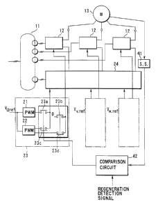
(Fourth Embodiment)
An inverter apparatus according to the fourth
embodiment of the present invention will be described
next with reference to FIGS. 10 and 11.
The same reference numerals as in FIG. 8 denote
the same parts in FIG. 10, and a description thereof
will be omitted. The arrangement shown in FIG. 10
differs from that shown in FIG. 8 in that a discharging
circuit 26, as shown in FIG. 11, having a detection
circuit 25 for detecting a DC voltage, a resistor 26b,
and a switching element 26a is added to a three-phase
inverter 24.
The detection circuit 25 detects a DC voltage in
the three-phase inverter 24 and compares the detected
DC voltage with a predetermined reference voltage.
If the detected voltage is higher than the reference
voltage, the detection circuit 25 determines that
the inverter apparatus is in a regeneration mode,
and outputs a regeneration detection signal to
the switching element 26a, a comparison circuit 42,
and the control side.
Upon reception of the regeneration detection
signal, the switching element 26a is turned on.
As a result, the resistor 26b is set in the ON state.
Upon reception of the regeneration detection signal,
CA 02292827 1999-12-17
- 21 -
the control side performs control to lower the motor
voltage to a voltage at which the motor can be driven
by only the three-phase inverter. Upon reception of
the regeneration detection signal, the comparison
circuit 42 turns on switching elements 23a and 23b to
bypass each single-phase inverter, as in the case of
low-speed operation. With this operation, the power
generated in the regeneration mode can be consumed by
only the resistor 26b of the three-phase inverter.
When the motor is to be subjected regenerative
braking, in the first embodiment shown in FIG. 4,
the detection circuit 25 and discharging circuit 26
are required for all the single-phase inverters and
three-phase inverter. In the arrangement shown in
FIG. 10, however, the detection circuit 25 and
discharging circuit 26 are provided for only the
three-phase inverter.
The operation of this embodiment will be described
next.
In this embodiment, in low-speed operation,
the motor is driven by only the three-phase inverter,
and hence the current mode directly shifts to the
regeneration mode. In high-speed operation, the motor
voltage is lowered to a voltage at which the motor
can be controlled by the three-phase inverter 24.
When regeneration is detected, the switches 23a and 23b
of the switching unit 23 are turned on, and each
i CA 02292827 1999-12-17
- 22 -
single-phase inverter 12 is bypassed. The motor is
then driven by only the three-phase inverter 24 while
the frequency is high but only the voltage is low.
The power regenerated by the motor is discharged
through the resistor 26b. With this operation,
regeneration control can be performed at several 10~
of the rated inverter power, although not at 100$ of
the rated inverter power.
Assume that GD2 is large as in the case of a fan
or the like with a square load torque. In this case,
in particular, if the method of stopping inverters
is used, the fan quickly decelerates in high-speed
operation because of the load. In low-speed operation,
however, since there is hardly any load, the stop time
is very prolonged.
This embodiment is therefore very effective
because the regeneration ability increases in low-speed
operation.
(Fifth Embodiment)
The fifth embodiment of the present invention will
be described with reference to FIGS. 12 and 13.
The same reference numerals as in FIG. 4 denote
the same parts in FIG. 12, and a description thereof
will be omitted. The arrangement shown in FIG. 12
differs from that shown in FIG. 4 in that two
rectifying circuits are connected to the inputs
of each single-phase inverter, and the winding of
CA 02292827 1999-12-17
- 23 -
the transform is doubled.
Referring to FIG. 12, a transform 27 supplies two
insulated three-phase AC powers to each single-phase
inverter. As shown in FIG. 13, each single-phase
inverter 28 has two three-phase bridge rectifiers 14.
This embodiment has 3 x m (m is a natural number)
single-phase inverters (28) each having two or more
three-phase bridge rectifiers 14 for converting two
or more three-phase AC powers into DC powers and
a three-phase bridge inverter 16 for converting the DC
powers converted by the three-phase bridge rectifiers
14 into a single-phase AC power. The m (m is a natural
number) single-phase inverters are connected in series
with each other, and three sets of m single-phase
inverters are star-connected. In the case shown in
FIG. 12, m = 2.
In the circuit in FIG. 12, the secondary winding
of the transform is twice as long as that in the
conventional inverter apparatus in FIG. 1 to set
phases of +22.5°, +7.5°, -7.5°, and -22.5°,
thereby
implementing a so-called "24-pulse rectifying circuit".
This inverter apparatus can greatly reduce input
harmonics as compared with the conventional inverter
apparatus with the 12-pulse arrangement shown in FIG. 3.
(Sixth Embodiment)
In an inverter apparatus according to the sixth
embodiment of the present invention, the number of
CA 02292827 1999-12-17
- 24 -
rectifying circuits connected to the three-phase
inverter and each single-phase inverter in the first
embodiment is increased to two.
(Seventh Embodiment)
An inverter apparatus according to the seventh
embodiment will be described with reference to FIGS. 14
and 15.
As shown FIGS. 14 and 15, this embodiment is
characterized in that a three-phase inverter has
a plurality of three-phase bridge rectifiers.
As shown in FIGS. 14 and 15, the inverter
apparatus of this embodiment has a three-phase inverter
section 17 having two three-phase bridge rectifiers 14
for converting three-phase AC power into DC power and
a three-phase inverter 18 for converting the DC power
converted by the three-phase bridge rectifiers into
three-phase AC power, 3n (n is a natural number)
single-phase inverters 12, of which n (n is a natural
number) single-phase inverters are connected in series
with the respective phase outputs of the three-phase
inverter to convert three-phase AC power into DC power,
convert the converted DC power into single-phase AC
power, and output the power, and a transform for
supplying insulated AC powers to the three-phase
inverter and 3n single-phase inverters, respectively.
In the case shown in FIG. 14, n = 1.
According to this embodiment, input harmonics
CA 02292827 1999-12-17
- 25 -
can be reduced satisfactorily by multiplexing
the rectifying circuits of the three-phase inverter,
even though the number of stages of single-phase
inverters and three-phase inverter is small.
Furthermore, in this embodiment, the number of
rectifying circuits connected to each single-phase
inverter must be increased in accordance with three
phases. In this embodiment, by adding only one
rectifying circuit to the three-phase inverter,
the same effects as those in the fifth embodiment
can be obtained. This embodiment is therefore very
effective in terms of cost performance.
(Eighth Embodiment)
An inverter apparatus according to the eighth
embodiment will be described with reference to FIGS. 16
and 17.
As shown in FIG. 16, this embodiment is comprised
of a transformer 30 connected to a three-phase AC power
supply (not shown), single-phase inverter groups 31, 32,
and 33 connected to the output side of the transformer
30, a three-phase inverter 34, and control circuits 35a,
35b, and 35c for controlling the single-phase inverter
groups 31, 32, and 33 and the three-phase inverter
group 34. A motor 13 as the load of the inverter
apparatus is connected to the output side of the
single-phase inverter group 31,
The single-phase inverter group 31 has
CA 02292827 1999-12-17
- 26 -
single-phase inverters 31a, 31b, and 31c; the
single-phase inverter group 32, single-phase inverters
32a, 32b, and 32c; and the single-phase inverter group
33, single-phase inverters 33a, 33b, and 33c. Each of
the control circuits 35a, 35b, and 35c has two PWM
circuits 36a and 36b.
The control circuits 35a and 35b will be described
next with reference to FIG. 17.
The PWM circuits 36a and 36b output pulse width
signals e, f, g, and h corresponding to a voltage
reference a.
When the signal a is at H level, an element A
(see FIG. 2) in the single-phase inverter 33a is
turned on, and an element A' (see FIG. 2) is turned off.
In contrast to this, when the signal a is at L level,
the element A is turned off, and the element A'
is turned on. Likewise, elements U and U' in the
three-phase inverter 34 are controlled by the signal e.
Elements B and B' (see FIG. 2) in the single-phase
inverter 33a are controlled by the signal f as in the
case with the signal e. Likewise, elements A and A' in
the single-phase inverters 31a and 32a are controlled
by the signal g. Elements B and B' in the single-phase
inverters 31a and 32a are controlled by the signal h.
With this control, the U-phase output voltage
waveform shown in FIG. 17 can be obtained.
In this embodiment, one PWM circuit suffices to
CA 02292827 1999-12-17
- 27 -
supply switching signals to inverters to which the same
switching timing is given. This makes it possible to
simplify the arrangement of each control circuit, and
hence a small number of parts will suffice.
(Ninth Embodiment)
An inverter apparatus according to the ninth
embodiment will be described with reference to FIGS. 18
and 19.
As shown in FIG. 18, this embodiment is comprised
of a transformer 30 connected to a three-phase AC
power supply (not shown), single-phase inverter groups
31, 32, and 33 and three-phase inverter 34 connected
to the output side of the transformer 30, control
circuits 35a, 35b, and 35c for respectively controlling
the single-phase inverter groups 31, 32, and 33 and
three-phase inverter 34, and filter circuits 37
connected between the single-phase inverter groups 32
and 33. A motor 13 as the load of the inverter
apparatus is connected to the output side of the
single-phase inverter group 31.
The filter circuits 37 of the present invention
are provided for the respective phases and inserted in
series between n single-phase inverters connected in
series and the three-phase inverter to remove surge
voltages. Single-phase inverters or three-phase
inverter which is switched at the same timing is
connected to the two ends of each filter circuit 37.
CA 02292827 1999-12-17
_ 28 _
Note that the mounting position of each filter circuit
37 need not be the midpoint position between the
single-phase inverter and the three-phase inverter.
More specifically, the filter circuit 37 may be
connected either between single-phase inverters or
between the single-phase inverter and the three-phase
inverter, while the single-phase inverter connected to
the inside (on the motor side) of the filter circuit 37
and the single-phase inverter or three-phase inverter
connected to the outside of the filter circuit 37 are
switched at the same timing.
The single-phase inverter group 31 is comprised
of single-phase inverters 31a, 31b, and 31c; the
single-phase inverter group 32, single-phase inverters
32a, 32b, and 32c; and the single-phase inverter group
33, single-phase inverters 33a, 33b, and 33c. Each of
control circuits 35a, 35b, and 35c has two PWM circuits
36a and 36b.
The control circuits 35a to 35c will be described
next with reference to FIG. 19.
The PWM circuits 36a and 36b output pulse width
signals e, f, g, and h corresponding to a voltage
reference a.
When the signal a is at H level, an element A
(see FIG. 2) in the single-phase inverter 32a is turned
on, and an element A' (see FIG. 2) in the single-phase
inverter 32a is turned off. In contrast to this, when
CA 02292827 1999-12-17
- 29 -
the signal a is at L level, the element A is turned off,
and the element A' is turned on. Likewise, elements U
and U' in the three-phase inverter 34 are controlled by
the signal e.
In addition, elements B and B' (see FIG. 2) in the
single-phase inverter 32a are controlled by the signal
f as in the case with the signal e. Likewise, elements
A and A' in the single-phase inverters 31a and 33a are
controlled by the signal g. Elements B and B' in the
single-phase inverters 31a and 33a are controlled by
the signal h.
With this control, the U-phase output voltage
waveform shown in FIG. 19 can be obtained.
In this embodiment, therefore, switching is
simultaneously performed on the inner and outer sides
of the filter circuit 37 at one switching timing.
This operation will be described in detail with
reference to FIGS. 20 to 22. FIG. 20 shows voltage
waveforms at the respective portions in a case without
any filter circuit. FIG. 22 shows voltage waveforms at
the respective portions in a case wherein a filter
circuit is set at a mounting position in the prior art.
FIG. 21 shows voltage waveforms at the respective
portions in a case wherein a filter circuit is set at
a mounting position in this embodiment.
Assume that the single-phase inverters 31 and 33
are switched at the same time. In this case, referring
CA 02292827 1999-12-17
- 30 -
to FIG. 20, reference symbol V1 denotes the sum of
the switching voltages of the single-phase inverters 31
and 33; and Vm, a voltage applied to a motor terminal.
It is known that a maximum of double surge voltage is
generated at the motor terminal owing to the stray
capacitance of the cable from the inverter to the motor
terminal.
FIG. 22 shows a case wherein the filter circuit
is connected to the output terminal of the inverter as
the conventional mounting position. Since a waveform
V1 is blunted into a waveform V2 owing to the effect of
the filter circuit, no resonance due to reflection at
the motor terminal occurs. In this case, the surge
magnification, i.e., V2max/(E31 + E33), is set to 1.5X.
FIG. 21 shows a case wherein the filter circuit is
set at the mounting position in this embodiment, i.e.,
the midpoint of the series connection of inverters.
Although filtering has an effect on switching of E33
located on the inner side of the filter circuit,
filtering has no effect on switching of E31 located on
the outer side of the filter circuit, i.e., on the load
side. For this reason, as indicated by the waveform V1,
E31 steps up, and E33 has a waveform on which the
filtering effect is exerted. With respect to this
waveform, the surge voltage at the motor terminal has
the waveform V2 because the surge voltage appears in
accordance with a step change of E31. The waveform V2
CA 02292827 1999-12-17
- 31 -
is expressed by a filter magnification of 1.5X in
FIG. 22 and a surge magnification of 2.0X in FIG. 20.
Although a voltage twice E31 is generated at the
initial portion, this voltage is equal to the sum of
E31 and E33. Thereafter, a filtering effect is exerted
on E33 to gradually raise V1, resulting in a slight
overshoot, which is 1.5 times. However, the step
amount is 1/2 the waveform shown in FIG. 22.
Obviously, therefore, the total surge voltage
is greatly lower than that generated when the filter
circuit is set at the mounting position in the prior
art.
As has been described above, according to the
present invention, the use of a three-phase inverter
can decrease the number of parts as compared with
the case wherein three single-phase inverters are used.
In addition, since three-phase outputs balance at the
DC portion, restrictions on a smoothing capacitor and
rectifying circuit can be reduced. This improves
reliability and cost performance.
Since each single-phase inverter supplies the
difference between the since waveform and the output
waveform from the three-phase inverter, a sine output
waveform can be obtained as a whole. This makes it
possible to form a three-phase inverter by using
a low-speed, large-capacity switching device, thus
improving cost performance.
CA 02292827 1999-12-17
- 32 -
Power pulsations having a frequency twice the
output frequency in low-frequency output operation,
which poses a problem in a single-phase inverter, can
be avoided. This improves reliability.
Regenerative braking of the motor can be performed
by adding only one regeneration circuit or discharging
resistance circuit.
Input harmonics can be satisfactorily reduced even
if the number of stages of single-phase inverter and
three-phase inverter is small.
Since a PWM circuit for controlling an inverter
can be omitted, reliability and cost performance can be
improved.
Surge voltages can be greatly lowered as compared
with the case wherein the filtering circuit is set at
the mounting position in the prior art.
Additional advantages and modifications will
readily occur to those skilled in the art. Therefore,
the invention in its broader aspects is not limited to
the specific details and representative embodiments
shown and described herein. Accordingly, various
modifications may be made without departing from the
spirit or scope of the general inventive concept as
defined by the appended claims and their equivalents.