Note: Descriptions are shown in the official language in which they were submitted.
CA 02292937 2000-03-06
BACKGROUND OF THE INVENTION
1. Field of the Invention
This invention relates generally to nonvolatile random access magnetic memory
devices.
i~iore particularly, the present invention relates to an improved Hall effect
ferromagnetic random
access memory cell and its method of fabrication.
2. State of the Art
The Hall effect is an electromagnetic phenomenon whereby a conductor carrying
an
electric current perpendicular to an applied magnetic field develops a voltage
gradient which is
transverse to both the current and the magnetic field. This principle has been
applied in many
electromagnetic devices, including those constructed with semiconducting
materials to produce
1 ~ field effect transistors (FETs).
FETs are well known and have been used to create digital memory devices. For
example,
U.S. Patent No. 5,29,097 to Lienau teaches a Hall effect memory device
comprising a domain
made of ferromagnetic material, substantially surrounded by a conducting coil.
When the coil is
supplied with an electric current, a residual magnetic field is created in the
domain, the polarity
of this magnetic field depending on the direction of the current of the coil.
This is how digital
information is written to the domain. A FET is disposed so as to be
perpendicularly penetrated
by this field, the differential voltage across the drains of the FET
indicating the polarity of the
magnetic field. This is how digital information is read from the domain.
While these devices are known in the art, they are somewhat difficult and
costly to
2~ construct. Additionally, fabrication constraints affect the density of
placement of the devices on
a computer chip, and thus affect the overall size of digital computer
components. It would be
Thorpe, North & Western, L.L.P.
P.O. Bor 1219
Sandy, Utah 84091-1219
Telephone: (801) 566-6633 2
CA 02292937 2000-03-06
desirable to have a hall effect ferromagnetic random access memory device that
is less expensive
and less difficult to fabricate, and which is also smaller and may be disposed
on a microchip in
greater density.
OBJECTS AND SUMMARY OF THE INVENTION
It is therefore an object of the present invention to provide a Hall effect
ferromagnetic
random access memory cell that is easier and less expensive to mass produce
than other such
devices.
It is another object of the invention to provide a Hall effect ferromagnetic
random access
memory cell that provides better signal sensing capabilities than other such
devices.
1 ~ It is another obj ect of the invention to provide a method of mass
producing such cells that
is easier and less expensive to mass produce than prior devices.
It is yet another object of the invention to provide a random access memory
circuit that is
comprised of a matrix of Hall effect ferromagnetic random access memory cells
constructed
according to this invention.
It is another object of the invention to provide Hall effect ferromagnetic
random access
memory cells that are reproducible in their behavior and give a high yield.
The above and other objects are realized in a method of manufacturing a Hall
effect
ferromagnetic non-volatile random access memory cell comprising the steps of
providing a piece
of substrate material; depositing upon the surface of the substrate a Hall
sensor material;
depositing upon the surface of the substrate interconnect lines for
electrically connecting the Hall
sensor material to its source and drains; depositing upon the Hall sensor
material and the
Thorpe, North & Western, L.L.P.
P.O. Box 1219
Sandy, Utah 84091-1219
Telephone: (80I) 566-6633
CA 02292937 2000-03-06
interconnect lines a first layer of insulating material; depositing upon the
first layer of insulating
material a thin layer of ferromagnetic material; depositing an additional
desired thickness of
ferromagnetic material upon the thin layer of ferromagnetic material; forming
the ferromagnetic
material into a magnetically polarizable domain having a long axis
substantially perpendicular or
normal to the plane of the substrate; depositing upon the ferromagnetic
material a second layer of
insulating material; depositing upon the second layer of insulating material a
thin layer of
electrically conductive material by means of electron beam deposition,
sputtering, or other thin
film deposition technique; depositing on the thin layer of electrically
conductive material an
additional desired thickness of electrically conductive material by the
process of electroplating;
forming the electrically conductive material into a coil substantially
surrounding the length of the
domain and configured to produce a residual magnetic field therein when an
electrical current is
applied to the coil; depositing upon the surface of the electrically
conductive material and the
second layer of insulating material interconnect lines for uniquely
electrically connecting the coil
to a bit write line and a word write line; and coating the entire cell
structure with a passivation
layer.
These and other objects are also realized in a Hall effect ferromagnetic non-
volatile
random access memory apparatus comprising a substrate having a plurality of
elongate,
magnetically polarizable domains oriented with their long axis substantially
normal to the
substrate. A plurality of word write lines and bit write lines are also
carried by the substrate, and
a plurality of conductive coil members are connected thereto, each between one
of the word write
2~ lines and one of the bit write lines and substantially surrounding and
being coupled to one of the
domains and having a central axis oriented substantially parallel to the long
axis of the domains.
Thorpe, North & Western, L.L.P. ,
P.O. Box 1219
Sandy Utah 84091-1219
Telephone: (801) 566-6633
CA 02292937 2000-03-06
A current source is connected to the word write lines and bit write lines for
driving a current
through a selected coil member so as to switch the residual magnetic field
direction of the
domain coupled thereto. and at least one magnetic field sensor is located
proximate to each
domain for passively sensing the direction of the residual magnetic field of
that domain.
Some of the above objects are also realized in a Hall effect ferromagnetic non-
volatile
random access memory apparatus described above wherein the sensors comprise a
field effect
transistor defining a Hall effect channel connected to a pair of drains and
oriented for
substantially perpendicular penetration of its channel by the residual
magnetic field of the
adjacent domain. The memory apparatus also has a plurality of word read lines
and bit read lines
carried by the substrate, and each of the field effect transistors are
uniquely connected with its
1 ~ source to one of the word read lines and each of its drains to one of the
bit read lines. A current
source is provided for selectively supplying a current to each of the word
read lines. A
comparator for comparing the voltage across each of the paired bit read lines
is provided to
determine the memory status of the domain.
Other objects and features of the present invention will be apparent to those
skilled in the
art, based on the following description, taken in combination with the
accompanying drawings.
BRIEF DESCRIPTION OF THE DRAWINGS
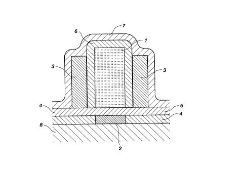
FIG. 1 provides a lateral cross section through a Hall Effect Ferromagnetic
Random
Access Memory (HFRAM) cell according to the present invention.
2~ FIG. 2 provides a lateral cross section through an alternative embodiment
of an HFRAM
cell according to the present invention in which the ferromagnetic bit lies
directly atop the sensor.
Thorpe, Yorth & Western, L.L.P.
P.O. Box 1219
Sandy, Utah 84091-1219
Telephone: (80l) 566-6633
CA 02292937 2000-03-06
FIG. 3 provides a top sectional view of a HFRAM cell according to the present
invention.
FIG. 4 provides a top view of an alternative embodiment of the sensor and
conductor
arrangement for an HFRAM cell according to the present invention.
FIG. ~ provides a lateral cross section through an alternative embodiment of
the HFRAM
cell of the present invention in which the conductors overlie rather than abut
the sensor.
FIG. 6 provides a lateral cross section through an alternative embodiment of
the HFRAM
cell of the present invention wherein the conductors overlie rather than abut
the sensor, and the
ferromagnetic bit lies directly atop the sensor.
FIG. 7 provides a lateral cross section through the HFRAM cell of FIG. 1
showing a via
emanating from the right side of the coil.
1 ~ FIG. 8 is a schematic diagram of a typical write, or storage drive, matrix
layout
interconnecting an array of HFRAM memory cells according to the present
invention.
FIG. 9 provides a schematic diagram of a typical read, or sense drive, matrix
layout
interconnecting an array of HFRAM memory cells according to the present
invention.
FIG. 10 provides a lateral cross section through an alternative embodiment of
the
HFRAM cell of the present invention wherein the ferromagnetic bit is disposed
directly on the
substrate and the sensor is disposed directly over the ferromagnetic bit.
DETAILED DESCRIPTION OF THE PREFERRED EMBODIMENT
Referring now to the drawings:
2~ FIG. 1 provides a lateral cross section through a Hall Effect Ferromagnetic
Random
Access Memory (HFRAM) cell according to the present invention. This sectional
view is taken
Thorpe, North & Western, L.L.P.
P.O. Box 1219
Sandy, Utah 84091-1219
Telephone: (801) 566-6633
CA 02292937 2000-03-06
through section B-B of FIG. 3, which provides a top sectional view of the same
HFRAM cell.
Beginning at the bottom of FIG. 1, the chip is formed on a substrate material
8 preferably
comprised of glass, silicon (Si), gallium arsenide (GaAs) or other suitable
material known in the
art. In one embodiment of the present invention, the substrate 8 may comprise
a layer of finished
integrated circuitry devices, thus providing greater component density than
other devices.
Immediately atop the substrate 8 is a Hall effect sensor 2, which is typically
connected to
four conductors 4 (two of which are visible in the sectional view of FIG. 1 )
which connect the
sensor to the sense, or read, matrix. Above the layer containing the sensor 2
and conductors 4 is
a layer of insulating material 5. This insulating material is preferably
silicon nitride (Si;N~) or
silicon dioxide (SiO,), but other suitable insulating materials known in the
art may be used. The
insulating material 5 separates the sense conductors 4 from the write, or
storage drive coil 3,
shown in cross-section in this view.
The storage drive coil 3 wraps around the ferromagnetic bit 1, with an
intervening layer
of insulating material 6 disposed therebetween. The ferromagnetic bit 1 is
preferably formed of a
ferromagnetic material selected from the group comprising iron, cobalt,
nickel, gadolinium,
indium arsenide, silicon, gallium arsenide, and indium antimonide. Other
materials known in the
art may also be suitable in accordance with the principles of this invention.
The ferromagnetic
bit is preferably oriented with its long axis approximately perpendicular to
the plane of the Hall
effect sensor (and, in this embodiment, the plane of the substrate), so as to
create a proper
magnetic flux. The ratio of the length of the domain to its width in the plane
of the substrate
2~ should be greater than 1:1, with a ratio of 2:1 or greater being
preferable. The coil is formed of a
conducting material, such as silver, copper, gold, aluminum, or other
conductive material known
Thorpe, North & Western, L.L.P.
P.O. Box 1219 '
Sandy Utah 84091-1219
Telephone: (80l) 566-6633 7
CA 02292937 2000-03-06
in the art. The insulating material 6 is preferably silicon nitride (Si;N~) or
silicon dioxide (Si02),
but other suitable insulating materials known in the art may be used. The
entire cell~structure is
overlain by an insulating cover 7, preferably made of silicon dioxide (Si02)
or silicon nitride
(Si;N,), though other materials known in the art may be advantageously used.
The wrapped configuration of the storage drive coil 3 around the ferromagnetic
bit 1 is
more clearly shown in FIG. 3, which is a top sectional view of the HFRAM cell
taken through
section A-A of FIG. 7. In this view, the coil 3 is shown overlying the bit
drive write line 10 on
one end, and having a via 9 extending out from the plane of the figure on its
other end. The coil
3 is electrically connected at the one end to the drive write line 10, and the
via 9 connects the
other end of the coil 3 to the byte drive line 15, shown more clearly in the
schematic diagram of
FIG. 8. The configuration of the bit and byte drive lines, 10 and 15, are
shown for reference
only, and in practice may be reversed from the orientation shown.
FIG. 2 provides a lateral cross section through an alternative embodiment of
an HFRANI
cell according to the present invention. The cell of this embodiment is
identical to that of FIG 1
except that the insulating layer 5 is absent, and the ferromagnetic bit 1 lies
directly atop the
sensor 2. This configuration is possible because, although the ferromagnetic
material of the bit is
conductive, it is isolated from the storage, or write, drive circuit 3 by the
insulator 6, and thus
electrically is not part of the write drive circuit. In the depiction of FIG.
2 the insulator 6 is
shown extended below the coil 3, thus electrically isolating the write drive
and read sense
circuits. This configuration provides the advantage of having the sensor 2
closer to the bit 1,
2~ which enhances the signal-to-noise ratio because the sensor is placed in
the most intense part of
the magnetic field.
Thorpe, North & Western, L.L.P.
P.O. Box 1219
Sandy Utah 84091-1219
Telephone: (80l) 566-6633
CA 02292937 2000-03-06
FIG. 4 provides a top view of an alternative embodiment of the sensor and
conductor
arrangement for an HFR.AM cell according to the present invention. This view
is taken through
section C-C of FIG. ~. This embodiment is a ''classic" Hall effect device, in
which the Hall
conductor region is comprised of indium antimonide (InSb), indium arsenide
(InAs), gallium
arsenide (GaAs), silicon (Si), or other appropriate Hall effect coefficient
material. Other forms
of sensors may also be used, including those which create variations of the
Hall effect, but in all
cases the sensing device must be capable of determining the direction or
polarity of the magnetic
field emanating from the ferromagnetic bit 1. In FIG. 4, the four conductors 4
are shown
overlapping the edge of the sensor 2, having a top connection, rather than a
butt connection as
depicted in FIGS. 1, 2, & 7. A side view of this type of configuration is
given in FIG. S. This
1 ~ configuration reduces the overall thickness of the device, and thereby
increases the allowable
density of these devices on a semiconductor chip. In FIG. 4, two of the four
conductors 4 are
shown with vias 12, depicted in such a way as to indicate that they are
extending out of the plane
of the drawing. These are in turn connected to the read sense comparator lines
19 (FIG. 9).
FIG. S provides a lateral cross section through another alternative embodiment
of the
HFRAM cell of the present invention in which the conductors 4 overlie rather
than abut the
sensor 2. As noted above, this configuration also provides manufacturing
simplicity and cost
advantages, and increases the allowable density of components on. a
semiconductor chip. The
view of FIG. 5 is taken through section D-D of FIG. 4. In this embodiment, the
sensor 2 is
approximately twice as large as its counterpart in FIGS. 1 or 2, and the sense
conductors 4
contact the sensor 2 on its top as in FIG. 4, rather than butting against it
as in FIGS. 1, 2, & 7.
The embodiment of FIG. S also includes an insulating layer 5 between the
sensor and the bit 1,
Thorpe, North & western, L.L.P.
P.O. Box 1219
Sandy, Utah 84091-1219
Telephone: (801) 566-6633 9
CA 02292937 2000-03-06
however, this insulator ~ is configured to conform to the rise caused by the
sense conductors 4.
This rise may also cause a gap 11 between the under surface of the conductors
4 and the edge of
the sensor 2, which is preferably filled with an insulating material such as
silicon nitride (Si3N:,),
or other suitable insulating material known in the art.
The unique features of the embodiments of FIG. 2 and FIG. 5 may be
advantageously
combined to provide an HFRAVI cell having all of those advantages. FIG. 6
provides a lateral
cross section through an alternative embodiment of the HFRAM cell of the
present invention
incorporating these features. The conductors 4 overlie rather than abut the
sensor 2, and the
ferromagnetic bit 1 lies directly atop the sensor 2. The principle advantages
of this configuration
are that it increases sensor sensitivity, and makes the manufacturing process
simpler and less
1 ~ costly.
FIG. 7 provides a lateral cross section through the HFRAVI cell of FIG. 1
showing a via 9
emanating from the right side of the coil 3. As noted above, the via 9
connects one end of the
coil 3 to the byte drive line 1 ~. The byte drive line 15 is shown more
clearly in FIG. 8, which
provides a schematic diagram of a typical write, or storage drive, matrix
layout interconnecting
an array of HFR.AM memory cells according to the present invention. The matrix
is in a typical
8-bit byte configuration, with bits bo through b, and bytes Bo through B". It
will be apparent to
one skilled in the art that this configuration is typical of computer memory
devices. However,
the present invention is in no way limited to devices co~gured in this manner.
The
ferromagnetic bits 1 are shown centered in reference to the write drive coils
(or loops) 3. Each
cell coil or loop 3 is interconnected electrically to the write drive matrix
through the bit drive
lines 10 and the vias 9 to the byte drive lines 15. The bit drive circuitry is
represented in this
Thorpe, North & Western, L.L.P.
P.O. Box 1219
Sandy, Utah 84091-1219
Telephone: (80l) 566-6633 1 ~
CA 02292937 2000-03-06
figure by objects 14, and the byte drive circuits are represented by objects
13. Objects 21
represent individual bit matrix select circuitry, which may be constructed in
any suitable manner
known in the art.
FIG. 9 provides a schematic diagram of a typical read, or sense drive, matrix
layout
interconnecting an array of HFRAM memory cells according to the present
invention. As above,
this matrix is also in a typical 8-bit byte configuration, with bits bo
through b, and bytes Bo
through B~. In this depiction, the sensors are "classic" Hall effect sensors,
as noted in the
discussion of FIG. 4 above, but the invention here described is not restricted
to such. The
ferromagnetic bits 1 are centered with respect to the sensors 2, and may be
disposed over the
sensors as heretofore depicted, or disposed under the sensors as depicted in
FIG. 10 (described in
more detail below). Each sensor is electrically interconnected to the read
drive matrix through
sense connectors 4. The byte row drive select lines 18 connect to each sensor
in a row through a
connector 4. When a given byte row is selected, current flows from the byte
selection and drive
circuit 17 through the line 18, the sensor 2, and thence to the common ground
20 through a
matching sensor conductor 4. In this case, the Hall voltage developed across
the sensor as a
result of the current applied across the sensor 2 by the byte drive current
and biased by the
magnetic field emanating from the ferromagnetic bit 1 is transmitted through
the second set of
sensor connectors 4 and the vias 12 to the sense lines 19 and thence to the
bit sense comparators
16, bo through b,. Line 20 connects each cell to ground.
FIG. 10 provides a lateral cross section through an alternative embodiment of
the
2~ HFR.AM cell of the present invention wherein the ferromagnetic bit 1 is
disposed directly on the
substrate 8, and the sensor 2 is disposed directly above the ferromagnetic
bit, rather than under it
Thorpe, Yorth & Western, L.L.P.
P.O. Box 1219
Sandy, Utah 8409 L-1219
Telephone: (801) 566-6633 1 1
CA 02292937 2000-03-06
as in previous depictions. All other feature relationships remain the same as
in FIGS. 1, 2, 5, 6,
and 7. As will be apparent to one skilled in the art, the memory cells of the
present invention
may be deposed over other integrated circuitry, such as other layers of HFRAM
cells, transistors,
etc., such as in a processor chip, or other circuitry requiring non-volatile
RAVI.
The HFR.AM cell of this invention is advantageously manufactured in the
following
manner. First, a piece of substantially planar substrate material is provided.
This substrate
material is preferably a conductive material. Next, a layer of insulating
material is deposited
upon the surface of the substrate. This step must be performed before the Hall
sensor material is
deposited. Upon the surface of the insulating material and substrate, a Hall
sensor material is
deposited. The Hall sensor material may be indium antimonide (InSb),
gadolinium, manganese,
1 ~ or other suitable materials. Next, interconnect lines for electrically
connecting the Hall sensor
material to its source and drains are deposited upon the surface of the
substrate wafer, and then a
first layer of insulating material is deposited upon the Hall sensor material
and the interconnect
lines.
At this point, the ferromagnetic domain must be formed on the substrate. To do
so, first,
a thin layer of ferromagnetic material is deposited upon the layer of
insulating material
mentioned above. Suitable materials for forming the domain include but are not
limited to iron,
cobalt, nickel, gadolinium, indium arsenide, silicon, gallium arsenide, and
indium antimonide.
The domain may be deposited on the substrate by any suitable thin film
deposition process, such
as electroplating, sputtering, electron beam deposition, chemical vapor
deposition, or others
known in the art. Then, an additional desired thickness of ferromagnetic
material is deposited on
this thin layer by the same process, until a ferromagnetic domain of suitable
mass is created.
Thorpe, North & Western, L.L.P.
P.O. Box 1219 '
Sandy, Utah 84091-1219
Telephone: (80l) 566-6633 12
CA 02292937 2000-03-06
S This ferromagnetic material is then shaped and formed into a magnetically
polarizable domain
having a long axis substantially perpendicular to the plane of the substrate,
so as to retain a
residual magnetic field with a magnetic flux in a desired direction exposed to
an electrical field
by the drive coil. A second layer of insulating material is then deposited
upon the ferromagnetic
domain material, and the device is ready for the application of the drive
coil.
The drive coil must be formed to substantially surround the long axis of the
Hall sensor
material. It is created in the following manner. First, a thin layer of
electrically conductive
material is deposited upon the second layer of insulating material mentioned
above. This may be
done by means of electron beam deposition or other suitable thin film
deposition techniques. An
appropriate material for forming this coil is any electrically conductive
material, preferably a
metal such as copper, silver, aluminum, or gold. After the thin layer of
conductive material is in
place, an additional desired thickness of electrically conductive material is
deposited on this thin
layer by electroplating or some other similar thin film deposition process to
obtain a sufficient
mass of conducting coil material. As with the ferromagnetic domain, the
electrically conductive
material must be formed into a coil substantially surrounding the length of
the domain, so as to
be configured to produce a residual magnetic field in the domain when an
electrical current is
applied to the coil.
After the domain and coil are completed, interconnect lines for uniquely
electrically
connecting the coil to a bit write line and a word write line are deposited
upon the surface of the
electrically conductive material and the second layer of insulating material.
To complete the cell,
2~ the entire cell structure is coated with a passivation layer as mentioned
above.
After the above steps are completed, the electrical function of the cell
structure is
Thorpe, Narth & Western, L.L.P.
P.O. Box 1219
Sandy, Utah 84091-1219
Telephone: (801) 566-6633 13
CA 02292937 2000-03-06
preferably tested to determine whether it functions properly, and the
substrate material is cut into
an appropriate size and shape for bonding each individual cell to a header. In
this way, a
plurality of cells as described herein may be interconnected to form a random
access memory
matrix as described above.
It is to be understood that the above-described arrangements are only
illustrative of the
application of the principles of the present invention. Numerous modifications
and alternative
arrangements may be devised by those skilled in the art without departing from
the spirit and
scope of the present invention and the appended claims are intended to cover
such modifications
and arrangements.
Thorpe, North & Western, L.L.P.
P.O. Box 1219
Sandy Utah 84091-1219
Telephone: (801) 566-6633 14