Note: Descriptions are shown in the official language in which they were submitted.
CA 02293497 1999-12-03
WO 98/56214 PCT/US98/11665
- 1 -
TITLE
X-RAY DETECTION SYSTEM USING ACTIVE PIXEL SENSORS
BACKGROUND OF TfiE INVENTION
Field of the Invention
This invention relates generally to a system that
detects x-rays using active pixel sensor arrays.
Discussion of the Related Art
X-ray detection has long served as a useful diagnostic
tool in a wide variety of fields. In the medical
field, for example, x-ray detection has been used to
capture images representing parts of a patient's body,
which images are then used in diagnosis and treatment.
X-rays have also long been used in bone densitometry
(i-e., the measuring of bone density). In the dental
and related fields, x-rays are used to take images of a
patient's teeth or other areas of a patient's mouth.
X-ray detection is also used in industrial fields, such
as, for example, to detect defects in pipe welds or
aircraft joints, or to perform non-destructive testing
on materials such as ceramics or glass bottles. X-ray
CA 02293497 1999-12-03
WO 98/56214 PC'T/US98/11665
- 2
detection is also used in spectroscopy, to determine
such things as the crystal spacing or particle
composition of a material under test. X-ray detection
is also used in the surveillance and security fields,
such as, f or example, in an airport luggage scanning
system. X-ray detection is used in other fields as
well.
The most conventional x-ray detection techniques use
photosensitive film to register an image. For example,
in conventional dental x-ray detection, a film
cartridge is placed in the patient's mouth. The film
is exposed to x-rays which have passed through the soft
tissue of the patient's mouth. Chemical development of
the film in the cartridge produces an image which
provides information that assists the dentist in making
a diagnosis and providing appropriate treatment.
Film is used in medical x-ray detection as well. For
example, a chest x-ray can be taken by placing a large
piece of film in front of the patient, and passing
x-rays through the patient's body from the back. Here
again, the film must be developed using chemicals to
provide an image that is useful in making a diagnosis
and providing treatment to the patient.
The drawbacks of using film to register the x-ray image
are well known. Foremost among these are the cost and
inconvenience involved in developing the film to obtain
an image. To begin with, the development process
requires the use of chemicals. Such chemicals are
expensive, troublesome to store and can also have a
negative impact on the environment. The development
process is also time consuming. The x-ray technician,
operator or physician, after exposing the film to
x-rays, must develop it in a darkroom or a closed
processor.
CA 02293497 2005-10-07
- 3 -
In dental radiography, the relatively high dosage of
radiation which the patient must receive to expose the
film sufficiently is also a major drawback. Although
the average radiation dosage per exposure using film
has been reduced over the years, the maturity of the
conventional film technology would suggest that further
significant decrease in the required dosage is
unlikely.
In view of the above problems, a number of methods of
x-ray imaging have been proposed which do not require
the use of film. Many of these systems operate by
converting the x-rays, by use of a scintillator, into
visible light, and subsequently converting the visible
light into electrical signals which can be processed by
electronic circuits to create an image on a display to
f orm an image .
In the intraoral radiography field, for example, the
pioneer patent is U.S. Patent No. 4,160,99, issued to
Dr. Robert Schwartz. Other examples include U.S.
Patent No. 5,434,418, issued to David B. Schick and
assigned to the assignee of the present application,
and U.S. Patent No. 4,987,307, issued to Giorgio Rizzo
and Cesare Gadda~
Each of these patents describes a x-ray detector which
includes a scintillator screen, and a separate and
distinct Charge-Coupled Device (CCD). The scintillator
screen converts the x-rays emerging from a radiated
tooth into visible light, while the CCD converts the
light into electrical signals. These devises, while
solving many of the problems with photographic film,
have problems inherent to their design.
CA 02293497 1999-12-03
WO 98/56214 PCT/US98/I lbb5
- 4
These problems stem from the use of a charge-coupled
device (CCD) as the image conversion device. In a CCD,
packets of electrical charges are stored in one of an
array of discrete locations (known as "pixels"), with
the amount of charge created and stored in each pixel
corresponding to the intensity of light hitting the
device at that location. The amount of charge stored
in each pixel is read out by the successive application
of control voltages to the device, which control
voltages cause the packets of charge to be moved from
pixel to pixel to a single output circuit. Through
this process, the output circuit produces an analog
electrical signal the amplitude of which at a given
point in time represents the intensity of light
incident on the device at a particular correspondence
spatial location.
A CCD relies in its operation on the transfer of
electrons from one pixel to another, a process that is
often analogized to a "bucket brigade." Accordingly,
before reaching the output circuit, the transferred
electrons must pass though silicon for macroscopic
distances, on the order of centimeters. Because of
this, the ratio of electrons successfully transferred
to the number left behind per electrode, the so-called
"charge transfer efficiency" (CTE), must be as close as
possible to perfect (i-e., no electrons left behind) to
ensure acceptable performance of the CCD.
In addition, since net CTE varies exponentially with
the number of charge transfers, the requirement for
transfer efficiency becomes more stringent as CCD array
sizes become larger. Also, manufacturing yield may
decrease as the array size increases, since CCDs are
vulnerable to single point defects that can block an
entire column, rendering the entire device unusable.
CA 02293497 1999-12-03
WO 98/56214 PCT/US98/11665:
- 5 -
CCDs also require special manufacturing techniques to
achieve the required high CTE. As a result of the
necessity of using such techniques, CCDs are not
integratable with low power CMOS circuits, the
technology most appropriate for low power integration
of on-chip timing and driver electronics that is
required for instrument miniaturization. Moreover,
since CCDs require 12-26 volts of power, devices using
this technology can present something of a shock
hazard.
Other devices have also been used as the image
conversion device in lieu of CCDs. For example, U.S.
Patent No. 5,043,582 to Cox et al, describes an x-ray
imaging system constructed from a light sensitive
dynamic random access memory (DRAM). The device is
non-monolithic, consisting of a first layer of light
sensing elements (a bifocal plane array") and a second
layer of transistors for reading out data from the
light sensing elements, with the layers interconnected
with indium bump bonds. The non-monolithic nature of
these structures, however, inherently causes a number
of problems. To begin with, the fabrication processes
for such devices are very complex and low yielding,
making the systems expensive to produce. Further, the
separate layers thermally expand and contract at
different rates, resulting in reliability problems with
the device. In addition, the passive nature of these
devices (i.e., the absence of an active transistor
within the pixel unit cell) results in a high readout
noise.
X-ray sensor arrays have also been made of amorphous
silicon. Such devices comprise generally an array of
amorphous photodiodes, and an array of thin-film
transistors which select the photodiodes that are to be
read out. Such devices, however, are passive, and,
CA 02293497 2005-10-07
6
like the system described in the Cox et al. patent,
suffer From high readout noise. In addition, there are
limitations as to how small pixels in non-monolithic
devices can be made, since advanced photo-lithographic
techniques cannot be used. These pixel size
limitations in turn limit the resolution that can be
achieved.
Recently, Active Pixel Sensor (APS) technology has
provided an alternative to CCDs and other sensing
devices for converting light into electrical signals.
This technology is shown, for example, in U.S. Patent
No. 5,4?1,515 to Fossum et al. In general terms, an
APS array is defined as an array of light sensors having
one or more active transistors associated with each pixel.
The transistors, which are the pixel's "active" elements,
perform gain or buffering functions.
Because each pixel has its own active element, the
charges that collect below each photosite need not be
transferred through a "bucket brigade" during the
readout period, as in a CCD. Thus, the need for nearly
perfect charge transfer is eliminated. Accordingly, an
APS array does not exhibit the negative attributes
associated with charge transfer across macroscopic
distances required by the CCD.
Also, since APS devices can be manufactured using
standard C'MOS techniques, the array can operate on 5
volt power, minimizing the shock hazards of the device.
An additional advantage of utilizing APS technology in
x-ray applications is that CMOS wafers are made in much
larger diameter than are CCD wafers. This would allow
for the manufacture of very large devices for other
radiology applications, such as mammography,
fluoroscopy, orthopedics, etc.
CA 02293497 1999-12-03
WO 98/56214 PCTlUS98/11665
While APS arrays have of late enjoyed a good deal of
attention from those constructing light detecting
devices -- such as in the high definition television
(HDTV) and electronic still camera fields -- they have
not heretofore been used to construct an x-ray
detector. The reasons for this are several. To begin
with, an x-ray detector is generally constructed by
disposing a scintillator on top of a light sensing
device, so that the scintillator first converts
incident x-rays into visible light, and the light
sensing device in turn converts the visible light into
electrical signals. Some fraction of the x-rays that
enter the scintillator, however, will invariably exit
the scintillator and impinge upon the light sensing
device. Such unconverted x-rays would be registered by
conventional APS devices, and cause spurious signals to
be created, which would, in turn, result in a noisy
image.
In addition, the visible light emitted by scintillators
is typically in the blue-green portion of the visible
spectrum. APS arrays, however, are widely believed to
exhibit a very poor response to blue-green light,
leading in turn to the belief that APS arrays are not
suitable for use in x-ray detectors.
Another problem with x-ray detectors is event
detection. Since x-ray detectors are generally
manufactured separately from, and not synchronized
with, the source of x-rays, the x-ray detector must
have some mechanism for determining when it has been
exposed to x-ray rays, so that it knows when to read
out the data. This problem does not exist with the
devices such as digital cameras, since the visible
radiation which cameras sense is either always present
or is provided from a flash that is synchronized with
the operation of the camera.
CA 02293497 2005-10-07
8
Also, APS devices have a higher dark signal (ile.,
thermally generated currents produced by the device
when not exposed to radiation) than CCDs, since the
dark signal in CCDs can be significantly reduced by
operating the device in the multi-phase pinned (MPP)
mode. This is believed to make APS arrays less
suitable as x-ray detectors than as light detectors.
In particular, because scintillators emit a much
smaller number of photons than are present in a light
sensing environment (such as, for example, a
photography environment), the dark signal is believed
to be more problematic in an x-ray detector, since the
dark signal, if not corrected for, will have a greater
imgact on the signal-to-noise ratio.
Furthermore, it has been t!~eorized that CMOS
transistors, which are the type used in constructing
APS devices, are more susceptible to damage and noise
generation from high frequency radiation such as x-rays
than the MOS transistors used in CCDs. Still further,
it has been theorized that large APS arrays will have
poor manufacturing yields.
There is a need, therefore, for a new type of x-ray
detector that solves the problems of conventional x-ray
detectors by exploiting APS technology, while at that
same time overcoming the real and perceived drawbacks
associated with using APS arrays to detect x-rays.
SUI~ARY OF THFs INVENTION
One feature of an embodiment of the present invention is to
provide an x-ray detector which does not exhibit the
disadvantages of CCDs or the other image conversion devices
discussed above.
CA 02293497 2005-10-07
_ g _
Another feature of the preferred embodiments of the present
invention is to provide an x-ray detector that utilizes APS
technology.
Another feature of a preferred embodiment of the present
invention is to provide an x-ray detector in which the active
pixel sensors and circuitry for reading out the active pixel
sensors are monolithically formed on a semiconductor
substrate.
In accordance with one aspect of the present invention, an x-
ray detector is provided that includes a scintillator that
converts an invisible-radiant-energy image into a visible-
light image, and a sensor array that converts the visible-
light image into an electrical signal, the sensor array
comprising a plurality of CMOS active pixel sensors.
IS In accordance with another feature of preferred embodiments of
the present invention, each active pixel sensor includes a
photogate electrode, a transfer gate electrode, a reset
electrode and a semiconductor channel underlying the
electrodes.
In accordance with yet another feature of the preferred
embodiments of the present invention, each active pixel sensor
includes a transfer gate electrode, a reset electrode and a
semiconductor channel underlying the electrodes, the
semiconductor channel including a photodiode formed by a p-n
junction.
In accordance with yet another preferred embodiment of the
present invention, the semiconductor channel is formed in a
shallow n-type well or p-type well on the top of the
semiconductor substrate.
In accordance with still another preferred embodiment of the
present invention, a method of reading out data from an x-ray
detector is provided that includes the steps of
CA 02293497 1999-12-03
WO 98/56214 PCT/US9R/11665
- 10 -
continuously reading out frames of data from the x-ray
detector, and determining whether the x-ray detector
was exposed to x-rays by examining each read out frame
of data .
BRIEF DESCRIPTION OF THE DRAWINGS
Fig. 1 is an isometric view of the x-ray detector of
the present invention.
Fig. 2A is a magnified cross sectional view of one
embodiment of the x-ray detector shown in Fig. 1, taken
from section line 3--3.
Fig. 2B is a magnified cross sectional view of another
embodiment of the x-ray detector shown in Fig. 1, taken
from section line 3--3.
Fig. 2C is a magnified cross sectional view of yet
another embodiment of the x-ray detector shown in Fig.
1, taken from section line 3--3.
Fig. 3A is an illustration of an n-well structure
according to one embodiment of the present invention.
Fig. 3B is an illustration of a p-well structure
according to another embodiment of the present
invention.
Fig. 3C is an illustration of an n-well structure
according to yet another embodiment of the present
invention.
Fig. 4A is a schematic diagram of an active pixel
sensor array according to one embodiment of the present
invention.
CA 02293497 1999-12-03
WO 98/56214 PCT/US98/11665
- 11 -
Fig. 4H is a schematic diagram of an active pixel
sensor array according to another embodiment of the
present invention.
Fig. 5 is a time line illustrating a method for reading
out from an x-ray detector according to one embodiment
of the present invention.
Fig. 6A is a schematic diagram illustrating one
embodiment of the x-ray detector of the present
invention being utilized in a computerized diagnostic
system.
Fig. 6H is a schematic diagram illustrating another
embodiment of the x-ray detector of the present
invention being utilized in a computerized diagnostic
system.
Fig. 7 is an illustration of the x-ray detector of the
present invention being connected to a small radio
transmitter.
DETAILED DESCRIPTION OF THE PREFERRED EMBODIMENT
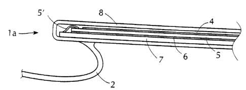
Fig. 1 depicts in a very general manner the x-ray
detector of the present invention. The detector 1 is
connected to a cable 2, which transmits the electrical
signals generated by the x-ray detector to peripheral
processing circuitry (not shown) which may, by way of
example, be integrated with a personal computer (also
not shown).
Figs. 2A-2C are magnified cross sectional views of
three embodiments of the x-ray detector of Fig. 1,
taken from section line 3--3. In the embodiment shown
in Fig. 2A, the x-ray detector includes a scintillator
4 on top of a semiconductor 5 on top of a tungsten
CA 02293497 1999-12-03
WO 98/56214 PCT/US98/1160_>
12 -
layer 6, all supported on a passivated ceramic
substrate 7. In general terms, the scintillator 4
converts x-rays into visible light, while the
semiconductor 5, in turn, converts the light into
electrical signals representing the image. The
tungsten layer 6 absorbs any x-rays which were not
converted by the scintillator 5 to those x-rays from
hitting the patient, and absorbs any backscattered
radiation. The semiconductor 5 comprises a large area
semiconductor image array of APS pixels and an
integrated signal amplifier converted. The electrical
signals produced by the semiconductor 5 are conveyed to
the cable 2 via conductive lead 5'. The conductive
lead 5' may also convey electrical power and control
signals from the computer to the semiconductor 5. The
entire x-ray detector is enclosed in a protective
aluminum enclosure 8, pervious to x-ray radiation,
which protects the x-ray detector from shock and
enables it to be moisture resistant.
The scintillator layer 4 is interposed between the
x-ray source and the semiconductor layer 5, to both
protect the semiconductor from unwanted x-ray exposure
and to provide conversion of the x-rays to visible
light for direct detection by the semiconductor. The
scintillator layer may be composed of gadolinium
oxysulphate (GDZSOS) or thallium-doped cesium iodide
(CsI(T1)). Each of these materials is sensitive to
x-ray photons, and efficiently converts them into
visible photons in the 500-600 ~m range. Other x-ray-
to-light converting materials that may be used for the
scintillator include cadmium telluride, cadmium
sulfide, calcium tungstate (CaW04), zinc sulfide and
zinc cadmium sulfide. Scintillating glass, such as for
example terbium glass, or scintillating optical fibers
may also be used. The scintillator 4 is positioned to
CA 02293497 1999-12-03
WO 98/56214 PCTNS98/11665
- 13 -
be directly exposed to the x-rays which readily pass
through the protective aluminum enclosure 8.
In x-ray imaging, as discussed above, the x-rays are
first converted into visible light by the scintillator.
However, as also discussed above, the scintillator will
not convert 100% of the x-rays that it receives; some
x-rays will inevitably pass through the scintillator
unconverted. Such unconverted x-rays cause a very
large local charge which, if registered by the pixels,
can create noise and dark spots in the resultant image.
One way to limit the unconverted x-rays from being
registered by the APS array is to interpose a fiber
optic faceplate between the scintillator 4 and the
semiconductor 5. This embodiment is illustrated in
Fig. 2H, which includes a fiber optic faceplate 9
between the scintillator 4 and the semiconductor 5.
The fiber optic faceplate will absorb a good portion of
the unconverted x-ray before they reach the APS array.
Another technique is to use scintillating fibers, which
fibers absorb x-rays and emit visible light
corresponding in intensity to the intensity of the
x-rays. This embodiment is illustrated in Fig. 2C,
which does not include a scintillator, but instead
includes a scintillating fiber optic faceplate 11 on
top of the semiconductor 5. In this embodiment, a
reflective coating 10 is placed upon the scintillating
fiber optic faceplate 1l, to ensure that no visible
light enters or exits from the tops of the fibers.
The scintillating fibers emit a much smaller amount of
unconverted x-rays than do conventional scintillating
screens.
As can be readily seen from the Figs. 2A-2C, however,
using a fiber optic faceplate 9 or a scintillating
CA 02293497 1999-12-03
WO 98/56214 PCT/US98/11665
14 -
fiber optic faceplate 11 results in a significantly
thick sensor. Accordingly, in one embodiment of the
present invention, a novel well structure is employed
to prevent unconverted x-rays which do reach the APS
array from contributing to the image. The novel will
structure can either eliminate the need for fiber
optics in the sensor, or can allow a thinner fiber
optic faceplate or scintillating fiber optic faceplate
to be used.
In accordance with this aspect of the invention, the
photosite (ela., the channel underlying the photogate
electrode, the transfer gate electrode and the reset
electrode and the floating diffusion and drain
diffusion nodes) is formed in a relatively shallow n-
well or a p-well. Visible light photons are relatively
low in energy, and are therefore absorbed in the upper
part of the semiconductor. X-ray photons, on the other
hand, are relatively high in energy, and are absorbed
almost exclusively deep in the semiconductor. Only the
charge accumulated in the well (i-e., the charge
created in response to visible light photons) is read
out and contributes to the image signal; the charge
accumulated below the well (i.e., the charge created in
response to incident x-rays) is prevented by the well
from contributing to the signal.
It should be noted that in light detection
applications, such as, for example, camera
applications, a shallow well structure is undesirable.
This is because the longer wavelength colors of the
visible light spectrum (such as red and orange) tend to
be absorbed deeper in the silicon. Therefore, if an
APS array having a shallow well structure were used in
a camera, charge created in response to such longer
wavelength light would not be read out and would not
contribute to the output signal. This phenomenon does
CA 02293497 1999-12-03
WO 98/56214 PCT/US98/11665
- 15 -
not cause a problem in the x-ray detector of the
present invention, however, since the APS array need
only register the shorter wave-length blue and green
light emitted by the scintillator, and need not
register any longer wavelength colors. The shallow
well structure is therefore eminently desirable in an
x-ray detector, in that it allows the light from the
scintillator to contribute to the output signal, while
preventing any incident x-rays from contributing.
Fig. 3A illustrates an embodiment of the novel well
structure of the present invention that incorporates a
photogate. In this embodiment, the photosite is formed
in a thin well 30a, created by the diffusion of dopants
into the semiconductor. This well should be less than
~. in thickness, and should most preferably be between
1.S ~ and 2 ~.. The well 30a is an n-well, formed by
diffusing an n-dopant or n-dopants into a semiconductor
substrate -- in this case a p+ bulk silicon wafer.
Since silicon is a very poor absorber of x-rays of
average energy of 35 KeV, very few x-rays (less than
0.1%) will be absorbed in the top 5 ,u of the silicon.
Therefore, only the x-rays which are absorbed by the
n-well (which is less than 5 ~, in thickness) can
contribute to the image. Moreover, the n-well and the
remainder of the p+ silicon forms a diode structure
between the active region and the substrate to inhibit
migration into the active region of photogenerated
charge produced in the substrate.
As can be seen in Fig. 3A, the pixel includes a
relatively large photogate electrode PG, a transfer
gate electrode TX, a floating diffusion node 31, a
reset electrode RS and a drain diffusion node 32.
Light impinging on the pixel causes charge to
accumulate in the photogate (that portion of the well
CA 02293497 1999-12-03
WO 98/56214 PCTNS98/11665
- 16 -
beneath the photogate electrode PG), with the of charge
corresponding to the intensity at the light.
The floating diffusion node 31 is connected to the gate
of field effect transistor (FET) 33, the drain of which
is connected to drain diffusion node 32, and to a
constant supply voltage V~. The source of FET 33 is
connected to the drain of row select FET 34, which
receives at its gate a row select signal SEL and in
response produces at its source an output signal OUT.
By the appropriate application of voltages to the
electrodes and the FETs, the charge accumulated in the
photogate can be read-out of the pixel, with the
resultant voltage of the signal OUT being proportional
to the amount of accumulated charge. And because the
well 30a is so shallow, the amount of charge
accumulated will be almost exclusively a function of
the amount of visible light incident on the pixel, and
not a function of the amount of x-rays. Accordingly,
only the visible light will contribute to the output
signal.
The pixel illustrated in Fig. 3A also includes an n+
plug 35 to the left of the photogate electrode PG that
connects the well to a known voltage VDp to reverse bias
the n-p+ junction formed by the well and the remainder
of the silicon. Also, the pixel includes a p+ node 36
which blocks the electrons that form under the
photogate electrode PG 36 from flowing to under the
transfer gate electrode TX when the transfer gate
electrode TX is not properly biased (i-e., when the
pixel is not being read out).
Fig. 3B illustrates another embodiment of the present
invention, in which the well 30b is a p-well, foxined by
diffusing a p-dopant or p-dopants into an n+ bulk
silicon wafer. As can be seen, the nodes 31, 32 and 36
CA 02293497 1999-12-03
WO 98/56214 PCT/US98/11665
- 17 -
in this embodiment are n+ nodes, and the plug 35 is an
p+ plug connected to a known voltage of ground (i.e.,
zero potential).
FIG. 3C illustrates a photodiode embodiment of the
present invention. In this embodiment, a very thin
p-layer 37 is formed by the diffusion of a p-dopant or
p-dopants into an n-well 30c, with the photodiode being
formed by the junction between p-layer 37 and the n-
well 30c. The photodiode has a junction capacitance
and acts as a capacitor in operation. More
particularly, each time a pixel is read out, the
photodiode is charged to some known voltage. Photons
absorbed in the n-well 30c (i.e., visible light
photons) cause the photodiode to discharge, with the
specific amount of discharge proportional to the number
of photons that impinge upon the pixel. Photons
absorbed below the well (i.e., x-ray photons) do not
cause the photodiode to discharge. The remaining
charge, therefore, represents the intensity of the
light incident upon the pixel.
The pixel of the embodiment illustrated in Fig. 3C also
includes a transfer gate electrode TX, a floating
diffusion node 31, a reset electrode RS, a drain
diffusion node 32, FETs 33 and 34 and an n+ plug 35
connected to Voo. Hy the appropriate application of
voltages to the electrodes and the FETs, the pixel can
be read out to produce an output signal OUT
proportional to the amount of charge remaining in the
photodiode.
In each of the embodiments illustrated in Figs. 2A-2C,
the cable 2 may extend directly to a computer for the
direct input of the electrical imaging signals, or may,
in order to prevent entanglement in or tripping over
wires, be made short and extend only to a short range
CA 02293497 1999-12-03
WO 98/56214 PCTlUS98/11665
- 18 -
radio transmitter for transmission of the electrical
imaging signals to the computer.
Figs. 4A and 4B illustrate two embodiments of the
present invention, both versions of which include an
APS array 4. For mammographic and dental applications,
the pixels in the array should be preferably less than
50 ~C. For other applications, the pixels may be
larger. The APS array is self scanning, and contains
on-chip all of the circuitry required to control the
exposure and readout of the image. Row SR & PG drivers
42 are used to drive the rows of constituent APS
pixels, APS reset drivers 43 supply reset signals to
the reset electrodes of the APS pixels. Column signal
chain 44, column shift registers 45, and timing and
control circuitry 46 controls the reading out of the
array. Pins 1 through 61 provide an input/output
interface for the device.
In the embodiment illustrated in Fig. 4A, the array
incorporates several discrete event trigger diodes 47
which detect incident x-rays and output a signal
indicative of the presence of the incident x-rays. The
outputs of the event trigger diodes 47 are monitored by
the computer to determine the start and end of the
x-ray exposure. This method allows for accurate
exposures to be taken without the need to synchronize
the x-ray source with the computer.
Thus, in this embodiment, the data stored in the APS
array are not read out until the event trigger diodes
16 generate the output signal, indicating that the
device has been exposed to x-rays. After that signal
is generated, the APS array is read, and the data
obtained is stored in memory. The APS array is then
read again. Since the act of reading out the data in
the first instance effectively discharges the data from
CA 02293497 1999-12-03
WO 98!56214 PCT/US98/11665
- 19 -
the pixels in which they are stored, the data obtained
in the latter read out represents a "dummy" or "dark"
exposure, i.e., an read-out of data from the array
produced when no light or x-rays are incident upon it.
The data generated by the pixels in this condition, the
so called "dark signal," is subtracted from the data
obtained in the first read out, to correct for dark
current.
While using event trigger diodes is a generally good
method of event detection, it has some drawbacks. Most
notably, the incorporation of event trigger diodes into
the device lowers the manufacturing yield of the APS
array, since a malfunction in any of the event
detection diodes will cause the entire APS array to be
inoperable. Also, the diodes may themselves be blocked
by some x-ray impervious portion of the material under
test, or may be out of one field of the x-ray beam
entirely.
Accordingly, in a preferred embodiment of the present
invention, illustrated in Fig. 4B, event detection
diodes 47 are not incorporated into the APS device.
Instead, the invention incorporates a novel event
detection technique, in which the data stored in the
APS device is constantly being read out. This
technique will be described with reference to Fig. 5.
In Fig. 5, the times to, t,, tZ, t3, etc. , represent the
times at which a new readout of the APS array is begun.
Thus, the entire APS array (i.e., all pixels of the
array) is read out between times to and t,, between
times t, and t2, between times tZ and t3, and so on, on a
continuous and repetitive basis.
Once a read out of the entire array is completed (ea.
just before time t,), the data obtained is stored in
memory as a frame and examined. This examination is
CA 02293497 1999-12-03
WO 98/56214 PCT/US98/11665
- 20
performed by comparing the data in that frame to the
data in a reference frame that was read-out of the
array upon initialization of the x-ray detector, at a
time at which it was known that it had not been exposed
to x-rays. If the data in the frame under examination
is substantially the same as the data in the reference
frame, it is determined that the frame does not contain
any ~~x-ray data,~~ i.e., that the x-ray detector was not
exposed to an x-ray beam during that readout, and that
therefore none of the pixels during that frame
contained data generated in response to impinging
x-rays. This would be case, for example, with the data
readout between times to and t" since the x-ray beam
was not on during that time. In such a case, the frame
is discarded.
If, on the other hand, some of the data in the frame
being examined is different from the data in the
reference frame, it is determined that the x-ray beam
was turned on at some point in time during the reading
out of that frame, and the entire frame is stored as
Frame 1, since at least some of the pixels during that
frame contain x-ray data. Thus, in the example shown
in Fig. 5, in which the x-ray beam was turned on at
time t~+x, the data read out during the frame t,-tz is
stored as Frame 1, since some of the pixels read-out
during that frame contained x-ray data.
The subsequent frame is then read out and stored as
Frame 2, since some of the pixels read-out during that
frame will have contained x-ray data as well. The
frame read after that is read out and stored as the
Dark Frame, since it is known that the x-ray beam was
not on during that frame, and that therefore none of
the data read out represents x-ray data.
CA 02293497 1999-12-03
WO 98/56214 PCTlUS98/11665
- 21 -
Thus, in the example shown in Fig. 5, the following is
known concerning the data that have been stored:
(a) the data read out during Frame 1 prior to time
t,+x do not represent not x-ray data (since the x-ray
beam was not on during that time);
(b) the data read-out during Frame 1 subsequent to
time t,+x represents x-ray data (since the x-ray beam
was turned on at t,+x, and all pixels in the array
therefore contain x-ray data at that point);
(c) the data readout during Frame 2 prior to t2+z
represent x-ray data (since those pixels were read
during Frame 1 prior to t,+x) ;
(d) the data readout during Frame 2 subsequent to
time t2+x does not represent x-ray data (since those
data were read out during Frame 1 between time,+x and
t2 ) ; and
(e) none of the data read-out during the Dark
Frame x-ray data (since the x-ray beam was not on, and
all x-ray data was read out of the array between times
t, +x and t2+x
Once Frame 1, Frame 2 and the Dark Frame are stored,
the data in the Dark Frame is subtracted from the data
in Frame 1 and the data in Frame 2, to compensate for
the dark signal generated in the APS array. The data
in Frame 1 and Frame 2 are then added, with the
resultant data representing the image that was captured
by the x-ray detector when it was exposed to the x-ray
beam.
In the embodiment disclosed in Fig. 5, the read out
time for one frame is 400 ms, and the x-ray beam is on
CA 02293497 1999-12-03
WO 98/56214 PCT/US98/11665
22 -
for about 300 ms. Speaking more generally, the maximum
possible duration of the x-ray beam from a typical
x-ray source is approximately 400 ms. Accordingly, at
a read out rate on one frame per 400 ms, an exposure
cannot extend over more than two frames (i.e., 800 ms).
Therefore, the addition of data from two frames
guarantees that the data for a complete image is
obtained, irrespective of when the exposure occurred.
This technique eliminates the need to integrate
photodiodes into the APS array, thereby reducing the
costs and complexity of the system.
Fig. 6A illustrates the computer and associated
peripherals used to acquire the images from the APS
x-ray detector 1. The computer system may incorporate
any or all of the following elements:
(a) A CPU 61;
(b) A data storage device (not shown), such as a
removable or non-removable disk subsystem, to store the
images;
(c) a display system, such as a high-resolution
monitor 62 which can display colors and/or shades of
grey;
(d) a printer 63 which can reproduce hard copies of
the images; and
(e) An operator interface, such as a keyboard 64,
keypad (not shown) or pointing device (not shown).
CA 02293497 1999-12-03
WO 98/56214 PCT/US98/11665
- 23 -
Devices for additional enhancements include:
(a) A high-speed modem (not shown) to transmit x-ray
image data;
(b) A write-once optical-disk subsystem (not shown)
for mass storage of images; and
(c) A local-area network 65 to connect more than one
system within an office.
With reference to the system shown in Fig. 6A, the x-
ray detector 1 produces an analog signal which enters
interface box 60. Interface box 60 digitizes the
signal for computer processing by the CPU 61. The
processing performed by the CPU 61 can be made
available on a network 65 or to a single output device
such as monitor 62 and/or printer 63. Appropriate
instructions and manipulation of image data is effected
via keyboard 64.
In a preferred embodiment of the present invention, as
discussed above, the x-ray detector 1 includes an
analog-to-digital converter that is integrated with the
APS device. In such a case, as illustrated in Fig. 6B,
the x-ray detector 1 outputs a digital signal, rather
than an analog signal, and accordingly connects
directly to the CPU, rather than connecting via
interface box 60.
As shown in Fig. 7, the digitized signal may also be
carried by a short (14~~ or 36 cm) cable 70a to short
range radio transmitter 70 (which may include an
internal analog to digital converter) for transmission
to a receiver (not shown) housed in the CPU.
CA 02293497 1999-12-03
WO 98/56214 PCT/US98/11665
- 24 -
It is understood that the above description and
drawings are illustrative of the present invention and
detail contained therein are not to be construed as
limitations on the present invention. Changes in
components, procedure and structure may be made without
departing from the scope of the present invention as
defined in the following claims.