Note: Descriptions are shown in the official language in which they were submitted.
CA 02293629 1999-12-08
ABSOLUTE-PHASING SYNCHRONIZATION CAPTURING CIRCUIT
TECHNICAL FIELD
The present invention relates to an absolute-phasing
synchronization capturing circuit, and more particularly to
an absolute-phasing synchronization capturing circuit for
absolute-phasing a received signal phase angle to make it
coincide with a transmission signal phase angle, the
circuit being used with a receiver which receives a digital
signal modulated by different modulation methods having
different necessary C/N.
DISCLOSURE OF THE INVENTION
In a broadcasting receiver which receives a modulated
digital signal transmitted by a hierarchical transmission
method with a time sequential combination of different
modulation methods having different necessary C/N, such as
8PSK modulation, QPSK modulation and BPSK modulation, to be
repeated for each frame, an absolute-phasing
synchronization capturing circuit absolute-phases a
received signal phase angle to make it coincide with a
transmission signal phase angle, by capturing a frame
synchronization signal from demodulated baseband signals
(hereinafter also called a symbol stream), by calculating
a current received signal phase rotation angle from the
- 1 -
CA 02293629 1999-12-08
signal point arrangement of the captured frame
synchronization signal, and by rotating the demodulated
baseband signals in a reverse phase direction in accordance
with the calculated received signal phase rotation angle.
A conventional absolute-phasing synchronization
capturing circuit has, as shown fn Fig. 14, a demodulation
circuit 1, a frame synchronism detection block 2, a frame
synchronization signal generator 6, a remapper 7 made of a
ROM, and a received signal phase detection block 8. The
frame synchronism detection block 2 has a BPSK demapper 3,
synchronism detection circuits 40 to 47, and a frame
synchronization circuit 5. The received signal phase
detection block 8 has delay circuits 81 and 82, a
0 ° / 1 8 0 ° p h a s a r o t a t i o n c i r c a i t 8 3 ,
accumulating/adding/averaging circuits 85 and 86, and a
received signal phase determining circuit 87.
The conventional absolute-phasing synchronization
capturing circuit shown in Fig. 14 frequency-converts a
received digital modulated signal into a signal having a
predetermined intermediate frequency which is supplied to
the demodulation circuit 1 to demodulate the intermediate
frequency signal. The demodulation circuit 1 outputs
demodulated baseband signals, e.g., baseband signals I(8)
,.
- 2 -
CA 02293629 1999-12-08
and Q(8) with the quantization bit number of 8 (numerals in
the parentheses indicate the number of bits which are
sometimes omitted in the following and simply written as I
and Q).
The baseband signals I(8) and Q(8) are input to, for
example, the BPSK demapper 3 of the frame synchronism
detection block 2 in order to capture the BPSK modulated
frame synchronization signal. The BPSK demapper 3 outputs
a BPSK demapped bit stream B0. The BPSK demapper 3 is made
of, for example, a ROM.
Mapping for each modulation method on the
transmission side will be described with reference to Fig.
15. Fig. 15(a) shows a signal point arrangement for 8PSK
modulation. 8PSK modulation can transmit a three-bit
digital signal (a, b, c) by one symbol. There are eight
combinations of bits constituting one symbol, i.e., (0, 0,
0), (0, 0, 1),..., (1, 1, 1). These 3-bit digital signals
are converted into signal point arrangements 0 to 7 on a
transmission side I-Q vector plane shown in Fig. 15(a).
This conversion is called 8PSK mapping.
In the example shown in Fig. 15(a), a bit train (0, 0,
0) is converted into the signal point arrangement "0", a
- 3 -
CA 02293629 1999-12-08
bit train (0, 0, 1) is converted into the signal point
arrangement "1", a bit train (0, 1, 1) is converted into
the signal point arrangement "2", a bit train (0, 1, 0) is
converted into the signal point arrangement "3", a bit
train (1, 0, 0) is converted into the signal point
arrangement "4", a bit train (1, 0, 1) is converted into
the signal point arrangement "5", a bit train (1, 1, 1) is
converted into the signal point arrangement "6", and a bit
train (1, 1, 0) is converted into the signal point
arrangement "7".
Fig. 15(b) shows a signal point arrangement for QPSK
modulation. QPSK modulation can transmit a two-bit digital
signal (d, e) by one symbol. There are four combinations
of bits constituting one symbol, i.e., (0, 0), (0, 1), (l,
0) and (1, 1). In the example shown in Fig. 15(b), a
bit train (1, 1) is converted into the signal point
arrangement "1", a bit train (0, 1) fs converted into the
signal point arrangement "3", a bit train (0, 0) is
converted into the signal point arrangement "5", and a bit
train (1, 0) is converted into the signal point arrangement
"7". The relation between the signal point arrangement and
its number of each modulation method is defined in the same
manner as 8PSK modulation.
4 -
CA 02293629 1999-12-08
Fig. 15(c) shows a signal point arrangement for BPSK
modulation. BPSK modulation can transmit a one-bit digital
signal (f) by one symbol. The digital signal (1) is
converted into the signal point arrangement "0" and the
digital signal (0) is converted into the signal point
arrangement "4".
Next, the frame synchronization signal will be
described. In the hierarchical transmission method, the
frame synchronization signal modulated by BPSK having the
lowest necessary C/N is transmitted. It is assumed herein
that the bit stream of the frame synchronization signal
constituted of 16 bits is (S0, S1,..., S14, S15) and each
bit is transmitted starting from S0. In this case, a bit
stream (0, 0, 0, 1, 0, 0, l, 1, 0, 1, 0, 1, 1, 1, l, 0) and
a bit stream with inverted last half eight bits (0, 0, 0,
1, 0, 0, 1, 1, 1, 0, 1, 0, 0, 0, 0, 1) are alternately
transmitted for each frame. In the following, the bit
stream of the frame synchronization signal is also written
as "SYNCPAT", and the bit stream with inverted last half
eight bits is also written as "nSYNCPAT". At transmission
side this bit stream is converted into either the signal
point arrangement "0" or "4" by BPSK mapping shown in Fig.
15(c), and the converted symbol stream is transmitted.
- 5 -
CA 02293629 1999-12-08
In order to capture the frame synchronization signal
of 16 bits, i.e., 16~ symbols BPSK-modulated and
transmitted, the received symbols are required to be
converted into bits by BPSK demapping shown in Fig. 16(a)
opposite to the mapping at the transmission side. As shown
in Fig. 16(a), if the demodulated signal is received in a
hatched area on the reception side I-Q vector plane, it is
judged as "1", whereas if it is received in an area not
hatched, it is judged as "0". Namely, depending upon
whether the demodulated signal is received on which area
among the two areas divided by a bold BPSK determining
borderline of Fig. 16(a), the output is judged as "1" or
"0". This operation is called BPSK demapping.
The baseband signals I and Q are input to the BPSK
demapper 3 to perform the bit conversion. The BPSK
demapper 3 performs BPSK demapping and outputs a bit stream
B0. In this specification, the term "demapper" means a
demapping circuit. The bit stream BO is input to the
synchronism detection circuit 40 which captures the bit
stream of the frame synchronization signal from the bit
stream B0.
Next, the synchronism detection circuit 40 will be
described with reference to Fig. 17. The bit stream BO is
6 -
CA 02293629 1999-12-08
input to a shift register D15 and sequentially shifted up
to a shift register D0. At the same time, after the
logical levels of the outputs of the shift registers D15 to
DO at predetermined bits are inverted, the outputs of the
shift registers D15 to DO are input to AND gates 51 and 52.
An output SYNAO of the AND gate 51 takes a high level when
the status of the shift registers D15 to DO (D0, D1,...,
D14, D15) becomes (0, 0, 0, 1, 0, 0, 1, 1, 0, l, 0, 1, 1,
1, 1, 0), whereas an output SYNBO of the AND gate 52 takes
a high level when the status becomes (0, 0, 0, 1, 0, 0, 1,
1, 1, 0, 1, 0, 0, 0, 0, 1). Namely, when SYNCPAT is
captured, the output SYNAO takes the high level, and when
nSYNCPAT is captured, the output SYNBO takes the high
level.
The outputs SYNNAO and SYNBO of the synchronism
detection circuit 40 are input to the frame synchronization
circuit 5 which judges that there is a frame
synchronization i.f it confirms that SYNNAO and SYNBO are
alternately received at a predetermined frame pitch, and
outputs a frame synchronization pulse at each frame period.
Generally, in the hierarchical transmission method
with a time sequential combination of different modulation
methods having different necessary C/N to be repeated for
CA 02293629 1999-12-08
each frame, header data representative of such a frame
multiplexing structure is multiplexed. After it is judged
that there is a frame synchronization, the header data
representative of the frame multiplexing structure is
extracted in response to a timing signal generated from the
frame synchronization pulse output from the frame
synchronization circuit 5. It is therefore possible to
start processing for each modulation method only after the
frame multiplexing structure is identified.
In other words, until the frame synchronization is
judged, the demodulation circuit 1 operates as an 8PSK
demodulation circuit. Therefore, depending upon the phase
of a demodulation carrier reproduced by a carrier
reproduction circuit of the demodulation circuit 1, the I
and Q axes of the reception side I-Q vector plane rotate
and change their phases by A = 45° x n (n is an integer of
0 to 7) relative to the transmission side I-Q vector plane.
More specifically, depending upon the phase of the
demodulation carrier, the symbol stream of the frame
synchronization signal BPSK-mapped at the signal point
arrangement "0" for the bit "1" and at the signal point
arrangement "4" for the bit "0" shown in Fig. 15(c), may
appear at the signal point arrangements "0" and "4" if 8 =
0° same as the transmission side, at the signal point
L.
_ g _
CA 02293629 1999-12-08
arrangements "1" and "5" if the phase rotation A = 45°, at
the signal point arrangements "2" and "6" if the phase
rotation 8 - 90, and so on. There are, therefore, eight
phases at which the frame synchronization signal is
demodulated. It is necessary to capture the frame
synchronization signal even if it is demodulated at which
phase.
Therefore, as shown in Fig. 18, the BPSK demapper 3 is
constituted of BPSK demappers 30 to 37 corresponding to the
phase rotations of B = 0° (n = 0), 8 = 45° (n = 1), 8 =
90°
(n = 2),..., 8 = 270° (n = 6), and a = 315° (n = 7).
Fig. 16(b) illustrates BPSK demapping wherein the
symbol list of the demodulated frame synchronization signal
has the phase rotation of A - 45° so that the bit "1"
appears at the signal point arrangement "1" and the bit "0"
appears at the signal point arrangement "5". The bold BPSK
determining borderline shown in Fig. 16(b) rotates by 45°
in the counter-clockwise direction relative to the bold
BPSK determining borderline of BPSK demapping with the same
phase as the transmission side shown in Fig. 16(a). By
using such a BPSK demapper, the frame synchronization
signal rotated by a - 45 ° can be captured stably. This
output of the BPSK demapper 3 corresponds to an output B1
_ g _
CA 02293629 1999-12-08
shown in Fig. 14. B2 to B7 are outputs of the BPSK
demapper 3 corresponding to~6 = 45° x n (n is an integer of
2 to 7).
The circuit structures of the synchronism detection
circuits 41 to 47 are the same as the synchronism detection
circuit 40. Since the synchronism detection circuits 40 to
47 are provided, the frame synchronization signal can be
captured by at least one or more of the synchronism
detection circuits 40 to 47, irrespective of the phase
rotation of the baseband signals caused by the phase of the
reproduction carrier reproduced by the carrier reproduction
circuit of the demodulation circuit 1. The synchronism
detection circuit captured the frame synchronization signal
outputs SYNAn or SYNBn (n is an integer of 0 to 7) in
accordance with the pattern (SYNCPAT or nSYNCPAT) of the
captured frame synchronization signal.
The SYNAn and SYNBn signals are received by OR gates
53 and 54 of the frame synchronization circuit 5 shown in
Figs. 19(a) and 19(b). If it is confirmed that a logical
sum SYNA of SYNAn of the OR gate 53 and a logical sum SYNB
of SYNBn of the OR gate 54 are alternately received at a
predetermined frame pitch, it is judged that there is a
frame synchronization and a frame synchronization pulse is
10 -
CA 02293629 1999-12-08
output at each frame period.
The operation of the frame synchronism detection block
2 shown in Fig. 14 which captures the frame synchronization
signal and outputs the frame synchronization pulse has been
described above. Next, absolute-phasing will be described
in which a currently received signal phase rotation angle
is calculated from the signal point arrangement of the
captured frame synchronization signal, and the demodulated
baseband signals are rotated in a reverse phase direction
in accordance with the calculated phase rotation angle.
The symbol stream of the frame synchronization signal
obtained from the baseband signals BPSK-mapped and
transmitted from the transmission side and demodulated by
the demodulation circuit l, is demapped by the BPSK
demapper 3 into a bit "1" or "0". The phase difference
between the symbol streams of the frame synchronization
signals demapped to the bits "1" and "0" is 180°.
Therefore, if the phase of the symbol stream of the frame
synchronization signal to be demapped to the bit "0" is
rotated by 180°, symbol streams all demapped to the bit "1"
can be obtained.
By calculating an average of symbol streams all
- 11 -
CA 02293629 1999-12-08
demapped to the bit "1" , the reception side signal point
arrangement for the BPSK bit "1" can be obtained. A phase
difference between the obtained reception side signal point
arrangement for the BPSK bit "1" and the transmission side
signal point arrangement "0" mapped for the bit "1" is
calculated. This phase difference is used as the reception
signal phase rotation angle A, and the demodulated baseband
signals are rotated in a reverse phase direction to realize
the absolute-phasing of the baseband signals.
A conventional absolute-phasing synchronization
capturing circuit shown in Fig. 14 will further be
described. Upon reception of the frame synchronization
pulse output from the frame synchronization circuit 5, the
frame synchronization signal generator 6 generates a bit
stream of the captured frame synchronization signal
corresponding to its pattern of SYNCPAT or nSYNCPAT. The
generated bit stream is supplied to the 0°/180° phase
rotation circuit 83 of the received signal phase detection
block 8. In accordance with the bit "0" or "1" of the
supplied bit stream, the 0°/180° phase rotation circuit 83
rotates the phase by 180° if the bit is "0", does not
rotate the phase if the bit fs "1", and outputs the bit
stream.
12 -
CA 02293629 1999-12-08
The timings of the bit stream of the reproduced frame
synchronization signal supplied from the frame
synchronization signal generator 6 and the symbol stream of
the frame synchronization signal are adjusted by the delay
circuits 81 and 82 to make them coincide with each other at
the inputs of the 0°/180° phase rotation circuit 83. Gates
of the delay circuits 81 and 82 are opened upon reception
of a frame synchronization signal section signal supplied
from the frame synchronization signal generator 6, and
symbol streams DI(8) and DQ(8) of the frame synchronization
signals output from the delay circuits 81 and 82 are
rotated by 180° in phase by the 0°/180° phase rotation
circuit 83 if the bit stream is "0" and supplied to the
accumulating/adding/averaging circuits 85 and 86.
Fig. 20(a) shows the signal point arrangement of the
frame synchronization signal received at the received
signal phase rotation angle of A = 0°, and Fig. 20(b) shows
the signal point arrangement of the symbol streams VI(8)
and VQ(8) after converted by the 0°/180° phase rotation
circuit 83. The symbol streams VI(8) and VQ(8) are
supplied to the accumulating/adding/averaging circuits 85
and 86 to be subjected to an adding/averaging operation in
a predetermined section, and the symbol streams AVI(8) and
AVQ(8) subjected to the adding/averaging operation in the
- 13 -
CA 02293629 1999-12-08
predetermined section are output. This adding/averaging
operation for the symbol. streams VI(8) and VQ(8) is
performed in order to reliably acquire the signal point
arrangement even if the received baseband signals change
slightly their phase because of a degraded reception C/N or
even if the amplitudes thereof vary.
The accumulating/adding/averaging circuits 85 and 86
obtain reception signal points [AVI(8), AVQ(8)] for the
BPSK mapped bit "1". Next, the reception signal points
[AVI(8), AVQ(8)] are input to the received signal phase
determining circuit 87 made of a ROM which obtains a 3-bit
phase rotation signal RT(3) corresponding to the phase
rotation angle, by using a reception signal phase
determining table shown in Fig. 21. "0" to "7" shown in
Fig. 21 indicate a decimal representation of the phase
rotation signal RT(3). For example, ff the received signal
phase rotation angle is A = 0° as shown fn Fig. 20(a), the
phase rotation signal for the signal points AVI(8) and
AVQ(8) is judged as "0" by the received signal phase
determining table. Therefore, (0, 0, 0) is output as the
phase rotation signal RT(3). If the received signal phase
rotation angle fs a - 45°, then the phase rotation signal
RT(3) fs "1" so that (0, 0,1) is output as the phase
rotation signal RT(3).
14 -
CA 02293629 1999-12-08
Upon reception of this phase rotation signal RT(3),
the remapper 7 made of a ROM rotates the phases of the
baseband signals I(8) and Q(8) in accordance with the phase
rotation signal RT(3) to thereby realize the absolute-
phasing.
The operation of the remapper 7 will be described
further. The remapper 7 is a phase conversion circuit for
making the signal point arrangement of received baseband
signals coincide with that of the transmission side. The
received signal phase detection block 8 calculates the
received signal phase rotation angle 8 and supplies the
phase rotation signal RT(3) corresponding to the received
signal phase rotation angle 8 to the remapper 7. The phase
rotation signal RT(3) takes an integer of 0 to 7, and the
relation to the phase rotation angle A is defined by the
following equation (1):
RT(3) - 8/45 ..- (1)
where A = n ~ 45° and n is an integer of 0 to 7.
The absolute-phasing for the baseband signal is
performed by a reverse phase rotation (-A) relative to the
phase rotation angle 8. Therefore, the remapper 7 rotates
the phases of the input baseband signals I and Q by an
angle ~ (_ -A) in accordance with the following equations
- 15 -
CA 02293629 1999-12-08
(2) and (3) and outputs the absolute-phased baseband
signals I'(8) and Q'(8) (hereinafter may be written as I'
and Q' where applicable by omitting the bit number):
I' - I cos(~) - Q sin() ... (2)
Q' - I sin() + Q cos(~) ... (3)
With the conventional absolute-phasing synchronization
capturing circuit, however, the BPSK demapper is essential.
If a ROM is used for the table conversion by the BPSK
demapper, the memory capacity of 64 K bytes (216 x 8 bits)
is necessary. The eight synchronism detection circuits
require 128 registers in total, and a coincidence detection
logical circuit of a large circuit scale is required in
addition to the remapper. If a ROM fs used for the table
conversion by the remapper, the memory capacity of 1 M
bytes (219 x 16 bits) is necessary. The circuit scale
therefore becomes large.
DISCLOSURE OF THE INVENTION
It is an object of the present invention to provide an
absolute-phasing synchronization capturing circuit with a
small circuit scale.
The absolute-phasing synchronization capturing circuit
of this invention for absolute-phasing of making a
- 16 -
CA 02293629 1999-12-08
reception signal phase angle coincide with a transmission
signal phase angle, by capturing a frame synchronization
signal and by detecting the reception signal phase angle
relative to the transmission signal phase angle from the
captured frame synchronization signal, comprises:
phase rotating means for rotating phases of demodulated
baseband signals by 45° x n (n = 1, 3, 5 or 7); f i r s t
phase inverting means for inverting the phases of the
demodulated baseband signals; second phase inverting means
for inverting phases of baseband signals phase-rotated by
the phase rotating means; and selecting means for
selectively outputting the demodulated baseband signals,
the baseband signals phase-rotated by the phase rotating
means, baseband signals output from the first phase
inverting means, and baseband signals output from the
second phase inverting means, in accordance with the
reception signal phase rotation angle relative to the
transmission signal phase, wherein most significant bits
are extracted from the demodulated baseband signals and
from the baseband signals phase-rotated by the phase
rotating means, and the frame synchronization signal is
captured by using the extracted most significant bits.
According to the absolute-phasing synchronization
capturing circuit of this invention, the demodulated
- 17 -
CA 02293629 1999-12-08
baseband signals, the baseband signals phase-rotated by the
phase rotating means, baseband signals output from the
first phase inverting means, and baseband signals output
from the second phase inverting means are selectively
output in accordance with the reception signal phase
rotation angle relative to the transmission signal phase,
to thereby realize the absolute phasing of the reception
signal. Most significant bits are extracted from the
demodulated baseband signals and from the baseband signals
phase-rotated by the phase rotating means, and the frame
synchronization signal is captured by using the extracted
most significant bits.
The phase rotating means performs a phase rotation by
a fixed angle so that the structure thereof can be
simplified and the phase rotating means can be configured
by using a memory circuit and a logic circuit. As compared
with table conversion using a memory circuit to be
performed by a conventional necessary remapper, a necessary
memory capacity can be reduced by 1/8 of the conventional
memory capacity of 219 x 16 bits. A conventionally
necessary BPSK demapper is not necessary. As compared with
table conversion using a memory circuit to be performed by
a PSK demapper, a memory capacity of 216 x 16 bits can be
reduced.
18 -
CA 02293629 1999-12-08
Instead of extracting most significant bits from the
demodulated baseband signals and from the baseband signals
phase-rotated by the phase rotating means, they may be
extracted from the baseband signals output from the first
and second phase inverting means.
The absolute-phasing synchronization capturing circuit of
this invention for absolute-phasing of making a reception
signal phase angle coincide with a transmission signal
phase angle, by capturing a frame synchronization signal
and by detecting the reception signal phase angle relative
to the transmission signal phase angle from the captured
frame synchronization signal, comprises: a synchronism
detection circuit for detecting a bit stream of a first
frame synchronization signal alternately extracted from
demodulated baseband signals, a bit stream of a second
frame synchronization signal obtained by inverting sings of
last half bits of the bit stream of the first frame
synchronization signal, a bit stream of a third frame
synchronization signal obtained by inverting a sign of each
bit of the bit stream of the first frame synchronization
signal, and a bit stream of a fourth frame synchronization
signal obtained by inverting a sign of each bit of the bit
stream of the second frame synchronization signal, wherein
the frame synchronization signal is captured in accordance
- 19 -
CA 02293629 1999-12-08
with an output from the synchronism detection circuit.
In the absolute-phasing synchronization capturing
circuit, the outputs for the reception signal phase
rotation angles of A - 0° and 180°, A - 45° and
225°, 8 -
90° and 270°, and 8 - 135° and 315° have a logical
inversion relation. Therefore, the synchronism detection
circuit of the absolute-phasing synchronization capturing
circuit detects only the bit streams of the extracted first
and second frame synchronization signals, the bit stream of
the third frame synchronization signal obtained by
inverting the sign of each bit of the bit stream of the
first frame synchronization signal, and the bit stream of
the fourth frame synchronization signal obtained by
inverting the sign of each bit of the bit stream of the
second frame synchronization signal. The number of
necessary synchronism detection circuits is a half of that
of the conventional circuit, and the number of necessary
shift resisters is a half of that of the conventional
circuit. The circuit scale of the circuit can therefore be
reduced.
The absolute-phasing synchronization capturing circuit
of this invention for absolute-phasing of making a
reception signal phase angle coincide with a transmission
L~
- 20 -
CA 02293629 1999-12-08
signal phase angle, by capturing a frame synchronization
signal and by detecting the reception signal phase rotation
angle relative to the transmission signal phase angle from
the captured frame synchronization signal, comprises:
accumulating/adding/subtracting/averaging means for
extracting a bit stream of a frame synchronization signal
from demodulated baseband signals over a frame
synchronization signal section, performing an adding
operation if the extracted bit stream of the frame
synchronization signal has a logical level "1", performing
a subtracting operation if the extracted bit stream of the
frame synchronization signal has a logical level "0", and
averaging adding/subtracting operation results, wherein a
phase of a reception signal is determined in accordance
1 5 w i t h a n o a t p a t f r o m t h a
accumulating/adding/subtracting/averaging means, and phases
of the demodulated baseband signals are rotated by an
amount of the determined phase.
A conventional 0°/180° phase rotation circuit using
table conversion by a memory circuit or an arithmetic
circuit is not necessary so that the circuit scale can be
reduced. If the conventional 0°/180° phase rotation
circuit utilizes table conversion by a memory circuit, the
memory capacity of 216 x 16 bits can be reduced and the
- 21 -
CA 02293629 1999-12-08
circuit scale can be reduced.
BRIEF DESCRIPTION OF THE DRAWINGS
Fig. 1 is a block diagram showing the structure of an
absolute-phasing synchronization capturing circuit
according to a first embodiment of the invention.
Fig. 2 shows a truth table of a logical transformation
circuit of the absolute-phasing synchronization capturing
circuit according to the first embodiment of the invention.
Fig. 3 shows a truth table of the logical
transformation circuit of the absolute-phasing
synchronization capturing circuit according to the first
embodiment of the invention.
Fig. 4 is a block diagram showing the structure of the
logical transformation circuit of the absolute-phasing
synchronization capturing circuit according to the first
embodiment of the invention.
Fig. 5 is a block diagram showing the structure of a
synchronism detection circuit of the absolute-phasing
synchronization capturing circuit according to the first
embodiment of the invention.
t.
- 22 -
CA 02293629 1999-12-08
Fig. 6 shows a truth table showing logical operations
to be performed by the synchronism detection circuit of the
absolute-phasing synchronization capturing circuit
according to the first embodiment of the invention.
Fig. 7 shows a truth table showing logical operations
to be performed by the synchronism detection circuit of the
absolute-phasing synchronization capturing circuit
according to the first embodiment of the invention.
Fig. 8 is a block diagram showing the structure of a
portion of a frame synchronization circuit of the absolute-
phasing synchronization capturing circuit according to the
first embodiment of the invention.
Fig. 9 shows a truth table of the logical
transformation circuit of the absolute-phasing
synchronization capturing circuit according to the first
embodiment of the invention.
Fig. 10 shows a truth table of the logical
transformation circuit of the absolute-phasing
synchronization capturing circuit according to the first
embodiment of the invention.
Fig. 11 is a block diagram showing the structure of an
- 23 -
CA 02293629 1999-12-08
absolute-phasing synchronization capturing circuit
according to a second embodiment of the invention.
Fig. 12 is a block diagram showing the structure of a
BPSK demapper of the absolute-phasing synchronization
capturing circuit according to the second embodiment of the
invention.
Fig. 13 fs a block diagram showing the structure of
the absolute-phasing synchronization capturing circuit
according to the second embodiment of the invention.
Fig. 14 is a block diagram showing the structure of a
conventional absolute-phasing synchronization capturing
circuit.
Fig. 15 is a diagram showing a signal point
arrangement illustrating BPSK mapping.
Fig. 16 is a diagram illustrating BPSK demapping.
Fig. 17 is a block diagram showing the structure of a
portion of a synchronism detection circuit of the
conventional absolute-phasing synchronization capturing
circuit.
- 24 -
CA 02293629 1999-12-08
Fig. 18 is a block diagram showing the structure of a
BPSK demapper of the conventional absolute-phasing
synchronization capturing circuit.
Fig. 19 is a block diagram showing the structure of a
portion of a frame synchronization circuit of the
conventional absolute-phasing synchronization capturing
circuit.
Fig. 20 shows a signal point arrangement of a frame
synchronization signal after processed by a 0°/180° phase
rotation circuit of the conventional absolute-phasing
synchronization capturing circuit.
Fig. 21 is a diagram illustrating the contents of a
received signal phase determining table.
EMBODIMENTS OF THE INVENTION
The absolute-phasing synchronization capturing circuit
according to the embodiments of the invention will be
described. Fig. 1 is a block diagram showing the structure
of an absolute-phasing synchronization capturing circuit
according to a first embodiment of the invention.
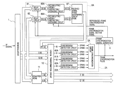
The absolute-phasing synchronization capturing circuit
- 25 -
CA 02293629 1999-12-08
according to the first embodiment of the invention has a
demodulation circuit 1, a.remapper 11 made of a ROM, a
logical transformation circuit 12, a frame synchronism
detection block 2A, a frame synchronization signal
generator 6, and a received signal phase detection block
8A. The frame synchronism detection block 2A has
synchronism detection circuits 40A to 43A and a frame
synchronization circuit 5A. The received signal phase
detection block 8A has delay circuits 81 and 82,
accumulating/adding/subtracting/averaging circuits 85A and
86A, and a received signal phase determining circuit 87.
Baseband signals I(8) and Q(8) demodulated by the
demodulation circuit 1 are supplied to the remapper 11
which rotates the baseband signals I(8) and Q(8) by a phase
of A = 45° and outputs baseband signals i(8) and q(8).
First, the remapper 11 will be described. The
remapper 11 is made of a ROM and rotates supplied baseband
signals I ( 8 ) and Q ( 8 ) by a phase of A - 45 ° and outputs
baseband signals i(8) and q(8).
Specifically, ~ - -45° is substituted into the
equations (2) and (3) to calculate the following equations
(4) and (5) which result in the following equations (6) and
26 -
CA 02293629 1999-12-08
(7):
i(8) - I cos(-45) - Q sin(-45) ...
(4)
q(8) - I sin(-45) + Q cos(-45) ...
(5)
i(g) _ I(1/~2) Q(-1/~2) - (1/,~2)(I +
- Q)
... (6)
q(8) - I(-1/,~2) + Q(1/,~2) - (1/~2) (-I + Q)
... (7)
In the remapper 11, the input baseband signals I ( 8 )
and Q(8) are remapped into baseband signals rotated by a
phase angle of 45° in the clockwise direction. This
remapper 11 does not require an input of the phase rotation
angle signal RT(3) so that the ROM memory capacity can be
reduced to 1/8 of the conventional remapper 7.
The phase rotation angle signal RT(3) output from the
received signal phase detection block 8A, the baseband
signals I(8) and Q(8) demodulated by the demodulation
circuit 1, and the baseband signals i(8) and q(8) remapped
by the remapper 11 are input to the logical transformation
circuit 12.
The logical transformation by the logical
transformation circuit 12 input with such signals will be
described. Figs. 2(a) and 2(b) and Fig. 3 show truth
- 27 -
CA 02293629 1999-12-08
tables illustrating the operation of the logical
transformation circuit 12.~ The truth table shown in Fig.
2(a) is used for n = even, i.e., for 8 = 45° x n (n = 0, 2,
4, 6), and the truth table shown in Fig. 2(b) is used for
n = odd, i.e., for A = 45° x n (n = 1, 3, 5, 7). The truth
table shown fn Fig. 2 shows BPSK demapping outputs for a =
45° x n (n = 0, 1, 2, 3, 4, 5, 6, 7) .
In accordance with the phase rotation angle signal
RT(3), the input baseband signals I(8) and Q(8) are
logically transformed into the absolute-phase baseband
signals I'(8) and Q'(8) by using the truth table shown in
Fig. 2(a) ff n = even. For example, if the phase rotation
angle signal RT(3) is "000", it means the reception at the
absolute phase. Therefore, the baseband signal I'(8) is
the baseband signal I(8), and the baseband signal Q'(8) is
the baseband signal Q(8). If the phase rotation angle
signal RT(3) is "010", ft means the phase rotation angle of
A = 90°. In this case, the equations (2) and (3) have been
used conventionally to convert as in the following
equations (8) and (9):
I'(8) - I cos(-90°) - Q sin(-90°) - Q(8)
... (8)
Q'(8) - I sin(-90°) + Q cos(-90°) - -I(8)
--- (9)
28 -
CA 02293629 1999-12-08
This conversion, however, can be realized simply by
inverting the sign of the baseband signal I(8) input to the
logical transformation circuit 12 and by replacing the
baseband signal Q(8) by the sign inverted baseband signal
I(8). Similarly, for the phase rotation angle signals
RT(3) - "100" and RT(3) - "110", the conversion can be
performed by using the truth table shown in Fig. 2(a).
In accordance with the phase rotation angle signal
RT(3), the input baseband signals i(8) and q(8) are
logically transformed into the absolute-phase baseband
signals I'(8) and Q'(8) by using the truth table shown in
Fig. 2(b) if n = odd. For example, if the phase rotation
angle signal RT ( 3 ) is "001" , it means the phase rotation
angle of 8 = 45°. Therefore, the baseband signal I'(8) is
the baseband signal i(8), and the baseband signal Q'(8) is
the baseband signal q(8). It is sufficient therefore if
the baseband signals i(8) and q(8) themselves output from
the remapper 11 are used as the baseband signals I'(8) and
Q'(8).
If the phase rotation angle signal RT(3) is "011", it
means the phase rotation angle of A =,135°. In this case,
the baseband signals i(8) and q(8) whose phases are rotated
by the phase rotation angle of 8 = 45°, are further rotated
- 29 -
CA 02293629 1999-12-08
by a phase rotation angle of 8 - 90°. Therefore, the
following equations (10) and (11) are calculated:
I' - i cos(-90°) - q sin(-90°) - q(8)
... (10)
Q' - i sin(-90°) + q cos(-90°) - -i(8)
... (11)
Therefore, this conversion can be realized simply by
inverting the sign of the baseband signal i(8) input to the
logical transformation circuit 12 and by replacing the
baseband signal q(8) by the sign inverted baseband signal
i(8). Similarly, for the phase rotation angle signals
RT(3) - "101" and RT(3) - "111", the conversion can be
performed by using the truth table shown in Fig. 2(b).
The logical transformation circuit 12 receives the
phase rotation angle signal RT(3) corresponding to the
phase rotation angle 8, baseband signals I(8) and Q(8), and
baseband signals f ( 8 ) and q ( 8 ) remapped by the remapper 11,
and performs the logical transformation by using the truth
table shown in Fig. 3 to output the BPSK demapped outputs
to the synchronism detection circuits 40A, 41A, 42A and
43A.
The operation of the logical transformation circuit 12
-
CA 02293629 1999-12-08
including the BPSK demapping will be specifically described
with reference to Fig. 4. Inverters 121 to 124 of the
logical transformation circuit 12 invert the signs of the
baseband signals I(8) and Q(8) and the baseband signals
I(8) and q(*) whose phases were rotated by the remapper 11
by the angle of 8 = 45°. A multiplexer 125 selects proper
baseband signals from the supplied baseband signals I(8),
Q(8), i(8) and q(8) and the supplied sign-inverted baseband
signals I(8), Q(8), i(8) and q(8), in accordance with the
phase rotation angle signal RT(3), and outputs the selected
baseband signals as output baseband signals I'(8) and
Q'(8). This selection of the output baseband signals I'(8)
and Q' ( 8 ) by the multiplexer 125 is performed in accordance
with the truth tables shown in Figs. 2(a) and 2(b).
Further, as indicated by solid lines in Fig. 4, of the
baseband signals input to the multiplexer 125, an MSB of
I(8) is extracted to use it as an output B0, an MSB of i(8)
is extracted to use it as an output B1, an MSB of Q(8) is
extracted to use it as an output B2, and an MSB of q(8) is
extracted to use it as an output B3, respectively to the
synchronism detection circuits 40A to 43A. A circuit
specialized to the BPSK demapping is therefore unnecessary
and the conventionally used BPSK demapper 3 is not
necessary. If a ROM is used for the table conversion by
- 31 -
CA 02293629 1999-12-08
the BPSK demapper 3, this ROM is not necessary and the
memory having a capacity of~ 216 x 8 bits can be omitted.
This can be clarified from the BPSK demapping
illustrated in Fig. 16. Namely, in Fig. 16(a), the
judgement result that the signal point of the baseband
signal is the bit "1" or "0" is equal to the I axes of the
signal point, i.e., the MSB of the baseband signal I(8).
The judgement result for A - 45° shown in Fig. 16(b) is
equal to the MSB of the baseband signal i(8) output from
the remapper 11. This is also applicable to the judgement
results for other phase rotation angles. From this reason,
the conventionally used BPSK demapper 3 can be omitted.
As indicated by broken lines in Fig. 4, of the
baseband signals input to the multiplexer 125, an MSB of an
inverted I(8) may be extracted to use it as an output B0,
an MSB of an inverted i(8) may be extracted to use it as an
output B1, an MSB of an inverted Q(8) may be extracted to
use it as an output B2, and an MSB of an inverted q(8) may
be extracted to use it as an output B3, respectively to the
synchronism detection circuits 40A to 43A.
This is apparent from the logical inversion relations
between the outputs for a - 0° and 8 - 180°, between the
L~
- 32 -
CA 02293629 1999-12-08
outputs for A - 45° and 8 - 225°, between the outputs for
a = 90° and A = 270°, and between the outputs for a =
135°
and a = 315°.
Next, the synchronism detection circuits 40A to 43A
will be described by taking as a representative example the
synchronism detection circuit 40A. Also for the
synchronism detection by the synchronism detection circuit,
the logical inversion relations are used between the
outputs for A = 0° and a = 180°, between the outputs for a
- 45° and 8 - 225°, between the outputs for A - 90° and A
- 270°, and between the outputs for a = 135° and A =
315°.
The synchronism detection circuit is configured so that it
can detect "SYNCPAT", "nSYNCPAT" and these logically
inverted bit streams.
Fig. 5 shows an embodiment of the synchronism
detection circuit 40A. The synchronism detection circuit
40A is constituted of: shift registers DO to D15; an AND
gate 55 input with outputs from the shift registers D15,
D10 and D8; an AND gate 55A input with inverted outputs
from the shift registers D15, D10 and D8; an AND gate 56
input with outputs from the shift registers D14 to D11 and
D9; an AND gate 56A input with inverted outputs from the
shift registers D14 to D11 and D9; an AND gate 57 input
- 33 -
CA 02293629 1999-12-08
with outputs from the shift registers D7, D6 and D3; an AND
gate 57A input with inverted outputs from the shift
registers D7, D6 and D3; an AND gate 58 input with outputs
from the shift registers D5, D4, and D2 to D0; and an AND
gate 58A input with inverted outputs from the shift
registers D5, D4, and D2 to D0.
The bit streams of the frame synchronization signals
capable of being captured by the synchronism detection
circuit 40A are "SYNCPAT" and "nSYNCPAT" as well as these
logically inverted bit streams of the frame synchronization
signals, i.e., (1, l, 1, 0, 1, 1, 0, 0, 1, 0, l, 0, 0, 0,
0, 1) and last half 8-bit inverted bit stream (l, 1, 1, 0,
1, 1, 0, 0, 0, 1, 0, 1, 1, 1, 1, 0) which are also written
as "SYNCNPAT" and "nSYNCNPAT" respectively.
The last half 8 bits of "SYNCPAT" are equal to the
last half 8 bits of "nSYNCNPAT", and the last half 8 bits
of "nSYNCPAT" are equal to the last half 8 bits of
"nSYNCNPAT". The frame synchronization signal is divided
into the first half 8 bits and the last half 8 bits. The
synchronism detection circuit 40A can capture the bit
streams of the frame synchronization signals of "SYNCPAT",
"nSYNCPAT", "SYNCNPAT" and "nSYNCNPAT", by performing AND
operations of the outputs RRLO, RFHO, FRHO and FFLO from
34 -
CA 02293629 1999-12-08
the AND gates 55 to 58 and the outputs of RRHO, RFLO, FRLO
and FFHO from the AND gates 55A to 58A, as shown in Fig. 6.
The logical operations shown in Fig. 6 are performed
in accordance with the AND operation outputs. Therefore,
the bit streams of the frame synchronization signals of
"SYNCPAT", "nSYNCPAT", "SYNCNPAT" and "nSYNCNPAT" can be
captured. Further, as shown in Fig. 7, the synchronization
detection output SYNAO can be obtained through the OR
operation of "SYNCPAT" and "SYNCNPAT", and the
synchronization detection output SYNBO can be obtained
through the OR operation of "nSYNCPAT" and "nSYNCNPAT".
The above description is also applicable to the
synchronism detection circuits 41A, 42A and 43A. The
outputs of the AND gates of the synchronism detection
circuits 41A, 42A and 43A are used as the outputs RRH1 to
RRH3, RFLl to RFL3, FRL1 to FRL3, and FFH1 to FFH3, and the
AND operations and OR operations shown in Figs. 6 and 7 are
performed. It is therefore possible to obtain the
synchronization detection outputs SYNA1, SYNBl, SYNA2,
SYNB2, SYNA3 and SYNB3.
As described above, the synchronism detection circuit
40A can provide the functions of both the conventional
- 35 -
CA 02293629 1999-12-08
synchronism detection circuits 40 and 44. Therefore, the
synchronism detection circuits 40A to 43A input with the
BPSK demapping outputs BO to B3 from the logical
transformation circuit 12 corresponding to the angles a of
0°, 45°, 90° and 135° can capture the frame
synchronization
signals corresponding to all the received signal phase
rotation angles.
The numbers of synchronism detection circuits and
shift registers are halved as compared to the conventional
circuit. The circuit scale can therefore be reduced.
The outputs of the synchronism detection circuits 40A
to 43A are supplied to the frame synchronization circuit 5A
having OR gates 61 and 62 shown in Fig. 8. If it is
confirmed that a OR output SYNA of SYNAa (a = 0 to 3) and
a OR output SYNB of SYNBa (a - 0 to 3) are alternately
received at a predetermined frame pitch, it is judged that
there is a frame synchronization and a frame
synchronization pulse is output at each frame period. This
operation is similar to the conventional circuit.
Next, the frame synchronization circuit 5A, frame
synchronization signal generator 6 and received signal
phase detection block 8A will be described. The
36 -
CA 02293629 1999-12-08
demodulated baseband signals I(8) and Q(8) are supplied to
the received signal phase detection block 8A to detect the
phase rotation angle signal RT(3).
Upon reception of the frame synchronization pulse
output from the frame synchronization circuit 5A, the frame
synchronization signal generator 6 supplies a reproduced
frame synchronization signal and a frame synchronization
signal section signal to the received signal phase
detection block 8A.
The symbol streams of the frame synchronization
signals in the demodulated baseband signals I(8) and Q(8)
are supplied via the delay circuits 81 and 82 to the
accumulating/adding/subtracting/averaging circuits 85A and
86A. In this case, the delay circuits 81 and 82 operate to
m a k a t h a i n p a t t i m i n g o f t h a
accumulating/adding/subtracting/averaging circuits 85A and
86A coincide with the input timing of the reproduced frame
synchronization signal output from the frame
synchronization signal generator 6. The input gates of the
accumulating/adding/subtracting/averaging circuits 85A and
86A are opened in response to the frame synchronization
signal section signal output from the frame synchronization
signal generator 6, so that the symbol streams DI ( 8 ) and
- 37 -
CA 02293629 1999-12-08
DQ(8) of the frame synchronization signals output from the
delay circuits 81 and. 82 are subjected to an
adding/subtracting process by the
accumulating/adding/subtracting/averaging circuits 85A and
86A.
For the adding/subtracting operation by the
accumulating/adding/subtracting/averaging circuits 85A and
86A, an adding operation is performed if the bit stream is
"1", whereas a subtracting operation is performed ff the
bit stream is "0". After the adding/subtracting operation
for a predetermined number of sections, an averaging
operation is performed to output averaged reception point
signals AVI(8) and AV(8) from the
accumulating/adding/subtracting/averaging circuits 85A and
86A.
The reception point signals AVI(8) and AV(8) output
from the accumulating/adding/subtracting/averaging circuits
85A and 86A are input to the received signal phase
determining circuit 87 made of a ROM. By referring to the
received signal phase determining table, the phase rotation
angle signal RT(3) of three bits corresponding to the
received signal phase rotation angle is output to the
logical transformation circuit 12. The logical
38 -
CA 02293629 1999-12-08
transformation circuit 12 received the phase rotation angle
signal RT(3) operates in the manner described already.
The received signal phase detection block 8A uses the
accumulating/adding/subtracting/averaging circuits 85A and
86A, in place of the 0°/180° phase rotation circuit 83 and
accumulating/adding/averaging circuits 85 and 86
respectively of the received signal phase detection block
8. The 180° phase rotation to be performed by the 0°/180°
phase rotation circuit 83 is equal to the sign inversion of
each axis. Therefore, the accumulating/adding operation
for the 180° phase rotated reception symbol at each axis is
equal to the accumulating/subtracting operation at each
axis. It is therefore possible to replace the 0°/180°
phase rotation circuit 83 and accumulating/adding/averaging
c i r c a i t s 8 5 a n d 8 6 b y t h a
accumulating/adding/subtracting/averaging circuits 85A and
86A. If the 0°/180° phase rotation circuit 83 is made of
a ROM, a memory capacity of 128 k bytes (= 216 x 16 bits)
can be reduced. The received signal phase detection block
8A may be used fn place of the received signal phase
detection block 8 of the conventional absolute-phasing
synchronization capturing circuit shown in Fig. 14. Also
in this case, if a ROM is used for the table conversion by
the 0°/180° phase rotation circuit 83, a memory capacity of
- 39 -
CA 02293629 1999-12-08
128 k bytes can be reduced.
In the absolute-phasing synchronization capturing
circuit of the first embodiment described above, although
the remapper 11 rotates the phases of the baseband signals
i(8) and q(8) by 8 - 45°, the remapper 11 may rotate the
phase by 8 - 135°, 225° or 315°.
In this case, in order to obtain the BPSK demapping
outputs, although the logical transformation circuit 12
performs the same logical transformation shown in Fig.
2(a), it performs a logical transformation shown in Fig.
9(a) in place of the logical transformation shown in Fig.
2(b) if the phase rotation by a - 135° among 8 - 45° x n
(1, 3, 5, 7) i.s to be performed. If the phase rotation by
a - 225° fs to be performed, the logical transformation
shown in Fig. 9(b) is performed, and if the phase rotation
by a = 315° is to be performed, the logical transformation
shown in Fig. 9(c) i.s performed. In addition, in place of
the logical transformation shown in Fig. 3, the logical
transformation shown in Fig. 10(a), 10(b) or 10(c)
corresponding to the logical transformation shown in Fig.
9(a), 9(b) or 9(c) is performed respectively.
The absolute-phasing synchronization capturing circuit
40 -
CA 02293629 1999-12-08
according to a second embodiment of the invention will be
described. Fig. 11 is a block diagram showing the
structure of the absolute-phasing synchronization capturing
circuit according to the second embodiment of the
invention.
In the absolute-phasing synchronization capturing
circuit according to the second embodiment of the
invention, a frame synchronization detection block 2' is
used in place of the frame synchronization detection block
2 of the conventional absolute-phasing synchronization
capturing circuit shown in Fig. 14. The other structures
are the same as those of the conventional absolute-phasing
synchronization capturing circuit.
The frame synchronization detection block 2' will be
described. As shown in Fig. 12, a BPSK demapper 3A
includes BPSK demappers 30, 31, 32 and 33 which output B0,
B1, B2 and B3, respectively. These outputs are supplied to
synchronism detection circuits 40A, 41A, 42A and 43A. The
synchronism detection circuits have the structure shown in
Fig. 5 and perform the logical operation shown in Figs. 6
and 7. Outputs SYNAO and SYNBO of the synchronism
detection circuit 40A, outputs SYNA1 and SYNB1 of the
synchronism detection circuit 41A, outputs SYNA2 and SYNB2
- 41 -
CA 02293629 1999-12-08
of the synchronism detection circuit 42A, and outputs SYNA3
and SYNB3 of the synchronism detection circuit 43A are
supplied to a frame synchronization detection circuit 5A
having the OR gate circuit shown in Fig. 8.
In the absolute-phasing synchronization capturing
circuit constructed as above according to the second
embodiment of the invention, the frame synchronization
detection block 2' receives the demodulated baseband
signals I(8) and Q(8), and the BPSK demapper 3A performs
BPSK demapping to obtain the outputs B0, B1, B2 and B3.
Similar to the absolute-phasing synchronization capturing
circuit according to the first embodiment of the invention,
the synchronism detection circuits 40A to 43A supply the
outputs SYNAa and SYNBa to the frame synchronization
circuit 5A which in turn outputs the frame synchronization
pulse.
According to the absolute-phasing synchronization
capturing circuit according to the second'embodiment of the
invention, the circuit scale of the BPSK demapper 3A is a
half of that of the BPSK demapper 3, the number of
synchronism detection circuits is only four including the
synchronism detection circuits 40A to 43A, and the circuit
scale of the synchronism detection circuits is halved as
42 -
CA 02293629 1999-12-08
compared to the conventional circuit.
Next, the absolute-phasing synchronization capturing
circuit according to a third embodiment of the invention
will be described. Fig. 13 is a block diagram showing the
structure of the absolute-phasing synchronization capturing
circuit according to the third embodiment of the invention.
In the absolute-phasing synchronization capturing
circuit according to the third embodiment of the invention,
a frame synchronization detection block 2A' is used in
place of the frame synchronization detection block 2A of
the absolute-phasing synchronization capturing circuit
according to the first embodiment of the invention. The
received signal phase detection block is the same as the
conventional circuit.
The frame synchronization detection block 2A' uses the
conventional synchronism detection circuits 40 to 47 in
place of the synchronism detection circuits 40A to 43A. An
MSB of an inverted I(8), an MSB of an inverted i(8), an MSB
of an inverted Q(8) and an MSB of an inverted q(8)
respectively indicated by broken lines in Fig. 6 are
further extracted from the logical transformation circuit
12 shown in Fig. 6 to use them as the outputs B4, B5, B6
- 43 -
CA 02293629 1999-12-08
and B7 which are supplied to the synchronism detection
circuits 40 to 47. Outputs SYNAO to SYNA7 and SYNBO to
SYNB7 from the synchronism detection circuits 40 to 47 are
supplied to the frame synchronization circuit 5.
The frame synchronization is detected in accordance
with the BPSK demapping outputs BO to B7 generated by the
logical transformation circuit 12A. The BPSK demapper 3
used conventionally is not necessary, and only the logical
transformation circuit 12A having a small and simple
circuit is used. The circuit scale of the absolute-phasing
synchronization capturing circuit can therefore be reduced.
As described so far, according to the absolute-phasing
synchronization capturing circuit of this invention, the
circuit scale can be reduced considerably, and the chip
area of an IC which fabricates the absolute-phasing
synchronization capturing circuit thereon can be used
efficiently.
- 44 -