Note: Descriptions are shown in the official language in which they were submitted.
CA 02293660 2003-09-30
- 1 -
HIGH EFFICIENCY CHANNEL DROP FILTER
WITH ABSORPTION INDUCED ON/OFF SWITCHING AND MODULATION
This invention was made with government support under
Grant No. 9400334-DMR awarded by National Science
Foundation. The government has certain rights in the
invention.
BACKGROUND OF THE INVENTION
The invention relates to channel drop filters, and in
particular to a highly efficient resonator-system channel
drop filter. In exemplary embodiments, photonic crystal
channel drop filters are provided.
The increasing interest in photonic integrated circuits
(PICs) and the increasing use of all-optical fiber networks
as backbones for global communication systems have been
based in large part on the extremely wide optical
transmission bandwidth provided by dielectric materials.
This has accordingly led to an increased demand for the
practical utilization of the full optical bandwidth
available. In order to increase the aggregate transmission
bandwidth, it is generally preferred that the spacing of
simultaneously transmitted optical data streams, or optical
data channels, be closely packed, to accommodate a larger
number of channels. In other words, the difference in
wavelength between two adjacent channels is preferably
minimized.
Channel dropping filters (CDFs) that access one channel
of a wavelength division multiplexed (WDM) signal, and do
not disturb the other channels, are essential components of
PICs and optical communication systems. Among various
devices introduced recently, resonant filters are attractive
candidates for channel dropping because they can potentially
be used to select a single channel with a very narrow
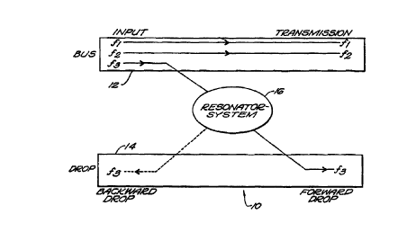
linewidth. A schematic block diagram of a resonator-system
CDF 10 is shown in FIG. 1, where two waveguides, the bus 12
and the drop 14, are coupled through a resonator-system 16
having one or more resonant cavities. The bus 12 includes
CA 02293660 1999-12-07
WO 98/57207 PCT/US98/11319
_ 2 _ _
an input port and an output port, and the drop 14 includes
a forward port and a backward port. While WDM signals (i.e.
multi-frequency signals) propagate inside one waveguide (the
bus), a single mode is transferred out of the bus and into
the other waveguide (the drop), either in the forward or
backward propagation direction, while completely prohibiting
cross talk between the bus and the drop for all other
frequencies.
It will be appreciated by those skilled in the art that
a channel drop filter, for the purposes of describing the
invention, is a filter that can transfer a channel from one
waveguide to another, such as dropping a channel from the
bus to the drop or adding a channel from the drop to the
bus.
The performance of a CDF is determined by the transfer
efficiency between the two waveguides. Perfect efficiency
corresponds to 100 transfer of the selected channel into
either the forward or backward direction in the drop, with
no transmission or back reflection into the bus. All other
channels should remain unaffected by the presence of the
optical resonator.
It is also desirable to obtain on/off switching
functionality in the CDF. In ether words, it is desirable
to be able to switch on and off the transfer of a frequency
channel. Ideally, in an "on" state, the frequency channel
is completely transferred from the bus to the drop
waveguide, while in an "off" state, the frequency channel
remains unperturbed in the bus waveguide. It is conceivable
to achieve such on/off functionality using frequency tuning
mechanisms. However, to turn off the device, the r -~nant
frequencies of the coupling element must be shifted _ of
the entire frequency range of the signal. Such a frequency
shift tends to require large switching power, and is not
very practical.
Accordingly, it is an object of the invention to use an
absorption-induced switching effect to achieve the desired
on-off functionality.
CA 02293660 2003-09-30
-3-
SUI~zARY OF THE INVENTION
A highly efficient channel drop filter employs a
coupling element including a resonator-system between two
waveguides, which contains at least two resonant modes. The
resonator-system may include one or more interacting resonant
cavities which in addition to being coupled to the
waveguides, can also be coupled directly among themselves and
indirectly among themselves via the waveguides. Each
component of the coupling element can be configured or
adjusted individually. The geometry and/or dielectric
constant/refractive index of the resonator-system can be
configured so that the frequencies and decay rates of the
resonant modes are made to be substantially the same in the
case where absorption is not induced inside the resonator-
system. The filter can achieve 100 signal transfer between
the waveguides at certain frequencies, while completely
prohibiting signal transfer at other frequencies. The filter
can be configured with photonic crystals.
The channel drop filter devices can have flat-top and
straight-sidewall lineshape characteristics. These lineshape
characteristics can be realized by using several resonances
to couple the waveguides, and by designing the relative
positioning of the frequency of each resonance with respect
to one another. The usage of multiple resonances also allows
the design of optical switches. These devices can switch the
signal from a forward to a backward direction, or from a
complete to a zero transfer.
The channel drop filter may have on/off switching
functionality. The switching can be achieved by incorporating
materials with tunable absorbing characteristics into the
coupling element. When the tunable material displays minimum
absorption, the frequency channel of interest is transferred
completely from the bus waveguide to the drop waveguide. When
the material displays maximum absorption, on the other hand,
the frequency channel is not transferred, but rather remains
CA 02293660 2003-09-30
-4-
undisturbed in the bus waveguide. The switching action can
be readily achieved with electrical or optical means.
According to one aspect of the invention there is
provided an electromagnetic field frequency filter which
S includes an input waveguide which carries a signal having at
least one frequency including at least one desired frequency,
and an output waveguide. A resonator-system is coupled to
the input and output waveguides which transfers the said at
least one desired frequency to the output waveguide and
allows transmission of undesired frequencies through the
input waveguide. The resonator-system comprises at least one
periodic dielectric structure and at least two resonators.
The resonator-system supports at least two system modes of
opposite symmetry with respect to the mirror plane, the
system modes consisting in part of a linear combination of
resonant modes of said resonators, at least two of the said
system modes having a frequency at or near the desired
frequency.
According to another aspect of the invention there is
provided an electromagnetic field frequency filter
comprising: an input waveguide which carries a signal having
at least one frequency including at least one desired
frequency; an output waveguide; and a resonator-system
coupled to said input and output waveguides operable for the
adjustable transfer of said at least one desired frequency to
said output waveguide and transmission of undesired
frequencies through said input waveguide in response to a
variation of the internal decaying rate or resonance
frequency of at least one resonator of said resonator-system,
said resonator-system being comprised of at least one
periodic dielectric structure, said resonator system further
being comprised of at least two resonators, said resonator-
system supporting at least two system modes of opposite
CA 02293660 2004-06-10
-4a-
symmetry, said system modes consisting in part of a linear
combination of resonant modes of said resonators, at least
two of said system modes having a frequency at or near said
desired frequency when said transfer occurs substantially.
According to another aspect of the invention there is
provided an electromagnetic field frequency filter
comprising: a waveguide having an input port and an output
port, said waveguide receiving a signal having at least one
frequency including at least one desired frequency; and a
resonator-system incorporated in said waveguide between said
input and output ports operable for the transmission of said
at least one desired frequency to said output port in
response to a variation of the internal decaying rate of at
least one resonator of said resonator-system, said resonator-
system defining at least one resonant mode, said variation of
the internal decaying rate is larger than the variation of
the resonance frequency.
According to another aspect of the invention there is
provided an electromagnetic field frequency filter
comprising: an input waveguide which carries a signal having
at least one frequency including at least one desired
frequency; an output waveguide; and a resonator-system
coupled to said input and output waveguides which transfers
said at least one desired frequency to said output waveguide
and allows adjustable transmission of undesired frequencies
through said input waveguide, said resonator-system being
comprised of at least two single-mode resonators, said
resonator-system supporting at least two system modes of
opposite symmetry, said system modes consisting in part of a
linear combination of resonant modes of said resonators, at
least two of said system modes having a frequency at or near
said desired frequency.
CA 02293660 2003-09-30
-4b-
According to another aspect of the invention there is
provided an electromagnetic field frequency filter
comprising: an input waveguide which carries a signal having
at least one frequency including at least one desired
frequency; an output waveguide; and a resonator-system
coupled to said input and output waveguides operable for the
adjustable transfer of said at least one desired frequency to
said output waveguide and transmission of undesired
frequencies through said input waveguide in response to a
variation of the internal decaying rate or resonance
frequency of at least one resonator of said resonator-system,
said resonator-system being comprised of at least two single-
mode resonators, said resonator-system supporting at least
two system modes of opposite symmetry, said system modes
consisting in part of a linear combination of resonant modes
of said resonators, at least two of said system modes having
a frequency at or near said desired frequency when said
transfer occurs substantially.
BRIEF DESCRIPTION OF THE DRAWINGS
FIG. 1 is a schematic block diagram of a generic
resonator-system CDF;
FIGs. 2A and 2B are schematic diagrams of contour plots
of the resonant mode field patterns in a CDF structure having
a mirror-plane symmetry perpendicular to the waveguides, and
a resonator-system supporting two resonant states by using
two interacting cavities each of which supports a monopole
mode, and by using one cavity which supports a doubly
degenerate hexapole mode, respectively;
FIG. 3 is a plan view diagram of an exemplary embodiment
of a resonator-system photonic crystal CDF in accordance with
the invention;
CA 02293660 2003-09-30
-4c-
FIG. 4 is a schematic diagram of the physics mechanism
for channel dropping in an exemplary filter having a
resonator-system supporting one even and one odd degenerate
mode;
FIG. 5 is a graph of the frequency spectrum of the even
CA 02293660 1999-12-07
WO 98/57207 PCT/US98/11319
- 5 -
and odd modes for the CDF of FIG. 3;
FIGs. 6A-6C are graphs of the spectrum of transmitted
signal, and the signal in the forward and backward drops,
respectively, for the CDF shown in FIG. 3;
FIG. 7 is a computed electric field pattern at the
resonant frequency of the CDF shown in FIG. 3;
FIG. 8 is a plan view diagram of an alternative
exemplary embodiment of a resonator-system photonic crystal
CDF in accordance with she invention;
FIG. 9 is a computed electric field pattern of the
modes of the resonator-system of the CDF shown in FIG. 8;
FIG. 10 is a plan view diagram of another alternative
exemplary embodiment of a resonator-system CDF in accordance
with the invention;
FIG. 11 is a schematic block diagram of a CDF in which
the coupling element is composed of external and internal
sub-elements;
FIG. I2 is a schematic block diagram of a resonator-
system CDF with two external sub-elements;
FIG. 13 is a plan view diagram of an exemplary
embodiment of a resonator-system photonic crystal CDF with
four point defects in accordance with the invention;
FIG. 14 is a graph of the frequency spectrum of the
even-even, odd-even and odd-odd modes for the CDF of FIG.
13;
FIGs. 15A-15C are graphs of the intensity spectrum of
a transmitted signal in the bus, the intensity spectrum of
a transmitted signal in the forward drop, and the intensity
spectrum of a transmitted signal in the backward drop,
respectively, of the CDF of FIG. 13;
FIG. 16 is a plan view diagram of an exemplary
embodiment of a resonator-system photonic crystal CDF with
two point defects aligned perpendicularly to the associated
waveguides;
FIG. 17 is a plan view diagram of an exemplary
embodiment of a resonator-system photonic crystal CDF with
two point defects having local symmetry but not global
symmetry;
CA 02293660 2003-09-30
- 6 -
FIG. 18 is a plan view diagram of an exemplary
embodiment of a resonator-system photonic crystal CDF with
two point defects aligned parallel to the associated
waveguides;
FIG. 19 is a plan view diagram of an exemplary
embodiment of a resonator-system photonic crystal CDF with
six point defects;
FIG. 20 is a plan view diagram of an exemplary
embodiment of a resonator-system photonic crystal CDF with
three cavities;
FIG. 21 is a plan view diagram of another alternative
exemplary embodiment of a resonator-system CDF utilizing
conventional channel waveguides with a photonic crystal
having four microcavities;
FIGS. 22A and 22B are functional block diagrams of a
channel drop filter utilizing the mechanism of
absorption-induced switching in the "on" state and "off"
state, respectively ;
FIGs. 23A and 23B are a plan view and a cross-sectional
view taken along line 23-23, respectively, of a photonic
crystal resonator-system switch/modulator CDF utilizing an
electrode to induce absorption;
FIGs. 24A and 24B are graphs showing the normalized
transmission and transferred spectra for the
switch/modulator shown in FIGS. 23A and 23B in an "on"
state;
FIGs. 25A and 25B are graphs showing the normalized
transmission and transferred spectra for the
switch/modulator structure shown in FIGs. 23A and 23B in an
"off" state;
FIG. 26 is a cross-sectional view of an exemplary
embodiment of a resonator-system switch/modulator CDF in
which absorption is induced through an optical fiber;
FIGS. 27A and 27B are a plan view and cross-sectional
view taken along line 27-27, respectively, of an exemplary
embodiment of a resonator-system switch/modulator CDF
utilizing electrodes to induce absorption;
FIG. 28 is a plan view of an exemplary embodiment of a
CA 02293660 1999-12-07
WO 98/57207 PCT/US98/11319
_ 7 - _
photonic crystal resonator-system switch/modulator CDF with
three cavities;
FIGS. 29A and 29B are a plan view and a cross-sectional
view taken along line 29-29, respectively, of an exemplary
embodiment of a waveguide switch/modulator;
FIGS. 30A and 30B are graphs showing the normalized
reflection and transmission spectra of the switch modulator
structure shown in FIGs. 29A and 29B in an "on" state; and
FIGS. 31A and 31B are graphs showing the normalized
reflection and transmission spectra of the switch modulator
structure shown in FIGS. 29A and 29B in an "off" state.
DETAILED DESCRIPTION OF T8E ILLUSTRATED EMBODIMENTS
The invention provides a design of a resonator-system
CDF (along with its basic properties) which achieves maximum
transfer efficiency. For purpose of clarity, the CDF of the
invention will be described with respect to embodiments
involving dropping a channel from the bus to the drop. It
will be appreciated by those skilled ir. the art that the CDF
of the invention can equally function to transfer a channel
from any one waveguide to another waveguide.
The design is based on a rigorous symmetry and
computational analysis. The CDF in accordance with the
invention uses a coupling element between two waveguides,
which has at least two resonant modes. The resonator-system
includes one or more interacting resonant cavities which in
addition to being coupled to the waveguides, can also be
coupled directly among themselves and indirectly among
themselves via the waveguides. Each component of the
coupling element can be configured or adjusted individually.
The geometry and/or dielectric constant/refractive index of
the resonator-system are configured so that the frequencies
and decay rates of the resonant modes are made to be
substantially the same. The aforementioned characteristic
is specific to the case where absorption is not induced
inside the resonator-system.
It will be shown that, in certain cases such as in the
case of a photonic crystal CDF, transfer efficiencies of
CA 02293660 2003-09-30
-
100 can be achieved. Two specific embodiments using
photonic crystals will be presented, as well as an
embodiment which is a combination of a photonic crystal
resonator-system and conventional waveguides. An embodiment
will also be presented which uses nonlinear materials to
achieve tuning of the CDF. In addition, further embodiments
of the invention will be described that utilize absorption
affects to induce on/off switching and modulation of the
CDF.
Initially, the generic CDF structure 10 shown in FIG.
1 must be considered to determine the basic properties
required to achieve 100$ transfer efficiency. At the
resonant frequency, the guided mode inside the bus waveguide
12 excites the modes of the resonator-system 16. In turn,
the resonator-system modes decay both into the bus waveguide
12 and into the drop waveguide 14.
The transmitted signal is composed of the input signal
and the signal which originates from the decay of the
resonator-system modes. By properly configuring the
resonator-system, it is possible for these signals to
interfere destructively and cancel each other, resulting in
zero transmission as required. The reflected signal, on the
other hand, originates entirely from the decay of the
resonator-system mode. To achieve perfect transfer
efficiency, the resonator-system is configured such that the
resonator-system signal does not decay into the backward
direction in the bus.
In order to achieve zero transmission and zero
reflection, it is necessary to have a structure with modes
of opposite symmetry. Consider the case in which the
structure of FIG. 1 has mirror-plane symmetry perpendicular
to the waveguides, and that the resonator-system supports
two resonant states, one with even symmetry, whose
electromagnetic field is labelled seven>, and one with odd
symmetry, whose electromagnetic field is labelled Todd>,
with respect to the mirror plane. Examples of even and odd
states are shown in FIGS. 2A and 2B, which are schematic
diagrams of contour plots of the resonant mode field
CA 02293660 1999-12-07
WO 98/57207 PCT/US98/11319
_ g _
patterns in a CDF structure having a mirror-plane symmetry
perpendicular to the waveguides, and a resonator-system
supporting two resonant states either by using two
interacting cavities each of which support a monopole mode,
or by using one cavity which supports a doubly degenerate
hexapole mode, respectively.
FIG. 2A shows the odd 200 and even 202 field patterns
of a structure with two coupled cavities supporting monopole
modes, and FIG. 2B shows the odd 204 and even 206 field
patterns of a structure with a single cavity supporting a
doubly-degenerate hexapole mode. The + and - signs indicate
the sign of the field. The two rectangles adjacent the
field patterns represent the bus 210 and drop 212
waveguides.
An incoming wave ei'°' can then be decomposed into the
form cos(kx) + isin(kx), where x corresponds to the
direction along the waveguides. The cos(kx) part, which is
even with respect to the mirror plane, couples only to the
even resonant state. The sin(kx) part, on the other hand,
is odd, and couples only to the odd resonant state. In the
specific case where the coupling constants are equal for
both modes, a resonant state of the form ~even> + i~odd~ is
excited, which in turn decays only along the forward
direction in the input waveguide. As a consequence,
reflection is completely absent.
Maximum CDF efficiency can be achieved, provided that
the following hold true. First, the structure possesses at
least one mirror plane perpendicular to the waveguides, and
supports at least two resonant.states of opposite symmetry.
Second, the two states have substantially the same
frequency. Third, the two states have substantially the
same quality factor, determined from the decay of the
resonances into the waveguide modes.
An exemplary embodiment of a resonator-system photonic
crystal CDF 300 in accordance with the invention is shown in
FIG. 3 in plan view. The CDF 300 includes a photonic
crystal 302 having two waveguides, a bus 304 and a drop 306.
The CDF also includes a resonator-system 307 which has two
CA 02293660 2003-09-30
- 10 -
point defects or cavities 308, 310. In contrast to other
types of resonant cavities, photonic crystal cavities can be
truly single mode as described in Villeneuve et al.,
"Microcavities in photonic crysta~s: Mode symmetry,
tunability, and coupling", Phys. Rev. B 54, 7837 (1996).
Furthermore, photonic crystal cavities do not suffer from
intrinsic radiation losses, and are somewhat insensitive to
fabrication-related disorder as described in Fan et al.,
"Theoretical investigation of fabrication-related disorder
on the properties of photonic crystals", Journal App. Phys.
78, 1415 (1995).
In the illustrated embodiment, the photonic crystal 302
is configured as a square lattice of high-index dielectric
posts 312 on a substrate such as silicon. The posts have a
radius of 0.20a and a dielectric constant of 11.56, where a
is the lattice constant. Two rows of posts are removed to
form the waveguides. The coupling element is introduced
between the waveguides by altering two posts, thereby
defining cavities 308, 310. Each of the cavities has a
radius of 0.05a and a dielectric constant of 6.6. The
cavities are five lattice constants apart and two lattice
constants away from the waveguide on each side. Each cavity
supports a localized monopole state which is singly
degenerate. The even and odd states are composed of linear
combinations of the two monopoles.
As will be appreciated by those of skill in the art,
such a CDF can be fabricated with a photonic crystal in
which the contrasting dielectric constants can be achieved
by creating channels or holes within a first dielectric
material and filling the channels or holes with air or a
second dielectric material having a different refractive
index than the first material. Examples of various photonic
crystal structures and methods of fabrication are found in
U.S. Pat. Nos. 5,187,461, 5,389,943, 5,440,421, 5,600,483,
5,784,400 and 5,682,401.
FIG. 4 is a schematic block diagram of the physics
CA 02293660 1999-12-07
WO 98/57207 PCT/US98/11319
- 11 -
mechanism used for channel dropping in accordance with the
invention for an exemplary filter having a resonator-system
405 supporting one even and one odd mode of substantially
the same frequency. The schematic includes a channel drop
filter 400 having a bus waveguide 402, a drop waveguide 404,
and the resonator-system 405 coupled therebetween. At the
resonant frequency, the guided mode inside the bus excites
both the even and odd modes. In turn, the even 406a-406d
and odd 407a-407d modes of the resonator-system decay
substantially equally both into the bus and into the drop.
The transmitted signal 408 is composed of three parts,
the input signal 410 and the signals 406b and 407b which
originate from the decay of the resonator-system modes.
These three parts interfere destructively, resulting in zero
transmission. The reflected signal 412, on the other hand,
is composed of two parts, signals 406a and 407a which
originate from the decay of the resonator-system modes.
Under the condition that the even and odd states have
substantially the same frequency and substantially the same
quality factor, as described heretofore, these two parts
cancel, resulting in zero reflection. In the exemplary
embodiment, there is no signal in either the backward or
forward direction in the drop. the choice of direction will
depend on the phase of the decaying amplitudes from the even
and odd modes into the bus and the drop.
The two cavities 308 and 310 of the CDF 300 shown in
FIG. 3 are coupled indirectly through the waveguides, and
directly through the crystal. Each coupling mechanism
splits the frequency (i.e. breaks the degeneracy) of the
even and odd states, but with an opposite sign. The exact
cancellation between the two coupling mechanisms is ensured
by changing the dielectric constant of four individual posts
314, 316, 318, 320 in the photonic crystal from 11.56 to
9.5. Alternatively, the radius or shape of the four
individual posts could be reduced in order to achieve the
same results.
Analytically, it can be shown that the quality factor
CA 02293660 2003-09-30
- 12 -
of the two states can be made equal provided that the
wavevector k of the guided mode satisfies the relation k~d
- nn+rr/2, where d is the distance between the two cavities
(defects), and n is an integer. This condition can be met
by separating the two cavities by f~.ve lattice constants,
and by choosing and altering the size and dielectric
constant of the defect posts in such away that the guided
mode at the resonant frequency has a wavevector of 0.25a'1.
To verify these assumptions, the filter response of the
exemplary structure shown in FIG. 3 is computed using a
finite-difference time-domain scheme. A pulse is sent down
one of the waveguides and excites both the even and odd
states. These two states then decay exponentially into the
waveguides. By Fourier transforming the decaying
amplitudes, the frequency spectrum of the even and odd modes
for the structure 300 can be found, each with a Lorentzian
lineshape, as shown in the graph of FIG. 5. The two line
shapes overlap almost completely, as desired.
The spectrum of the transmitted signal, and the signal
in the forward and backward drops are shown in the graphs of
FIGS. 6A-6C, respectively. The transmission efficiency is
close to 100 over the entire spectrum, except at the
resonant frequency, where it drops to 0~ as shown in FIG.
6A. The forward drop shows a Lorentzian lineshape with a
maximum close to 100 at resonance. The quality factor is
larger than 1000 as shown in FIG. 6B. The backward drop
shows almost complete absence of signal as shown in FIG. 6C.
FIG. 7 shows a computed electric field pattern at the
resonant frequency of the CDF 300 of FIG. 3. The electric
field exhibited is at maximum transfer efficiency at a
steady-state frequency of 0.3696c/a. The power is
completely transferred from the bus to the drop. The
simulation demonstrates the behavior of an ideal channel
drop filter.
FIG. 8 is an alternative exemplary embodiment of a
resonator-system photonic crystal CDF 800 in accordance with
the invention shown in plan view. The CDF 800 includes a
photonic crystal 702 having two waveguides, a bus 704 and a
CA 02293660 2003-09-30
- 13 -
drop 706. The photonic crystal 702 is configured as a
square lattice of high-index dielectric posts 708. The
posts have a radius of 0.20a and a dielectric constant of
11.56, where a is the lattice constant. Two rows of posts
are removed to form the waveguides. The coupling element
between the two waveguides is a resonator-system 709 which
consists of a single cavity 710 with two doubly-degenerate
modes (i.e. two modes with the same frequency). The cavity
is made by increasing the radius of a single post from 0.20a
to 0.60a. Alternatively, the cavity can be configured by
changing the dielectric constant of a single post. For the
illustrated embodiment, the dielectric constant would be
increased. Also, as described above, the photonic crystal
can be fabricated with channels or holes of air or material
having a contrasting dielectric constant.
FIG. 9 shows a computed electric field pattern of the
modes of the resonator-system of the CDF 800 shown in FIG.
8 without the presence of the waveguides. The field pattern
illustrates the two doubly-degenerate modes of the
resonator-system of the CDF 800 in the absence of the
waveguides. Since one of these modes is even and the other
odd, the exemplary structure resulting in the field pattern
shown in FIG. 9 satisfies the first and second conditions of
achieving maximum CDF efficiency, namely the structure
possesses at least one mirror plane, and supports at least
two resonant modes of opposite symmetry, and the two modes
have the same frequency. However, in the presence of
waveguides, the degeneracy is broken and the two modes
couple differently to the waveguides, hence they have
different quality factors. This will have the effect of
reducing the transfer efficiency below 100$. The transfer
efficiency can be optimized by chang.i.ng the shape of the
cavity, and/or by changing the size or the dielectric
constant of neighboring posts so that the resonant modes
have substantially the same frequency.
FIG. 10 is another exemplary embodiment of a resonator-
system CDF 900 in accordance with the invention. The CDF
900 includes two waveguides, a bus 902 and a drop 904. The
CA 02293660 2003-09-30
- 14 -
waveguides are conventional channel waveguides made of high
dielectric material on a substrate such as silicon. A
coupling element in the form of a resonator-system 906 is
configured from a photonic crystal including a dielectric
region 908 with a periodic series of holes 910. Within the
array of holes, two defects 912, 914 have been introduced by
breaking the periodicity. These two defects serve as
cavities. Alternatively, the holes can be replaced with
rods as described above.
The efficiencies of all the aforementioned exemplary
embodiments of the invention are optimized by configuring
and selecting parameters for the geometry and/or the
refractive index of the resonator-system. By choosing the
appropriate geometries and/or refractive indices for the
resonator-system, the frequencies of the degenerate modes
will be made to be substantially the same in accordance with
the criteria for efficiency. In addition, the geometry and
refractive index configuration of the resonator-system are
configured so that the decay or dissipation rates (quality
factors) of the degenerate modes are substantially the same
into the bus and drop waveguides.
Accordingly, the CDF 300 of FIG. 3 can be configured
such that the posts 314, 316, 318, and 320 are of varying
geometry, i.e., size and shape, with respect to the
remaining posts 312, rather than of varying dielectric
constant as described. Furthermore, the CDF 700 of FIG. 8
can be optimized by configuring the geometries and/or
refractive indices of the posts adjacent to the cavity 710.
For example, posts 712 and 714 can be configured to be of a
size smaller than the cavity 710, yet larger than the
remaining posts 708 in the photonic crystal. Alternatively,
the cavity can be configured by cutting or shaving the sides
of a single post to form a post with a diamond shape from
the top view. As an example of modifying the resonator-
system of CDF 900 of FIG. 10 so that the degenerate modes
and decay rates match, the dielectric region 908 can be
configured to be wider at regions adjacent the defects 912
and 914.
CA 02293660 2003-09-30
- 15 -
In a further exemplary embodiment, a design for a
tunable channel drop filter is considered. In every
embodiment described heretofore, the channel frequency was
determined by the geometry and dielectric constant of the
structure, which is fixed upon fabrication. In order to
dynamically change the frequency of the channel (i.e. in
order to drop a different frequency using the same device),
nonlinear materials can be used. The dielectric constants
of the resonator-system or of its surroundings can then be
configured using electronic, piezo-electric, thermal, or
electromagnetic mechanisms such as, but not limited, the
electro-optic effect, the charge-carrier effect, and the
photoionization of DX centers, allowing the CDF to be tuned.
An example of tuning the resonance of a resonator-system
using nonlinear materials is described by Villeneuve et al.,
"Single-mode waveguide microcavity for fast optical
switching", Optics Letters, Vol. 21, No. 24, 2017 (1996).
Channel dropping filters are important components of
photonic integrated circuits and optical communication
systems. These devices allow the access of one or several
frequency channels in a WDM signal, without disturbing the
other channels. Heretofore, devices have been presented
which employ at least two resonant modes as the coupling
element between two waveguides. Using two resonances
results in a Lorentzian-shaped transfer lineshape, or
response function. At the resonant frequency, the transfer
efficiency reaches 100%. As the frequency moves away from
the resonant frequency, the transfer efficiency decreases
rapidly. In a practical WDM system, there are uncertainties
in the resonant frequencies of the filters due to
fabrication-related disorders. Also signal frequencies
fluctuate due to temperature variations in the light
sources. A Lorentzian-shaped transfer function requires a
high degree of precision in filter fabrication and frequency
stability of the light source.
In contrast, a filter structure with a "flat-top"
response function can transfer signals of slightly different
CA 02293660 1999-12-07
WO 98/57207 PCT/US98/11319
- 16 -
frequencies with similar efficiencies, and thereby tolerate
a larger amount of structure and temperature variations.
Another practical consideration for filter designs concerns
the "sidewall" of the lineshape. A Lorentzian function
falls off as (bw)-2 far away from the resonant frequency,
where 6c~ is the difference between the signal frequency and
resonant frequency of the filter. In some practical
systems, faster fall-offs are required to reduce the cross
talk between nearby frequency channels.
To address these practical considerations, the
invention provides designs of channel drop filters with
customized response functions. These structures are
constructed by introducing several resonances, and by
appropriately adjusting the center frequency and the width
of these resonances. As exemplary embodiments, filter
structures transfer lineshapes are described which have both
the desired "flat top" and "sharp sidewall" characteristics.
In addition to its response lineshape, this design also
offers the possibility of unique switching functionality.
While this description__focus~es on filter structures which
have the "flat top" and sharp sidewall° response
characteristics, it will be appreciated by those skilled in
the art that other response functions can also be generated
using the structures described hereinafter.
In order to have transfer lineshape other then
Lorentzian, a structure is needed that supports more than
two resonances. FIG. 11 is a schematic block diagram of a
resonator-system CDF 1100 in accordance with the invention.
The CDF 1100 includes an input waveguide 1102, an output
waveguide 1104, and a resonator-system 1106 coupled between
the waveguides that supports several resonant modes. In
order for signal transfer to occur, it is necessary for the
resonator-system to consist of at least one external sub-
element, which couples directly into the input waveguide.
In the illustrated example, there is provided a bus external
sub-element 1108 and a drop external sub-element 1110. In
the specific case where only one external sub-element is
present, the sub-element should couple into both waveguides.
CA 02293660 1999-12-07
WO 98/57207 PCT/US98/11319
- 17 - _
The resonator-system can also contain internal sub-
elements 1112 that do not couple directly into the
waveguides, but rather only couple with other resonances.
Introducing internal sub-elements allows for greater
flexibility in designing filters with arbitrary response
lineshapes.
Each sub-element supports one or several local resonant
modes. A local resonant mode is an eigenmode of the sub-
element under the condition that the sub-element is isolated
from other parts of the system. Therefore, a local mode is
spatially associated with the sub-element. When
interactions are present, the local modes are not
necessarily eigenmodes of the entire system. Thus, in a CDF
structure, the local modes contain either one or several
frequency components. The actual positioning of these
frequency components is dependent on the nature of the
interactions between the sub-elements. Each sub-element can
also have a local symmetry, which is defined as the symmetry
that is only associated with the sub-element. The local
symmetry need not be identical to the symmetry of the
overall structure, referred to hereinafter as the global
symmetry .
It is necessary for the external sub-element that
couples with the bus waveguide (referred to hereinafter as
the bus sub-element) to possess a local mirror-plane
symmetry perpendicular to the waveguides, and to support at
least two local modes with opposite symmetries, i.e., there
should be at least one even and at least one odd local
modes. In order to achieve zero reflection, the decaying
amplitude of these modes into the backward direction should
add up to zero. In the case where only two local modes are
present, it is necessary for one to be even, while the other
one odd, with respect to the mirror plane. To achieve
cancellation of the decaying amplitudes in the backward
direction of the bus waveguide, the lineshape of these two
modes must overlap substantially, which in turn requires the
corresponding components in these two modes to have
substantially the same center frequency and the same width.
CA 02293660 1999-12-07
WO 98/57207 PCT/US98/11319
- 18 -
In the case where more than two local modes are present, it
is only necessary for the sum of the decaying amplitudes
from all the even modes to cancel the sum of that from all
the odd modes.
From energy conservation consideration it follows that,
to achieve complete transfer, it is necessary for the energy
in the resonator-system to decay into the bus waveguide and
the drop waveguide at the same rate. This can be achieved,
for example, by having a structure with a mirror plane
parallel to the waveguides. To achieve unidirectional
transfer into either the forward or the backward direction
of the drop waveguide, the external sub-element that couples
with the drop waveguide (referred to hereinafter as the drop
sub-element) should also have the properties of possessing
a local mirror plane and supporting local modes with
opposite symmetry.
The transfer lineshape can be customized by adjusting
the interaction between the sub-elements, and by adjusting
the interaction between the resonator-system and the
waveguides. The number of channels that get dropped depends
on the frequency spacing between the different channels, and
on the width of the CDF transfer function. It may be
desirable, in some cases, to increase the width of the
transfer function to allow the transfer of more frequency
channels. This can be accomplished, for example, by
increasing the number of local resonant modes in the
resonator system.
To summarize, an embodiment of the invention provides
an electromagnetic field frequency filter comprising an
input waveguide which carries a signal having a plural=~-y of
modes including a desired guided mode and an output
waveguide. A resonator-systEsn is coupled between the input
and output waveguides which transfers the desired guided
mode to the output waveguide and allows transmission of the
remaining frequencies through the input waveguides. The
resonator-system contains an external sub-element that
couples with the input waveguides. The external sub-element
possesses a local mirror plane perpendicular to the
CA 02293660 1999-12-07
WO 98/57207 PCT/US98/11319
- 19 -
waveguides, and defines at least two local resonant modes of
opposite symmetry with respect to the mirror plane. The
resonant modes have components which cancel in the backward
direction of the input waveguide, resulting in no
reflection.
As an example, consider a structure that can generate
a maximum-flat line-shape transfer function. An example of
a maximum-flat transfer function T (c~) is defined as:
4
( 0)4 Y4 . (1)
where c.~o is the center frequency and Y is the half width at
half maximum. Such a transfer function has both the desired
"flat top" and "sharp-sidewall" characteristics. To satisfy
the requirements described heretofore, consider a structure
that possesses two mirror planes, one parallel and the other
one perpendicular to the waveguide as in FIG. 12.
FIG. 12 is a schematic block diagram of a resonator-
system CDF 1200. The CDF 1200 has an input waveguide 1202,
an output waveguide 1204, and a resonator-system 1206
consisting of two external sub-elements 1208, 1210, and no
internal sub-element. Each of the external sub-elements is
made up of two cavities (not shown) adjacent to a waveguide
and supports two local resonant modes. The sub-element
1208, which couples with the input waveguide 1202, supports
an even local mode labelled ~l,e), and an odd local mode
labelled ~l,o). The even and odd properties are defined
with respect to the mirror plane perpendicular to the
waveguides, which in this example is also the local mirror
plane of the sub-elements.
Due to the interaction between the two sub-elements,
these local modes are not eigenstates of the overall
structure. The four eigenstates of the structure possess
different symmetry properties with respect to the two mirror
planes and are labelled according to their symmetry
CA 02293660 2003-09-30
-~ 2 0 -
properties. The state even-odd), for example, is even with
respect to the mirror plane parallel to waveguide, and odd
with respect to the mirror plane perpendicular to the
waveguide. Each eigenstate has a Lorentzian lineshape, and
is characterized by its center frequency and width.
The local modes can be expanded in terms of the
eigenstate of the system. In the case of sub-element 1208,
for example,
1, e) _ ~ ( ~ a ven - a ven) + ~ odd - a ven) )
1, o) _ ~ ( ~ even - odd )+ ~ odd - odd ) ) . ( 3 )
From such an expansion, it will be understood that the
lineshape of each local mode is made up of a sum of two
Lorentzian functions. In order to achieve zero reflection,
these two lineshapes must cancel. Cancellation can be
achieved in one of two ways:
Possibility 1:
seven-even - W odd-even - ~''~ 1 ~
seven-odd - Todd-odd - ~2
Yeven-even Yodd-even Yeven-odd - Yodd-odd - Y i ( 6 )
Possibility 2:
seven-even Todd-odd ' ~1 ~ (7)
CA 02293660 1999-12-07
WO 98/57207 PCT/US98/11319
- 21 -
seven-odd Todd-even - ~2
Yeven-even Yodd-even Yeven-odd Yodd-odd - Y ~ ( 9 )
where each c~ is the center frequency for the corresponding
eigenmode, and each y is the width. In the first scenario,
the wave is transferred along the forward direction of the
drop waveguide, while in the second scenario the wave is
transferred along the backward direction of the drop
waveguide.
To achieve a maximum-flat transfer lineshape in both
scenarios, the coupling strength between the two sub
elements is adjusted. Such coupling has the effect of
splitting the even and odd eigenmodes with respect to the
mirror plane parallel to the waveguides. In the case where
the frequency splitting is substantially equal to twice of
the width of the eigenstates, i.e.,
~1W2=2Y. (10)
the structure displays a maximum-flat transfer function.
In addition, the transfer can be entirely eliminated by
imposing all four states to have the same frequency and the
same width, i.e.,
seven-even - Todd-even - seven-odd Todd-odd ( 11 )
Yeven-even Yodd-even Yeven-odd Yodd-odd ( 12 )
In order to "switch" the transfer from the forward
direction to the backward direction, or to eliminate the
CA 02293660 1999-12-07
WO 98/57207 PCT/US98/11319
- 22 -
transfer, one needs to shift the resonant frequency on the
order of one width of a resonance peak, which can be as
small as one-thousandth of the center frequency. such a
frequency shift is readily achievable using non-linear
effects such as, but not limited to, the Kerr effect in
semiconductor materials.
FIG. 13 is a plan view diagram of another exemplary
embodiment of a resonator-system photonic crystal CDF 1300.
The CDF 1300 includes a photonic crystal 1301 having two
waveguides, a bus 1302 and a drop 1304. The photonic
crystal 1301 is configured as a square lattice of high-index
dielectric posts 1318. The posts have a radius of 0.20a and
a dielectric constant of 11.56, where a is the lattice
constant. Two rows of posts are removed to form the
waveguides.
The coupling element between the two waveguides is a
resonator-system 1303 which consists of four point defects
defining microcavities 1306,1308,1310,1312. The
microcavities are made, for example, by decreasing the
radius of the four posts from 0.20a. Alternatively, the
cavity can be configured by changing the dielectric constant
of the four posts. Also, as described above, the photonic
crystal can be fabricated with channels or holes of air or
material having a contrasting dielectric constant.
The microcavities are grouped into two external sub-
elements, a bus sub-element 1314 and a drop sub-element
1316. These sub-elements possess a local mirror plane
symmetry perpendicular to the waveguides which, in the
illustrated embodiment, is also the mirror plane of the
overall structure. There is no internal sub-element in this
geometry. The cavities are five lattice constants apart and
two lattice constants away from one of the c.-~veguides. Each
cavity supports a localized monopole state which is singly
degenerate. The even and odd states, as described, are
composed of linear combinations of these monopoles.
The quality factor of these symmetric states can be
made equal provided that the wavevector k of the guided mode
satisfies the relation k~d=nrr+rrl2, where d is the distance
CA 02293660 1999-12-07
WO 98/57207 PCT/US98/11319
- 23 -
between the defect in the direction parallel to the
waveguides, and n is an integer. This condition can be met
by separating the defects by five lattice constants, and by
choosing the size and dielectric constant of the defect
posts in such a way that the guided mode at the resonant
frequency has a wavevector of 0.25a-1.
The monopoles are coupled indirectly through the
waveguides, and directly through the photonic crystal along
the x-direction. Each coupling mechanism splits the
frequencies (i.e. breaks the degeneracy) of states of
different symmetries with respect to the mirror plane
perpendicular to the waveguide, but with an opposite sign.
The exact cancellation between the two coupling mechanisms
is ensured by changing the dielectric constant, size and/or
shape of selected rods, such as posts 1320,1322,1324,1326,
in the photonic crystal from 11.56 to 7.5, as shown in FIG.
13. The distance between the cavities in the y-direction is
chosen to be four lattice constant to ensure the appropriate
splitting in frequency between the states with opposite
symmetries with respect to the mirror plane parallel to the
waveguides.
The filter response of the structure shown in FIG. 13
can be computed using a finite-difference time-domain
scheme. A pulse is sent down one of the waveguides and
excites the resonant states. These resonant states then
decay exponentially into the waveguides. By Fourier
transforming the decaying amplitudes, the frequency spectrum
of all the symmetric states can be found, each with a
Lorentzian lineshape. FIG. 14 is a graph of the frequency
spectrum of the even-even, odd-even and odd-odd modes for
the CDF 1300 of FIG. 13. As required, the lineshapes of the
even-even 1400 and odd-even 1402 states overlap almost
completely, as well as the lineshapes of the even-odd 1404
and odd-odd 1406 states. The center frequency of the even-
even state is separated with the center frequency of the
even-odd state by twice the width of the resonant peak, as
desired.
The spectrum of the signal in the forward and backward
CA 02293660 1999-12-07
WO 98/57207 PCT/US98/11319
- 24 -
drops are shown in FIGs. 15A-15C along with the spectrum of
the transmitted signal. FIGs. 15A-15C are graphs of the
intensity spectrum of a transmitted signal in the bus, the
intensity spectrum of a transmitted signal in the forward
drop, and the intensity spectrum of a transmitted signal in
the backward drop, respectively, of the CDF 1300 of FIG. 13.
The transmission is close to 100 over the entire spectrum,
except in the neighborhood of the center frequency, where it
drops to 0~ (FIG 15A). The forward drop reaches a maximum
close to 99$ at the center frequency (FIG. 15B). The
backward drop shows almost complete absence of signal (FIG.
15C). The transfer lineshape does indeed show the maximum-
flat characteristics, i.e., flattening of the top at the
resonance peak and sharp fall-off of the transfer amplitude
away from the center frequency.
FIG. 16 is a plan view diagram of another exemplary
embodiment of a resonator-system photonic crystal CDF 1600.
The CDF 1600 is configured from a photonic crystal 1601 of
a square lattice of high-index dielectric posts 1603, with
a bus waveguide 1602 and a drop waveguide 1604. In this
embodiment, the coupling element between the two waveguides
is a resonator-system 1605 which consists of two point
defects defining two cavities 1606,1608, each supporting
doubly degenerate modes (i.e. two modes with the same
frequency). The respective centers of the point defects are
aligned to an axis that is perpendicular to the waveguides.
Each of the cavities defines an external sub-element, a bus
sub-element 1610 and a drop sub-element 1612. There is no
internal sub-element in this structure.
The cavities 1606,1608 are made by increasing the
radius of two rods from 0.20a to 0.60a. The symmetric modes
arE composed of linear combinations of all .tee modes. The
frequencies of the symmetric modes can be tuned by changing
the shape and dielectric constant of the defect rods, and/or
the rods that are in the nearest neighbor position to the
defects. In addition, the splitting of frequencies between
modes with different symmetries with respect to the mirror
plane parallel to the waveguides can be adjusted by changing
CA 02293660 1999-12-07
WO 98/57207 PCT/US98/11319
- 25 - _
the distance between the defects, and by changing the shape
or dielectric constants of the rods lying between the
cavities. Using these tuning mechanisms, the resonant
frequencies can be placed at approximate positions to
achieve a complete transfer into the forward direction with
a maximum flat transfer lineshape.
FIG. 17 is a plan view diagram of another exemplary
embodiment of a resonator-system photonic crystal CDF 1700.
The CDF 1700 is configured from a photonic crystal 1701 of
a square lattice of high-index dielectric posts 1703, with
a bus waveguide 1702 and a drop waveguide 1704. In this
embodiment, the coupling element between the two waveguides
is a resonator-system 1705 which consists of two point
defects defining two cavities 1706,1708.
The CDF 1700 contains two external sub-elements. Each
of the cavities defines an external sub-element, a bus sub-
element 1710 and a drop sub-element 1712. There is no
internal sub-element in this structure. Each of these sub-
elements possesses a local mirror plane, and consists of a
single defect that supports two local resonances with
opposite symmetries with respect to the local mirror plane.
In contrast to the previous embodiments, there is no global
mirror plane in the structure. In order to achieve complete
transfer, the lineshapes of the even and the odd local modes
need to be cancelled. This can be achieved, for example, by
changing the dielectric constant or the size of the posts
adjacent to the cavities. By adjusting the dielectric
constant or the~size of the rods lying between the cavities,
the coupling between the local resonances in the two
cavities can be adjusted.
FIG. 18 is a plan view diagram of another exemplary
embodiment of a resonator-system photonic crystal CDF 1800.
The CDF 1800 is configured from a photonic crystal 1801 of
a square lattice of high-index dielectric posts 1803, with
a bus waveguide 1802 and a drop waveguide 1804. In this
embodiment, the coupling element between the two waveguides
is a resonator-system 1805 which consists of two point
defects defining two cavities 1806, 1808, each supporting two
CA 02293660 1999-12-07
WO 98/57207 PCT/US98/11319
- 26 - _
doubly degenerate modes (i.e. two modes with the same
frequency). The respective centers of the point defects are
aligned along an axis that is parallel to the waveguides .
Each of the cavities defines a single external sub-element
1810. There is no internal sub-element in this structure.
The geometry of CDF 1800 introduces an indirect
coupling pathway between the cavities, which could be used
to tune the resonant frequencies of the symmetric modes, in
addition to the other mechanisms present in the previous
embodiments. With this additional mechanism, a complete
transfer into either the forward or the backward direction
can be achieved. Also the transfer can be eliminated
completely.
FIG. 19 is a plan view diagram of another exemplary
embodiment of a resonator-system photonic crystal CDF 1900.
The CDF 1900 is configured from a photonic crystal 1901 of
a square lattice of high-index dielectric posts 1903, with
a bus waveguide 1902 and a drop waveguide 1904. In this
embodiment, the coupling element between the two waveguides
is a resonator-system 1905 which consists of six point
defects defining six cavities 1906,1908,1910,1912,1914,1916,
each of which supports a singly degenerate resonance.
The CDF 1900 contains two external sub-elements. The
cavities 1906 and 1908 define an external bus sub-element
1918, and the cavities 1914 and 1916 define an external drop
sub-element 1920 a bus sub-element 1910 and a drop sub-
element 1912. The two cavities 1910,1912 in the center do
not couple directly to the waveguides, but rather only
couple to the waveguides through other cavities. This
structure is an example of a CDF with an internal sub-
~:lement 1922. In this case, the Fresence of the internal
sub-element does not affect the overlap of the even and odd
local states of the external sub-elements, but rather only
changes the frequencies of the even and odd states. By
adjusting the distance between the cavities and the
dielectric constants of the rods lying between the cavities,
more complex lineshapes such as the Butterworth function can
be achieved. In addition, the exact cancellation between
CA 02293660 1999-12-07
WO 98/57207 PCT/US98/11319
- 27 -
the coupling mechanisms is ensured by changing the
dielectric constant, size and/or shape of selected rods,
such as posts 1924,1926,1928,1930 in the photonic crystal.
FIG. 20 is a plan view diagram of another exemplary
embodiment of a resonator-system photonic crystal CDF 2000.
The CDF 2000 is configured from a photonic crystal 2001 of
a square lattice of high-index dielectric posts 2003, with
a bus waveguide 2002 and a drop waveguide 2004. In this
embodiment, the coupling element between the two waveguides
is a resonator-system 2005 which consists of three point
defects defining three cavities 2006,2008,2010. The
respective centers of the point defects are aligned along an
axis that is parallel to the waveguides. The cavities
define a single external sub-element 2012. There is no
internal sub-element in this structure.
In contrast to the previously illustrated embodiments,
the external sub-element 2012 of this structure contains
three local resonances, one odd, the other two even, with
respect to the mirror plane perpendicular to the waveguides.
Since there is only one external sub-element and no internal
sub-element, these local modes are eigenstates of the entire
filter structure. Complete transfer can occur if the
lineshape function of the odd mode cancels the sum of the
lineshape of the two even modes. This can be achieved by
having the center frequency of the odd modes lying between
the center frequencies of the two even modes, and by having
the width of the odd modes larger than the width of the two
even modes. The relative position of the frequencies of the
even and odd modes can be adjusted by changing the
dielectric constant or the size of the center cavity, since
the even modes have a large amplitude while the odd mode has
a small amplitude in the center cavity. The width of these
modes can be adjusted by changing the distance between the
cavities. The exact cancellation in the coupling mechanism
is ensured by changing the dielectric constant, size and/or
shape of selected rods, such as posts
2014,2016,2018,2020,2022,2024, in the photonic crystal.
Preferably, the posts 2016 and 2022 will be altered in a
CA 02293660 1999-12-07
WO 98/57207 PCT/US98/11319
- 28 - _
manner different than the alteration of the remaining posts
2014,2018,2020,2024.
FIG. 21 is a plan view diagram of another alternative
exemplary embodiment of a resonator-system CDF 2100. The
CDF 2100 utilizes conventional channel bus 2102 and drop
2104 waveguides made of high dielectric material with a
resonator-system 2105 configured from a photonic crystal.
The CDF 2100 is a case with radiation losses.
The resonator-system 2105 is made of two dielectric
regions 2106,2108, each consisting of a periodic series of
holes 2110. For each region, within the array of holes, two
defects 2112,2114/2116,2118 have been introduced by breaking
the periodicity. These defects act like microcavities. In
contrast to the two previously illustrated embodiments,
where there were no radiation losses, the two defect states
decay into both radiation modes and waveguide modes. The
condition for achieving maximum transfer to the forward
direction with the maximum-flat lineshape, in the presence
of radiation loss, therefore becomes:
seven-even Todd-even seven (13)
seven-odd Todd-odd Todd ( 14 )
Yeven-even Yodd-even Yeven-odd Yodd-odd Y ( 15 )
Yeven-even - Yodd-even - Yeven-odd - Yodd-oad - Y* ( 16 )
_
seven Todd 2 Y ( 17 )
CA 02293660 1999-12-07
WO 98/57207 PCT/US98/11319
- 29 -
where each w is the center frequency for the corresponding
eigenmode, each Y is the width of the resonance peak, and
each Y* is the width of the resonance peak due only to the
energy dissipation into the waveguides.
It will be appreciated by those skilled in the art that
the number of channels that get dropped depends on the
frequency spacing between the different channels, and on the
width of the CDF transfer function. It may be desirable, in
some cases, to increase the width of the transfer function
to allow the transfer of more frequency channels. This can
be accomplished, for example, by increasing the number of
local resonant modes in the resonator system.
Highly efficient channel drop filter structures have
now been presented. These structures allow the complete
transfer of one or several frequency channels in a
wavelength division multiplexed (WDM) signal from the bus
waveguide through a coupling element to the drop waveguide,
without disturbing the other channels. Tuning mechanisms
have also been introduced to shift the resonant frequencies
of the coupling element, which allows dynamic selection of
frequency channels. In addition to such channel-selection
capability, however, it is also preferable in a practical
WDM system to be able to switch on and off the transfer of
a frequency channel. Ideally, in an "on" state, the
frequency channels) is completely transferred from the bus
to the drop waveguide, while in an "off" state, the
frequency channels) remains unperturbed in the bus
waveguide. It is conceivable to achieve such on/off
functionality using the frequency tuning mechanism presented
heretofore. However, to turn off the device, the resonant
frequencies of the coupling element must be shifted out of
the entire frequency range of the WDM signal. Such a
frequency shift tends to require large switching power, and
is not very practical.
In accordance with further embodiments of the
invention, there now will be described the use of an
absorption-induced switching effect to achieve the on-off
functionality. The basic operating principle of this effect
CA 02293660 1999-12-07
WO 98/57207 PCT/US98/11319
- 30 -
is illustrated in FIGs. 22A and 22B. FIGs. 22A and 22B are
functional block diagrams of a channel drop filter 2200
utilizing the mechanism of absorption-induced switching in
the "on" state and "off" state, respectively. The filter
2200 includes a bus waveguide 2202, a drop waveguide 2204
and a resonator system 2206 which serves as the coupling
element as previously described. A material with a tunable
absorbing coefficient is incorporated in the coupling
element. Depending on the value of the absorption
coefficient, the filter is switched between an "on" state as
shown in FIG. 22A and an "off" state as shown in FIG. 22B.
In an "on" state, the material has a minimal absorption
coefficient and the structure behaves as a regular channel
drop filter, as described previously. At the resonant
frequency, the power is completely transferred from the bus
waveguide to the drop waveguide. The transmitted amplitude
in the bus waveguide drops to zero due to destructive
interference between the decaying amplitudes from the
coupling element and the incoming wave. The power is
transferred into the drop waveguide through the decaying
amplitude from the coupling element. For illustrative
purposes, FIG. 22A shows transfer along the backward
direction in the drop waveguide. The same applies equally
to the case where the power is transferred along the forward
direction.
In an "off" state, the absorbing material in the cavity
is tuned to have maximum absorption coefficient.
Consequently, the resonances in the coupling element are
spoiled and the decaying amplitudes from the coupling
element are eliminated. It is no longer necessary for the
frequencies and decay rates of the resonant modes to be
substantially the san:. ~ . In the drop waveguide, since the
wave power originates entirely from the decaying amplitudes,
the power transfer is completely turned off. In the bus
waveguide, on the other hand, with the absence of the
decaying amplitude, there is no longer destructive
interference. Hence, the transmission of the incoming wave
will stay close to 100 over the entire frequency range as
CA 02293660 1999-12-07
WO 98/57207 PCT/US98/11319
- 31 -
shown in FIG. 22B.
It will be appreciated that in both the "off" and "on"
states, there is minimal signal loss due to absorption. In
the "on" state, the absorption coefficient is minimized, and
by design there should be minimal losses associated with
absorption. In such a state, photons possess a large field
amplitude inside the coupling element. In the "off" state,
on the other hand, by introducing a large absorption
coefficient, the resonances in the coupling elements are
spoiled. The photons no longer possess a large field
amplitude in the coupling element. The only absorption loss
is due to the tunneling effect through the exponential tail
of the waveguide mode. Such a t.unnelir_g effect is minimized
by increasing the distance, and hence the tunneling barrier,
between the waveguide and the coupling element.
Quantitatively, the response spectra of the switch is
determined by the internal decaying rate vin and the external
decaying rate veX of the resonances. The internal decaying
rate is associated with cavity loss. When cavity loss is
induced by material absorption, the internal decaying rate
is defined by:
v1°=cx' ~ (18)
n
where a is the absorption coefficient of the materials, c is
the speed of light in vacuum, and n is the index of
refraction. The external rate, on the other hand, is
defined by the rate at which photons tunnel into the
waveguide and escape from the resonator system.
The decaying rates are related to the internal and
external quality factors through the relations:
Qzn - n ~ (19)
CA 02293660 1999-12-07
WO 98/57207 PCT/US98/11319
- 32 -
Qex =
Vexi (20)
where c~ is the resonant frequency. The quality factors Qin
and Qe" measure the number of optical cycles photons spend
in the resonator before being absorbed or leaking out,
respectively.
A detailed quantitative analysis can be constructed by
identifying the properties of the states of each individual
component, i.e., the propagating state in the waveguides,
and the resonant states in the coupling element. A
Hamiltonian matrix is then set up to describe the
interactions between these states. The transfer
characteristics can be extracted from such a Hamiltonian
matrix using a Green function's approach. As an example, in
the specific case where only a single pair of states is
present in the coupling element, and where the states
possess opposite symmetry with respect to the mirror plane
parallel to the waveguides, the following transfer spectra
exist (the subscripts a and o label the even and odd
states, respectively):
Transmission coefficient:
z
1 lVex 1 lVox
Z'bus- 1- - (21)
2 ~ (~-~3e+lVex+lVen 2 ~ CJ-~'uo-ElVox+lVon
Reflection coefficient:
1 lVex 1 lVox
Rb~s - + - ' (22 )
2 ~ CJ-~Te+lVex+lVen 2 G7-L5o+lVox+lVon
Transfer coefficient in the forward direction:
CA 02293660 1999-12-07
WO 98/57207 PCT/US98/11319
- 33 -
z
ex ex
1 1ve 1 1v° (23)
Tfdro
2 ~ CJ-~e+lVex+lVen 2 ~ (~-~3°+lVox+lVon
Transfer coefficient in the backward direction:
Z
ex ex
1 ive + 1 , ivo (24)
Tbdro
2 ~ CJ W3e +IVex +lVen 2 W-~5a +IVox +lVon
Of particular interest are two limiting cases. In one
llmlt, Vin is much less than vex, ( vin « Vex } ~ 1 . a . , the
absorption coefficient of the tunable material in the
coupling element is small. ven and von can then be ignored
in equations (21}-(24). The equations, therefore, describe
a channel drop filter response without material absorption.
At the resonant frequency, all the power is transferred from
the bus waveguide to the drop waveguide. The switch is in
an "on" state. In the opposing limit, vin is much less than
vex, ( vin » vex ) , i . a . , the absorption coef f icient of the
tunable material in the coupling element is large. From
equation (21), the transmission coefficient approaches
unity, while the reflection and the transfer coefficients
in equations (22)-(24) asymptotically vanishes with
increasing ven and von . Hence, the switch is in an "off"
state. The frequency channel of interest remains
propagating unperturbed in the bus waveguide. The analytic
results indeed confirm the qualitative arguments presented
earlier.
Equivalently, due to the relation between the decaying
rates and the quality factors (equations (19) and (20)),
the two limiting cases can be presented in terms of the
internal and external quality factors. The "on" state
corresponds to the case when gin ~ Qex, while the "of f " state
corresponds to the case when Qin ~ Qex.
In general, the coupling element might support more
CA 02293660 2003-09-30
- 34 -
than two states. Also, the symmetries of these states
might be different from those specified above. In these
cases, the response spectra will be different from the
spectra given by equations (21)-(24). However, the general
feature of switching and modulation remains valid.
Introduction of absorption in a resonant cavity spoils the
resonant states) associated with the cavity and prevents
the cavity from contributing to the response of the filter
structure.
The absorption coefficients can be changed by different
means, whether electrical, optical or mechanical. For
example, see Soref et al., "Electrooptical Effects in
Silicon", IEEE J. Quantum Electron., QE-23, 123 (1987) and
Bennett et al., "Carrier-Induced Change in Refractive Index
of InP, GaAs, and InGaAsP", IEEE J. Quantum Electron.,
QE-26, 113 (1987).
The possibility of using the free carrier absorption effect
in semiconductor materials for electromagnetic waves with
frequencies lying below the electronic bandgap is presented.
When no optical or electrical excitations are present,
the conduction band is empty and the material is
transparent, i.e., the absorption coefficient is equal to
zero. Electrons can be injected into the conduction band of
the semiconductors with either optical excitations at a
frequency above the electronic band gap, or electronic
excitations such as current injection. Both excitations
have the effect of inducing free carrier absorption. In a
bulk silicon material, at a wavelength of 1.55 micron, the
absorption coefficient can be readily tuned from zero to
105m-1, which corresponds to a change of internal quality
factor from infinity to approximately 100. Significant
switching action can therefore be achieved in structures
with an external quality factor on the order of a thousand
or above. It is also noted that as the external quality
factor of the resonances increases, the magnitude of the
tuning range required for the absorption coefficients
decreases.
CA 02293660 1999-12-07
WO 98/57207 PCT/US98/11319
- 35 - _
While all of the previous descriptions have focused on
the switching aspect of the device, it will be appreciated
to people skilled in the art that a modulator functionality
can be achieved using the same device by modulating the
absorption coefficients with time. Optical modulators are
devices which perform the task of impressing information
onto a lightwave signal. As seen from equations (21)-(25),
the fraction of power switched between the waveguides
depends on the internal quality factor of the resonances,
which in turn is determined by the strength of material
absorption inside the cavity. For the case of no
absorption, the power is completed transferred to the drop
waveguide. For sufficiently large absorption, the power
remains unperturbed in the bus waveguide and no transfer
occurs. For intermediate values of absorption, power is
partially transferred to the drop waveguide. Thus, the
level of optical intensity in both the bus and the drop
waveguides can be modulated by the degree of material
absorption inside the cavities.
The general principle for switching and modulation
outlined above can be implemented in every embodiment
described herein. Rather than discussing the implementation
of the on/off functionality in all of the previous
embodiments, exemplary embodiments are presented to
illustrate the important practical issues.
As a first embodiment, the switching/modulation
functionality is incorporated on the photonic crystal
channel drop filter structure as shown in FIG. 8. The
channel drop filter structure includes a photonic crystal
having two waveguides, each formed by removing a row of
posts in a photonic crystal. The coupling element between
the two waveguides is a resonator-system which
consists of a single cavity. The geometrical parameters of
the structure have been previously specified. To
incorporate the switching/modulation functionalities,
materials are introduced into the resonant cavity which have
tunable absorbing characteristics.
FIGS. 23A and 23B are a plan view and a cross-sectional
CA 02293660 1999-12-07
WO 98/57207 PCT/US98/11319
- 36 -
view taken along line 23-23, respectively, of a photonic
crystal resonator-system switch/modulator CDF 2300 in
accordance with the invention. The CDF 2300 includes a
photonic crystal 2302 having two waveguides, a bus 2304 and
a drop 2306. The photonic crystal 2302 is configured as a
square lattice of high-index dielectric posts 2308. The
posts can have a radius of 0.20a and a dielectric constant
of 11.56, where a is the lattice constant. Two rows of
posts are removed to form the waveguides. The coupling
element between the two waveguides is a resonator-system
which consists of a single cavity 2310. The cavity is made
by increasing the radius of a single post from 0.20a to
0.60a. A buffer layer 2312 and an electrode 2314 are
attached to the cavity 2310 to transmit an electrical
excitation in the form of voltage or current.
Alternatively, as described above, the photonic crystal can
be fabricated with channels or holes of air or material
having a contrasting dielectric constant.
When the electrical excitation is not applied, the
material inside the cavity is transparent, (i.e. the
absorption coefficient is negligible), and a frequency
channel of interest is transferred from the bus waveguide to
the drop waveguide. Using a finite-difference time-domain
program as described previously, the transfer spectra is
computed, as shown in FIGS. 24A and 24B. FIGs. 24A and 24B
show the normalized transmission and transferred
spectra for the switch/modulator structure shown in FIGs.
23A and 23B. On resonance, a frequency channel is
completely transferred from the bus waveguide to the drop
waveguide in the backward direction. This condition is
referred to as the "on" state. In the simulation, the
external quality factor of the resonances is determined to
be close to 6,000.
When the electrical excitation is applied, on the other
hand, the material inside the cavity bscomes absorbing. It
has been shown that an internal quality factor of 100 is
achievable using readily available materials, such as Si, at
a wavelength of 1.55um. Both the external and internal
CA 02293660 1999-12-07
WO 98/57207 PCT/US98/11319
- 37 -
quality factors are related to the decaying rates via
equations (19) and (20). The response spectra are
determined using equations (21)-(25) and plotted in FIGs.
25A and 25B. FIGs. 25A and 25B show the normalized
transmission and transferred spectra for the
switch/modulator structure shown in FIGs. 23A and 23B. It
is noted that the transmission coefficient is close to 100
over the entire frequency range. The transfer from the bus
waveguide to the drop waveguide is therefore turned off.
This condition is referred to as the "off" state.
In another exemplary embodiment illustrated in FIG. 26,
a resonator-system switch/modulator CDF 2600, similar in
structure to CDF 2300, has absorption induced optically.
Instead of attaching electrodes to the surface of the
coupling element cavity 2602, an optical fiber tip 2604 is
used to deliver optical excitation locally into the coupling
element to change its absorbing characteristics. The
optical excitation is applied at a frequency above the
electronic bandgap of the semiconductors, which has the
effect of exciting electrons from the valence band to the
conduction band and to induce free electron absorption.
When such optical excitation is not applied, the material
inside the cavity remains transparent and the structure is
in an "on" state. When such optical excitation is applied,
on the other hand, the material inside the cavity becomes
absorbing and the structure is switched to an "off" state.
Instead of inducing absorption optically by using an
optical fiber tip, the switching can also be achieved
mechanically. The same structure as shown in FIG. 26 can be
used. In this case, however, there is no need to use
absorbing material in the cavities. When the fiber tip is
brought close to the cavity, the photon amplitude inside the
cavity can escape through the fiber tip. This is analogous
to the case where the material absorption is present. The
filter is in an "off" state. When the fiber tip is moved
away from the cavity, on the other hand, photons cannot
escape through the fiber tip. This is analogous to the
CA 02293660 1999-12-07
WO 98/57207 PCT/US98/11319
- 38 - _
previous case where the material absorption is absent. The
filter is in an "on" state.
In another exemplary embodiment of the invention, a
tunable absorbing material is introduced in the coupling
element of a channel drop filter structure similar to the
one shown in FIG. 21. FIGs. 27A and 27B are a plan view and
cross-sectional view taken along line 27-27, respectively,
of a resonator-system switch/modulator CDF 2700. The CDF
2700 utilizes conventional channel bus 2702 and drop 2704
waveguides made of high dielectric material with a
resonator-system 2705. In this embodiment, cavities 2710-
2716 are made by introducing defects in periodic surface
corrugations 2717,2718 on two waveguides 2706,2708 which
define the resonator-system located between the bus and the
drop. The waveguides 2706 and 2708 include a guiding layer
2720 and a cladding layer 2722. Furthermore, electrodes
2724 and 2726 are positioned above the cavities 2710 and
2712, respectively.
In contrast with the two previous embodiments, the
coupling element in the CDF 2700 is made of four cavities.
Two of the cavities (2710 and 2712) are adjacent to the bus
waveguide, while the other two cavities (2714 and 2716) are
adjacent to the drop waveguide. In this specific
embodiment, a separate electrode is attached to each cavity.
Since the electrical excitations applied to each electrode
can be varied independently, such configuration allows the
individual control over the absorbing characteristics of
each cavity, and therefore enables more complex switching
functionalities, as will be discussed hereinafter.
When electrical excitation is absent in all four
electrodes, the material inside the cavity is transparent
and a frequency channel is transferred from the bus
waveguide to the drop waveguide, as described previously.
Again, this condition corresponds to the "on" state. The
transfer can be completely turned off by applying electrical
excitations simultaneously on all the electrodes.
Alternatively, the transfer can also be turned off by
applying electrical excitations on only two of the cavities:
CA 02293660 1999-12-07
WO 98/57207 PCTNS98/11319
- 39 - -
either cavities 2710 and 2712, or cavities 2714 and 2716.
In addition to the functionality as an on/off switch
for transfer from one waveguide to the other, such structure
can be also dynamically configured as a narrow-band
reflector. Such functionality is achieved by applying
electrical excitations to three cavities: cavities 2714 and
2716, and either one of the cavities 2710 and 2712. In this
example, the excitation is applied on cavities 2710, 2712
and 2716. At resonance, the wave propagating in the bus
waveguide couples into cavity 2714, which in turn decays
only into the bus waveguide along both directions. The
incoming wave cancels the decaying amplitude along the
forward direction in the bus waveguide, leaving the wave to
be reflected into the backward direction. Since the
resonance displays a narrow-banded Lorentzian lineshape, the
reflection will occur only within a narrow frequency range,
and therefore the structure can be switched to perform the
functionality of a narrow band reflector.
In another exemplary embodiment of the invention, a
structure is considered that can switch the transfer from
the forward direction to the backward direction in the drop
waveguide, in addition to turning on and off the transfer.
FIG. 28 is a plan view diagram of a photonic crystal
resonator-system switch/modulator CDF 2800 in accordance
with the invention. The CDF 2800 includes a photonic
crystal 2802 with a periodic arrangement of elements such as
rods 2804, a bus 2806 and a drop 2808. The CDF 2800 can be
thought of as a combination of the channel drop filter
structures shown in FIGs. 3 and 8.
The coupling element is composed of three cavities: a
first cavity 2810, which is made of a rod with the radius
larger than all other rods and supports two resonant states
with opposite symmetry; and cavities 2812 and 2814, each
consisting of a rod with a radius smaller than other rods
and supporting a single resonant state. An electrode is
attached to each cavity, allowing electrical excitation to
be applied. In the case where the electrical excitation is
applied to all three cavities, the transfer between the bus
CA 02293660 2003-09-30
- 40 -
and drop waveguides is completely turned off. In the case
where the electrical excitation is applied only on the first
cavity 2810, the material inside the first cavity 2810
becomes absorbing while the material inside cavities 2812
and 2814 remains transparent. Consequently, the optical
signal is transferred through cavities 2812 and 2814 along
the forward direction in the drop waveguide.
When the electrical excitation is applied only to
cavities 2812 and 2814, on the other hand, the material
inside the cavities 2812 and 2814 become absorbing, while
the material inside cavity 2810 remains transparent.
Consequently, the signal is transferred through cavity 2810
along the backward direction of the drop waveguide. Hence,
by choosing the electrical excitations, one can switch the
device on and off, and one can also switch the device in
order for the optical signal to be transferred along either
the forward or the backward direction in the drop waveguide.
It will be appreciated by those skilled in the art that
the aforementioned embodiments work in a similar fashion
when it comes to adding a channel to a data stream. In the
absence of absorption, a frequency channel can be
transferred into the bus waveguide and added to the data
stream. In the presence of absorption, on the other hand,
such transfer is turned off. Absorption-induced
switching and modulation can further be achieved in the
structure of FIGS. 29A and 29B. FIGS. 29A and 29B are a
plan view and a cross-sectional view taken along line 29-29,
respectively, of a waveguide switch/modulator 2900. A
waveguide 2901 includes a periodic series of elements 2902
such as holes. A resonant microcavity 2904 is introduced
inside the waveguide by breaking the periodicity of elements
2902. The internal quality factor of the cavity can be
affected by different means, whether electrical, optical or
mechanical. In this specific embodiment, the internal
quality factor is affected by electrical means. Inside the
microcavity an absorbing material is introduced. An
electrode 2906, and a buffer layer 2908, is attached to the
cavity such that its absorbing characteristics can be
CA 02293660 2003-09-30
- 41 -
altered by electrical excitations.
For the case where the electrical excitation is absent,
the material inside the cavity is transparent. Away from
the resonant frequency, the signal is reflected by the
periodic array of holes. At the resonant frequency, on the
other hand, the incoming wave couples into the resonance.
The reflected signal, therefore, is composed of two parts,
a direct reflection from the holes, and the decaying
amplitude from the resonance along the backward direction of
the waveguide. These two parts cancel, leaving the signal
to be transmitted. The results of a finite difference time
domain simulation of such a microcavity structure are shown
in the graphs of FIGS. 30A and 30B. FIGs. 30A and 30B show
the normalized reflection and transmission spectra of the
switch/modulator structure shown in FIGS. 29A and 29B in an
"on" state. The transmission spectrum displays a Lorentzian
lineshape with a quality factor of 1500.
When the electrical excitation is applied, on the other
hand, the resonance inside the cavity is spoiled. In the
case where the internal quality factor is close to 100, the
response spectra is calculated using the Hamiltonian
approach described above and shown in FIGS. 31A and 31B.
FIGS. 31A and 31B show the normalized reflection and
transmission spectra of the switch modulator structure shown
in FIGS. 29A and 29B in an "off" state. The transmission is
almost completely turned off while most of the signal is
reflected. This device therefore allows us to switch
between transmission and reflection.
The foregoing description has been set forth to
illustrate the invention and is not intended to be limiting.
Since modifications of the described embodiments
incorporating the spirit and substance of the invention may
occur to persons skilled in the art.