Note: Descriptions are shown in the official language in which they were submitted.
CA 02293803 1999-12-08
WO 98/57381 PCTNS98/09563
ULTRA-'x'HIN LAYER ALKALINE EARTH METALS AS
STABLE ELECTRON-INJECTING CATHODES FOR
)POLYMER LIGHT EMITTING DIODES
RELATED APPLICATION
This application claims priority to U.S. Provisional Patent Application No.
08/872,657 filed 10 Junie 1997, the disclosure of which is incorporated herein
by reference.
TECHNICAL FIELD
This invention pertains generally to the field of light-emitting diodes
(LEDs).
More particularly, this invention relates to polymer LEDs which offer high
brightness,
high efficiency and extended operating life, and which comprise (a) a
transparent
hole-injecting anode layer; (b) an emissive layer comprising an
electroluminescent
polymer; and, (c) an electron-injecting cathode layer; wherein said cathode
layer comprises
an ultra-thin layer of allkaline earth metal (such as calcium, strontium and
barium) having a
thickness of about 100 ~ or less, typically from about 1 S to about 100 ~.
BACKGROUND
Throughout this application, various publications, patents, and published
patent
applications are referred to by an identifying citation; full citations for
these documents
may be found at the end of the specification immediately preceding the claims.
The
disclosures of the publications, patents, and published patent specifications
referenced in
this application are hereby incorporated by reference into the present
disclosure to more
fully describe the state of the art to which this invention pertains.
Diodes and particularly light-emitting diodes (LEDs) fabricated with
conjugated
organic polymer layers have attracted attention due to their potential for use
in display
technology. See, for e~4ample, Burroughs et al., 1990 and Braun et al., 1991.
Among the
CA 02293803 1999-12-08
WO 98/57381 PCT/US98/09563
2
promising materials for use as active layers in polymer LEDs are
poly(phenylene
vinylene), PPV, and soluble derivatives of PPV such as poiy(2-methyoxy-5-(2'-
ethyl-
hexyloxy)-1,4-phenylene vinylene), MEH-PPV, a semiconducting polymer with an
energy
gap Es of ~ 2.1 eV. This material is described in more detail in Wudl et al.,
1993. Another
material described as useful in active layers of polymer LEDs is poly(2,5-
bis(cholestanoxy)-1,4-phenylene vinylene), BCHA-PPV, a semiconducting polymer
with
an energy gap Es of ~ 2.2 eV. This material is described in more detail in
Zhang et al.,
1993. Other suitable polymers include, for example, the poly(3-
alkylthiophenes) (see, for
example, Braun et al., 1992) and related derivatives (see, for example,
Berggren et al.,
1995); polyp-phenylene) (see, for example, Grem et al., 1992), and its soluble
derivatives
(see, for example, Yang et al., 1993); and polyquinoIine (see, for example,
Parker et al.,
1994a). Blends of conjugated semiconducting polymers in non-conjugated host
polymers
are also useful as the active layers in polymer LEDs (see, for example, Zhang
et al., 1994).
Also useful are blends comprising two or more conjugated polymers (see, for
example, Yu,
1996). Generally, materials for use as active layers in polymer LEDs include
semiconducting conjugated polymers, more specifically semiconducting
conjugated
polymers which exhibit photoluminescence, and still more specifically
semiconducting
conjugated polymers which exhibit photoluminescence and which are soluble and
processible from solution into uniform thin films.
In the field of organic polymer-based LEDs it has been taught in the art to
employ a
relatively high work function metal as the anode, this high work function
anode serving to
inject holes into the otherwise filled ~-band ofthe semiconducting,
luminescent polymer.
Relatively low work function metals are preferred as the cathode material,
this low work
function cathode serving to inject electrons into the otherwise empty ~t*-band
of the
semiconducting, luminescent polymer. The holes injected at the anode and the
electrons
injected at the cathode recombine radiatively within the active layer and
light is emitted.
The common criteria for suitable electrodes are described in detail by Parker
et al., 1994b.
Suitable relatively high work function metals for use as anode materials are
transparent conducting thin films of indium/tin-oxide (see, for example,
Burroughs et al.,
1990; Braun et al., 1991 ). Alternatively; thin films of polyaniline in the
conducting
CA 02293803 1999-12-08
WO 98/57381 PCT/US98/09563
3
emeraldine salt form can be used (see, for example, Gustafsson et al., 1992;
Yang et al.,
1994; Yang, 1995; and Yang et al., 1995). Thin films of indium/tin-oxide and
thin films
of polyaniline in the ccbnducting emeraldine salt form are preferred because,
as transparent
- electrodes, both enable the emitted light from the LED to radiate from the
device in useful
levels.
Suitable relatively low work function metals for use as cathode materials
include
calcium, magnesium, and lithium. The thickness of the electron injection
cathode layer
has typically ranged from 200 to 5000 A (see, for example, Vanslyke, 1992;
Friend et al.,
1993; Nakano et al., 1994; and Kido et al., 1995). A lower limit of 200 to 500
~ is
required in order to fouln a continuous film (full coverage) for the cathode
layer (see, for
example, Holmes et al:, 1996; Scott et al., 1996; and Parker et al., 1994). In
addition to
good coverage, thicker cathode layers were believed to provide self
encapsulation to keep
oxygen and water vappr away from the active parts of the device.
Alloying of reactive cathode metals with more stable metals, such as aluminum
or
silver, has been used irl attempts to improve the cathode's environmental
stability;
however, the resulting; cathodes remain unstable to reaction with oxygen
and/or water
vapor (see, for example, Vanslyke, 1991; Vanslyke et al., 1991; and Heeger et
al., 1995).
Among the alkaline earth metals, calcium has been widely used in polymer LEDs.
Calcium is known to iiunction as an excellent electron-injecting contact.
Although
strontium and barium have work functions similar to that of calcium, there are
no reports
in the scientific literature concerning the use of either strontium or barium
as cathode
materials for polymer LEDs. This is probably due to the higher chemical
reactivity of
strontium and barium in comparison with calcium. Even calcium is highly
reactive, for
example, with oxygen; and water vapor at room temperature and even more
vigorously at
elevated temperatures, Consequently, either relatively thick films (> 1000 t~)
have been
used to provide some degree of self encapsulation or alloys with stable
metals, such as
aluminum, have been used as cathodes for LEDs, but with only limited success.
CA 02293803 1999-12-08
WO 98/57381 PCTNS98/09563
4
Despite in the improvements in the construction of polymer LEDs, a persistent
problem has been rapid decay of the device efficiency (and light output)
during stress,
especially at elevated temperature. Thus, there is a need for low work
function cathodes
for use as electron-injecting contacts in polymer LEDs, which have improved
stability to
reaction with oxygen and water vapor especially at elevated temperature.
The inventor has discovered the surprising and unexpected result that a
cathode
comprising an ultra-thin layer of an alkaline earth metal offers significant
improvements in
stability (e.g., extended stress lifetime) as compared to conventional
cathodes fabricated
from the same metals (and other low work function metals) but with films of
thickness
greater than 200 ~ (typically in the range 200 A to 5000 ~), the latter being
known in the
art.
Thus, the present invention pertains generally to cathodes comprising an ultra-
thin
layer (typically about 15 A to about 100 ~) of an alkaline earth metal (e.g.,
calcium,
strontium and barium), which functions as a stable contact for e~ciently
injecting
electrons into an emissive layer comprising an electroluminescent polymer,
thus resulting
in LEDs with high brightness, high efficiency and extended operating life.
SUMMARY OF THE INVENTION
The present invention pertains to polymer light-emitting diodes (LEDs) which
have
extended operating life, and more particularly, LEDs in which the decay of
efficiency and
light output is substantially postponed.
Thus, one aspect of the present invention pertains to a polymer light-emitting
diode
(LED) comprising:
(a) a transparent hole-injecting anode layer;
{b) an emissive layer comprising an electroluminescent polymer; and
(c) an electron-injecting cathode layer;
wherein said cathode layer comprises an ultra-thin layer of alkaline earth
metal
having a thickness of from about 15 to about 100 ~.
CA 02293803 1999-12-08
WO 98/57381 PCT/US98/09563
In one embodirtnent, the alkaline earth metal is selected from the group
consisting
of calcium, strontium, and barium.
5 In another embodiment, the ultra-thin layer of alkaline earth metal has a
thickness
of from about 30 to ab4ut 60 fir.
In another embpdiment, the cathode layer further comprises a capping layer. In
one
embodiment, the capping layer comprises aluminum, silver, or copper.
In another embpdiment, the electroluminescent polymer is a conjugated polymer.
In one embodiment, the electroluminescent polymer is selected from the group
consisting
of: polyp-phenylene vinylene)s, poly(arylene vinylene)s, polyp-phenylene)s,
poly(arylene)s, and povyquinolines. In one embodiment, the electroluminescent
polymer is
poly(2-(3,7-dimethyloCtyloxy)-S-methoxy-1,4-phenylene-1,4-phenylene vinylene).
In another embodiment, the anode layer comprises a material selected from the
group consisting of metal, metal oxide, graphite, doped inorganic
semiconductor, doped
conjugated polymer. Its one embodiment, the anode layer comprises a material
selected
from the group consisting of aluminum, silver, platinum, gold, palladium,
tungsten,
indium, copper, iron, l~ickel, zinc, lead, tin oxide, indium/tin oxide,
graphite; doped silicon,
doped germanium, doped gallium arsenide, doped polyaniline, doped polypyrrole,
and
doped polythiophene.
In another embodiment, the LED is encapsulated.
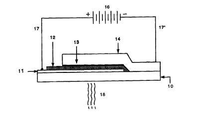
$RIEF DESCRIPTION OF THE DRAWINGS
Fig. 1 is a cross-sectional view of typical solid state LED device of the
invention
(not to scale). 10: substrate; 11: anode; i2: luminescent polymer; 13: ultra-
thin layer of
alkaline earth metal; l~: capping metal; 16 power source.
_. _._..~,u....~...... . ~.~..,...,~~....~.,w~..-~.._. .
CA 02293803 1999-12-08
WO 98/57381 PCT/US98/09563
6
Fig. 2 is a graph of luminance versus time for LED devices with different
thickness
of a calcium layer during continuous stress at 85°C and 8.3 mA/cmz.
Fig. 3 is a graph of luminance versus time for LED devices with different
thickness
of a barium layer during continuous stress at 85°C and 8.3 mA/cmz.
Fig. 4 is a graph of luminance versus time for LED devices with 40 t~ and 3000
~
layers of strontium, respectively, as a cathode layer, during continuous
stress at 85°C and
8.3 mA/cm2.
Fig. 5 is a graph of voltage at 25 mA versus time (indicating the voltage
increase
rate) for LED devices with 40 ~ layers of calcium, strontium, and barium
respectively, as a
cathode layer during continuous stress at 85°C and 8.3 mA/cmz. The
voltage increase rate
is indicated in parenthesis.
Fig. 6. is a graph of luminance versus time for comparative LED devices having
2000 ~ layers of a calcium/aluminum alloy as a cathode layer, during
continuous stress at
85°C and 8.3 mA/cmz.
DETAILED DESCRIPTION OF THE INVENTION
In one embodiment, the present invention pertains to a polymer light-emitting
diode (LED) comprising:
{a) a transparent hole-injecting anode layer;
(b) an emissive layer comprising an electroluminescent polymer; and
(c) an electron-injecting cathode layer;
wherein said cathode layer comprises an ultra-thin layer of alkaline earth
metal
having a thickness of from about 15 to about 100 ~.
A typical example of an LED of the present invention is illustrated in Figure
1,
wherein the cathode is fabricated from an ultra-thin layer of an alkaline
earth metal (layer
13 in Fig. 1 ). In other respects, the LEDs of the present invention are
similar to those
known in the art. That is, the LEDs of the present invention comprise an
emissive layer
comprising an active electroluminescent polymer (e.g., an active
semiconducting polymer
layer) (layer 12 in Fig. 1 ) sandwiched between an anode layer (layer 11 in
Fig. 1 ) and a
cathode layer (comprising an ultra-thin layer of an alkaline earth metal,
layer 13 and an
CA 02293803 1999-12-08
WO 98/57381 PCT/US98/09563
7
optional capping layer, layer 14 in Fig. 1 ). Other layers known in the art to
enhance the
performance can also be incorporated, if desired. These include, for example,
electron
transport layers and/or!hole transport layers as described by Greenham et al.,
1993; and
Zhang et al., 1993.
Cathodes Com~arisin Ultra-thin Layer of Alkaline Earth Metal
The LEDs of the present invention comprise an electron-injecting cathode layer
which comprises an ultra-thin layer of alkaline earth metal having a thickness
of from
about 15 to about 100 t~.
The term "alkaXine earth metal" is used herein in the conventional sense, and
refers
to metals of Group IIa of the periodic table, including magnesium (Mg),
calcium (Ca),
strontium (Sr), and barium (Ba). Preferred alkaline earth metals for use in
the present
I S invention include calci~zm, strontium, and barium. The alkaline earth
metals are generally
low work function metals (i.e., Mg ~ 3.66 eV; Ca ~ 2.7 eV; Sr ~ 2.76 eV; Ba ~
2.35 eV)
(see, for example, Dead, 1982).
In the LEDs of ahe present invention, the ultra-thin layer of an alkaline
earth metal
has a thickness of abo>.lt 100 ~ or less, and is typically from about 15 to
about 100 ~. In
one embodiment, the wltra-thin layer of an alkaline earth metal has a
thickness of about 30
to about 60 ~.
The ultra-thin Dyer of alkaline earth metal can typically be fabricated using
any of
the techniques known ~n the art for deposition of thin metallic films, for
example, by
vacuum evaporation, by sputtering, or by electron beam deposition, using for
example,
pure metals or alloys. The thickness of the low work function metals can be
controlled by
time and rate of deposition. Typical rates of deposition were 0.5-2 ~ per
second.
It is commonly accepted in the semiconducting industry that ultra-thin metal
layers
with thickness below ~ 00 ~ form granules with diameters of several hundred
Angstroms.
Typically, on top of the ultra-thin layer of alkaline earth metal, a capping
layer of a more
w.-...h._.. _ .~~_w..,._....~..~w.~~. . . ..
CA 02293803 1999-12-08
WO 98/57381 PCT/US98/09563
stable metal is deposited to provide continuous electrical connection to
isolated granules of
the ultra-thin alkaline earth metal and to provide a first level of
encapsulation. Thus, the
surface of the polymer emissive layer need not be completely covered by the
ultra-thin
layer of the alkaline earth metal; uncovered surface is then contacted with
the subsequent
capping layer. Examples of suitable more stable metals, which typically are
also high
work function metals, include aluminum, silver, copper, and the like. The
thickness of the
capping layer is typically a few hundred Angstroms or greater, and often a few
thousand
Angstroms. As a result of the capping layer, two signatures are sometimes
observed in the
current versus voltage (I-V) curves. For example, for a Ca/Al cathode, where
A1 is the
capping material, one signature corresponding to electron injection from Al at
~ 1.1 V (the
work function of aluminum is 4.2 eV) is observed, and a second signature
corresponding
to electron injection from Ca at ~ 1.6 V (the work function of calcium is 2.7
eV) is also
observed. Typically, however, for Ca/Al cathodes, only one turn-on was
observed in the
I-V curve at around 1.6 V, indicating minimal discontinuities in the ultra-
thin layer of
calcium. The latter is preferred.
It is well know that low work function metals, such as alkaline earth metals,
can
dope conjugated polymers even at room temperature (see, for example, Skotheim,
1986).
Salaneck et al., 1996, reported the observation of in situ doping of
conjugated oligomers
by Ca, which became Ca+z in the interface. Thus, metal granules are
homogeneously
dissolved into the polymer interface, with the Ca+Z serving as the counter-
ions in the n-type
doped polymer. In this situation, the n-type doped layer of the semiconducting
polymer
functions as the electron injecting contact. That the n-type doped layer of
the
semiconducting polymer functions as the electron injecting contact is
demonstrated in the
Examples below where it is found that the turn-on voltage for Ca and Ba are
the same,
approximately 1.6 V, although the work function of Ba (2.35 eV) is much lower
than the
work function of Ca (2.7 eV).
As demonstrated in the Examples below, the stress life of devices with
cathodes
comprising ultra-thin alkaline earth metals is significantly improved,
especially at elevated
temperatures, over that of devices with standard thicknesses (e.g., 2000 ~) of
alkaline earth
metals. Nonetheless, the devices with cathodes comprising ultra-thin low work
function
CA 02293803 1999-12-08
WO 98/57381 PCT/US98/09563
9
metal cathodes exhibit performance (brightness and quantum efficiency)
comparable to
those of devices with cpnventional cathodes. As demonstrated in the Examples
below,
maximum stress life at 85°C was observed for cathode thicknesses of
about 30-40 A.
The high brightpess and quantum efficiency result from the excellent electron
injection via the n-type doped layer of the polymer at the interface. On the
other hand, it is
well known that doping quenches the luminescence of conjugated polymers. When
thicker
layers of low work function metal are used as the cathode, stress-induced
doping causes
the doping to extend deeper and deeper into polymer bulk during operation,
thereby
causing the efficiency end light output to drop during operation.
The Electrolumanescent Polymer
In the LEDs of the present invention, the luminescent layer (also referred to
as the
emissive layer) comprises an electroluminescent polymer. In one embodiment,
the
electroluminescent polymer comprises at least one conjugated polymer or a co-
polymer
which contains segmenits of ~-conjugated moieties. Conjugated polymers are
well known
in the art (see, for exarllple, Bredas et al., 1991). Suitable examples
include, but are in no
way limited to:
(i) poly(p-phenylene vinyiene) and its derivatives substituted at various
positions
on the phenylene moiety;
(ii) polyp-phepylene vinylene) and its derivatives substituted at various
positions
on the vinylene moiety;
(iii) polyp-phetiylene vinylene) and its derivatives substituted at various
positions
on the phenylene moiety and also substituted at various positions on the
vinylene moiety;
(iv) poly(arylen~e vinylene), where the arylene may be such moieties as
naphthalene, anthracenc, furylene, thienylene, oxadiazole, and the like;
(v) derivatives pf poly(arylene vinylene), where the arylene may be as in (iv)
above, and additionally have substituents at various positions on the arylene;
(vi) derivatives ~of poly(arylene vinylene), where the arylene may be as in
(iv)
above, and additionally have substituents at various positions on the
vinylene;
CA 02293803 1999-12-08
WO 98/57381 PCT/US98/09563
(vii) derivatives of poly(arylene vinylene), where the arylene may be as in
(iv)
above, and additionally have substituents at various positions on the arylene
and
substituents at various positions on the vinylene;
(viii) co-polymers of arylene vinylene oligomers, such as those in (iv), (v),
(vi), and
(vii) with non-conjugated oligomers;
(ix) polyp-phenylene) and its derivatives substituted at various positions on
the
phenylene moiety, including ladder polymer derivatives such as poly(9,9-
dialkyl fluorene)
and the like;
(x) poly(arylenes) where the arylene may be such moieties as naphthalene,
10 anthracene, furylene, thienylene, oxadiazole, and the like; and their
derivatives substituted
at various positions on the arylene moiety;
(xi) co-polymers of oligoarylenes such as those in (x) with non-conjugated
oligomers;
(xii) polyquinoline and its derivatives;
(xiii) co-polymers of polyquinoline with p-phenylene substituted on the
phenylene
with, for example, alkyl or alkoxy groups to provide solubility;
(xiv) rigid rod polymers such as poly(p-phenylene-2,6-benzobisthiazole),
poly(p-phenylene-2,6-benzobisoxazole), poly(p-phenylene-2,6-benzimidazole),
and their
derivatives;
and the like.
The luminescent layer can typically be fabricated using any of the techniques
known in the art, particularly those methods known in the art of polymer LEDs,
including,
for example, casting directly from solution, and casting of a polymer
precursor followed by
reaction (e.g., by heating) to form the desired polymer. Typically, the
luminescent layer
has a thickness of about 800 to about 1500 ~, more preferably about 1000 ~.
The Transparent Anode Layer
The electroluminescent layer of an LEDs of the present invention is bounded on
one surface by a transparent anode layer. When a substrate is present this
layer is between
CA 02293803 1999-12-08
WO 98/57381 PCT/US98/09563
11
the substrate (e.g., dep4sited on the substrate) and the emissive layer, which
comprises
conjugated polymer and optionally an additive.
The anode layel' is a transparent conductive layer which serves as a hole-
injecting
layer and which comprises a material with work function above about 4.5 eV.
Typical
anode materials include metals (such as aluminum, silver, platinum, gold,
palladium,
tungsten, indium, copper, iron, nickel, zinc, lead, and the like); metal
oxides (such as lead
oxide, tin oxide, indiurn/tin-oxide, and the like); graphite; doped inorganic
semiconductors
(such as silicon, germanium, gallium arsenide, and the like); and doped
conducting
polymers (such as polyianiline, polypyrrole, polythiophene, and the like).
When metals
such as those listed abdve are used, the anode layer must be sufficiently thin
to be
semi-transparent to thelight emitted in the emissive layer. Metal oxides such
as
indium/tin-oxide and cpnducting polymers such as polyaniline and polypyrrole
are
typically semitransparent in the visible portion of the spectrum.
The anode layel' can typically be fabricated using any of the techniques known
in
the art for deposition of thin films, for example, by vacuum evaporation, by
sputtering, by
electron beam depositipn, or by chemical vapor deposition, using for example,
pure metals
or alloys or other film precursors. Typically, the anode layer has a thickness
of about 300
to about 3000 A.
Encapsulation
Despite the significant improvement in the stress life offered by the cathodes
of the
present invention, it is ~typica.lly preferred to encapsulate the polymer LEDs
of the present
invention to prevent lolng term degradation. Methods of encapsulation are well
known in
the art. For example, devices can be sealed between glass plates, or sealed
between barner
polymer layers.
CA 02293803 1999-12-08
WO 98/57381 PCT/I3S98/09563
12
FXAMPT .FC
The remarkable improvement in stability and lifetime of polymer LEDs
fabricated
with cathodes comprising an ultra-thin layer of alkaline earth metal is
illustrated in the
Examples below, which are offered by way of illustration and not by way of
limitation.
Example 1
LEDs were fabricated using poly(2-(3,7-dimethyloctyloxy)-5-methoxy-1,4-
phenylene vinylene) (MDMO-PPV) as the active semiconducting, luminescent
polymer.
The thicknesses of the MDMO-PPV films were 1000 ~. Indium/tin oxide was used
as the
anode. The device architecture was ITO/MDMO-PPV/metal. Devices were fabricated
using both ITO on glass as the substrate (Applied ITO/glass) and using ITO on
plastic,
polyethylene terephthalate, PET, as the substrate (Courtauld's ITO/PET). In
both cases,
ITO was the anode and the hole-injecting contact. Devices were made with ultra-
thin
layers of calcium (Ca) as the cathode. The metal cathode film was fabricated
on top of the
MDMO-PPV layer using vacuum vapor deposition at pressures below 1x10' Ton
( 1.3 x 10~ Pa) yielding an active layer with area of 3 cm2. The deposition
was monitored
with a STM-100 thickness/rate meter (Sycon Instruments, Inc.). Calibration of
the actual
thickness and thickness distribution in substrate position inside evaporator
was made by
measuring a 1500 ~ aluminum film using a surface profiler (Alpha-Step~ 500
Surface
Profiler, Tencor Instruments). The thicknesses of the calcium layers were 7,
10, 15, 20, 30,
45, 60, 80, 150, 300 and 2000 ~. Immediately after Ca deposition, a 3000 ~
capping layer
of aluminum was deposited o~ top of the calcium layer. For each of the
devices, the
current versus voltage curve, the light versus voltage curve, and the quantum
efficiency
were measured. The measured quantum efficiencies of the devices with different
thicknesses of calcium as cathode are summarized in Table 1.
CA 02293803 1999-12-08
WO 98/57381 PCT/US98/09563
13
Table 1
Devise performance
(at 25 mA)
of polymer
LED devices
prepaxed with
different
thicknesses
of the calcium
cathode
Device Performance
at 25 mA
No. Cja thicknessVoltage Luminance Efficiency
(V) (cd/m2) (%)
C 150 7 3.29 109 2.7
C524 15 3.25 140 3.4
C483 30 3.36 121 3.0
C527 40 3.17 136 3.4
C529 80 3.14 I 10 2.7
C156 150 3.10 116 2.9
C286 : 300 3.06 118 2.9
C672 3000 3.25 133 3.3
This example demonstrates that polymer LEDs with Ca as cathode emit light by
electroluminescence, end that the quantum efficiency of the emission is
comparable to that
for devices with wide grange of Ca thickness including ultra-thin layers
having thicknesses
of less than 100 ~.
Example 2
The devices of Example 1 were encapsulated with a cover glass and a UV curable
epoxy (ELC-2500, El~ctro-Lite Corporation), and stressed at a constant current
of 25 mA
(current density 8.33 mA/cmz) at 85°C in an oven under ambient
atmosphere. Light output
was recorded by a phatodiode placed I cm above each device. Operating voltage
changes
were recorded during stress. The change in luminance change during stress, for
devices
with different Ca thicknesses, is illustrated in Figure 1.
This Example demonstrates the surprising and unexpected result that the stress
life,
i,,,, (the time required for the light intensity to drop to half the initial
value), at 85°C is
increased from 50 hours to more than 200 hours. Based on previous experiments,
the
acceleration factor for; stress life at 85°C in comparison with room
temperature stress at the
same current density X8.33 mA/cm2) was determined to be 40. This indicates
that the room
temperature stress half life of the LED will exceed 8,000 hours.
CA 02293803 1999-12-08
WO 98/57381 PCT/US98/09563
14
Example 3
Light-emitting diodes were fabricated as in Example 1, but calcium (Ca) was
replaced by strontium (Sr) and barium (Ba). Initial device performance data
are
summarized in Table 2.
Table
2
Device
performance
(at
25
mA)
of
polymer
LED
devices
prepared
with
different
thicknesses
of
Barium
and
Strontium
cathodes
Device Performance
at 25 mA
No. Cathode Thickness Voltage Luminance Efficiency
(V) (cd/m2) (%)
D236 Ba 15 3.08 146 3.6
D238 Ba 30 3.07 148 3.7
D248 Ba 45 3.04 139 3.4
D182 Ba 60 3.10 135 3.3
D176 Ba 85 3.19 110 2.9
D108 Ba 3000 3.01 131 3.2
D 148 Sr 45 2.97 117 2.9
D 111 Sr ~ 2000 ~ 2.95 ~ 106 ~ 2.6
~
This example demonstrates that polymer LEDs with Ba and Sr as cathodes emit
light by electroluminescence, and that the quantum efficiency of the emission
is
comparable to that for devices with a wide range of thicknesses. A slightly
higher
quantum efficiency was obtained for devices comprising Ba in the cathode in
comparison
with devices comprising Ca or Sr in the cathode.
The devices were stressed under the same conditions as described in Example 2.
The change in luminance change during stress, for devices with different Ba
and Sr
thicknesses, is illustrated in Figures 3 and 4. The thickness dependence of
the stress life
for Ba and Ca was similar to that observed for Ca in Figure 2. Comparing the
data in
Figures 2, 3, and 4, it is evident that cathodes comprising an ultra-thin
layer of Ba provide
the best stress life. Table 3 summarizes the half life (i,,) data for LEDs
with different
thicknesses of Ca, Sr and Ba in the cathode at 85°C and 8.33 mA/cm2.
CA 02293803 1999-12-08
WO 98/57381 PC'T/US98109563
Table 3
Half stress life of
LED devices with
devices with different
thickness of
Calcium, Barium and
Strontium cathode
at 25 mA
Cathode Thickness {A) Half life i,,, (h)
Ca ____ 7 3
Ca 15 57
Ca 30 175
Ca 40 180
Ca 60 175
Ca 150 110
Ca ' 300 60
Ca 3000 60
Sr 40 200
Sr 3000 80
Ba 15 175
Ba 40 >300
Ba 3000 120
Furthermore, devices comprising an ultra-thin layer of Ba show a slightly
lower
rate of voltage increase compared to those comprising ultra-thin layers of Ca
or Sr (this is
evident from the data ip Figure 5).
5
This Example 4lemonstrates that of the alkaline earth metals examined, ultra-
thin
Ba provides the best performance in terms of operating lifetime.
Example 4
Examples 1 and 2 were repeated, but the capping layer was changed from Al to
the
high work function metals, silver (Ag) and copper (Cu). Device performance
data are
summarized in Table 4. The data demonstrate that devices with Ag and Cu
capping layers
are comparable to those obtained with Ca as the cathode and AI as the capping
metal (see
Table 1). Stress experiments carried out at 85°C showed a similar
thickness dependence
for the Ca layer as in tl~e case of AI as capping layer.
CA 02293803 1999-12-08
WO 98/57381 PCTNS98/09563
16
Table
4
Device
performance
(at
25 mA)
of polymer
LED
devices
prepared
with
Ag and
Cu as
capping
layers
Device Performance
at 25 mA
No. Capping Ca ThicknessVoltage Luminance Efficiency
Metal (~) (V) (cd/m2) (%)
D655 Ag 3000 3.33 124 3.0
D663 Ag 40 3.36 141 3.5
D659 Cu 3000 3.39 121 3.2
D667 Cu 40 ~ 3.56 1 SO 3.7
This Example demonstrates that a variety of high work function metals can be
used
as metal capping layers in combination with ultra-thin alkaline earth metals
as cathode.
Comparative Example
Example 1 was repeated, but with 2000 A of an alloy of calcium and aluminum
(with volume ratios of 1:9 and 4:6) as cathodes. This was accomplished by
simultaneously
vapor depositing Ca and A1 from two separate resistively heated tantalum
boats. The
volume ratio of Ca and Al was controlled by the evaporation rate of the two
metals. Pure
aluminum (2000 t~) was deposited as the capping layer on top of the alloy
layer, as in
Example 1. The luminance change versus time during stress at 85°C, as
described in
Example 2, was measured and is illustrated in Figure 6. Upon comparing Figures
2 and 6,
it is evident that devices with Ca/Al alloy cathodes exhibit a stress life at
85°C comparable
to that typically obtained with thick Ca cathodes; that is, around 50 hours.
This comparative Example demonstrates that cathodes comprising an ulna-thin
layer of alkaline earth metal have a significant advantage in device lifetime
in comparison
with those employing alloys of low work function metal, such as alkaline earth
metals,
with more stable metals, the latter being known in the art. Furthermore, this
comparative
example demonstrates that the improvements resulting from the use of the ultra-
thin layer
of alkaline earth metals are not the result of inadvertent alloying with the
capping metal.
CA 02293803 1999-12-08
WO 98/57381 PCT/US98/09563
17
REFERENCES
The disclosures of the publications, patents, and published patent
specifications
referenced below are hereby incorporated by reference into the present
disclosure to more
S fully describe the state of the art to which this invention pertains.
Berggren et al., 1995, '''Controlling Colour by Voltage in Polymer Light
Emitting Diodes,"
Synthetic Metals, Vol. 71, pp. 2185-2186.
Braun et al., 1991, "Visible Light Emission from Semiconducting Polymer
Diodes," Appl.
Phys. Lett., Vol. S8, pp. 1982-1984.
Braun et al., 1992, "Elcctroluminescence and Electrical Transport in
Poly(3-octylthiaphene) Diodes," J. Appl. Phys., Vol. 72, pp. 564-568.
Bredas et al., (editors), 1991, Conjugated Polymers (Kluwer Academic
Publishers,
Dordrecht, Netherlands).
Burroughs et al., 1990; "Light-Emitting Diodes Based on Conjugated Polymers,"
Nature,
Vol. 347, pp. S$9-541.
Cao et al., 1997, "Optical Quality Transparent Conductors," U.S. patent number
5,626,795, issucd 06 May 1997.
Dean, editor, 1982, Lapge's Handbook of Chemistry, 4th edition (MacGraw-Hill
Inc., New
York).
Friend et al., 1993, "E~ectroluminescent Devices," U.S. patent number
5,247,190, issued
21 September lj 993 .
Greenham et al., 1993 "Efficient Light-Emitting Diodes Based on Polymers with
High
Electron Affinijties," Nature, Vol. 365, pp. 628-630.
Grem et al., 1992, "Realization of a Blue-Light-Emitting Device Using
Polyp-Phenyl~ne)," Advanced Materials, Vol. 4, pp. 36-37.
Gustafsson et al., 1992, "Flexible Light-Emitting Diodes Made From Soluble
Conducting
Polymers," Naiture, Vol. 357, pp. 477-479.
Heeger et al., 1995, "~fiisible Light Emitting Diodes Fabricated From Soluble
Semiconducting Polymers," U.S. patent number 5,408,109, issued 18 April 1995.
Holmes et al., 1996, "$emiconductive Copolymers for use in Luminescent
Devices," U.S.
patent number S,S 12,654, issued 30 April 1996.
CA 02293803 1999-12-08
WO 98/57381 PCT/US98/09563
18
Kido et al., 1995, "Single-Layer White Light-Emitting Organic
Electroluminescent
Devices Based on Dye-Dispersed Poly(N-vinylcarbazole)," Appl. Phys. Lett.,
Vol. 67, pp. 2281-2283.
Nakano et al., 1994, "Organic Electroluminescent Device," U.S. patent number
5,317,169,
issued 31 May 1994.
Parker et al., 1994, "Fabrication of Polymer Light-Emitting Diodes Using Doped
Silicon
Electrodes," Appl. Phys. Lett., Vol. 64, pp. 1774-1776.
Parker et al., 1994a, "Garner Tunneling and Device Characteristics in Polymer
Light-
Emitting Diodes," J. Appl. Phys., Vol. 75, pp. 1656-1666.
Parker et al., 1994b, "Efficient Blue Electroluminescence From a Fluorinated
Polyquinone," Appl. Phys. Lett., Vol. 65, No. 10, pp. 1272-1274.
Salaneck et al., 1996, in Conjugated Polymer Surfaces and Interfaces
(Cambridge
University Press, Cambridge), pp. 106-108.
Scott et al., 1996, "Degradation and Failure of MEH-PPV Light-Emitting
Diodes,"
J. Appl. Phys., Vol. 79, pp. 2745-2751.
Skotheim, editor, 1986, Handbook of Conducting Polymers, Volumes l and 2
(Marcel
Dekker, Inc., New York).
Vanslyke et al., 1991, "Electroluminescent Device with Improved Cathode," U.S.
patent
number 5,059,862, issued 22 October 1991.
Vanslyke, 1991, "Organic Electroluminescent Device with Stabilized Cathode,"
U.S.
patent number 5,047,687, issued 10 September 1991.
Vanslyke, 1992, "Blue Emitting Internal Junction Organic Electroluminescent
Device (I),"
U.S. patent number 5,151,629, issued 29 September 1992.
Wudl et al., 1993, "Conducting Polymer formed of Poly(2-methoxy,5-(2'-ethyl-
hexyloxy)-
p-Phenylenevinylene)," U.S. patent number 5,189,136, issued 23 February 1993.
Yang et al., 1993, "A Soluble Blue-Light-Emitting Polymer," Macromolecules,
Vol. 26,
pp. 1188-1190.
Yang et al., 1994, "Polyaniline as a Transparent Electrode for Polymer Light-
Emitting
Diodes: Lower Operating Voltage and Higher Efficiency," Appl. Phys. Lett.,
Vol. 64, pp. 1245-1247.
CA 02293803 1999-12-08
WO 98/57381 PCT/US98/09563
19
Yang et al. , 1995, "Enhanced Performance of Polymer Light-Emitting Diodes
Using High
Surface Area Polyaniline Network Electrodes," J. Appl. Phys., Vol. 77, pp.
694-698.
Yang, 1995, "Bilayer Composite Electrodes for Diodes," published international
patent
application number WO 95/24056, published 08 September 1995.
Yu, 1996, "High Performance Photonic Devices Made with Semiconducting
Polymers,"
Synthetic Metals, Vol. 80, pp. 143-150.
Zhang et al., 1993, "Yellow Electroluminescent Diodes Utilizing Poly(2,5-
bis(cholestanosy)-1,4-phenyiene vinylene)," J. Electron. Mater., Vol. 22,
pp. 413-417.
Zhang et al., 1994, "blue Electroluminescent Diodes Utilizing Blends of Polyp-
Phenylene
Vinylene) in P!oly(9-Vinylcarbazole)," Synthetic Metals, Vol. 62, pp. 35-40.