Note: Descriptions are shown in the official language in which they were submitted.
CA 02293932 1999-12-29
POWER SUPPLY CONTROL DEVICE AND METHOD OF CpNTRpLLINt~ THE SAME
Fi e1 d of h Tnv n 5 on
The present invention relates to a power supply control device
and a method of controlling the same. More particularly, the
invention relates to a power supply control device with a
semiconductor switch for controlling the supply of electric power
from a power supply to a load by its switching control in response
to a control signal, and a power supply control method for the
controlling the same.
Related Art
A power supply control device with a semiconductor switch as
shown in Fig. 19 is known. This conventional power supply control
device supplies electric power from a battery selectively to each
load in a motor vehicle, and controls the power supply to the load.
As seen from the figure, the power supply control device is
arranged such that a shunt resistor RS and the drain ( D ) - source
path of a thermal FET QF are connected in series in a path
for applying an output voltage VH of a power source 1D1 to a load
102, such as head lamps and drive motors for power windows. The
power supply control device includes a driver 901 for detecting
a current flowing through the shunt xesistor FtS and controlling
the drive of the thermal FET QF by a hardware circuit, an A/D
converter 902 for performing an on/off control of a dz~ive signal
1
CA 02293932 1999-12-29
to the thermal FET QF in accordance with a current value monitored
by the driver 901, and a ma.crocomputer (CPU) 903.
The thermal FET QF, containing a temperature sensor ( not shown
therein, has such an overheat cut-off function that when a
temperature of the thermal FET QF rises to a predetermined
temperature or higher, a gate cut-off circuit contained therein
forcibly turns off the thermal FET QF. Tn the figure, RG represents
a resistor RG, and ZD1 is a Zener diode which keeps a voltage across
the gate (G)- source (S) path at 12V, and when an overvoltage will
reach the gate G, provides a bypath for the overvoltage.
The conventional power supply control device has also a
protection function against an overcurrent flowing through the load
102 or the drain-source path of the thermal FET QF . The power supply
control device includes a driver 901, differential amplifiers 911
and 913 as current monitoring circuits, another differential
amplifier 912 as a current restriction circuit, a charge pump
circuit 915, and a drive circuit 914 for driving the gate G of the
thermal FET QF in accordance with an on/off control signal from
the microcomputer 903 and an overcurrent judging result signal from
the current restriction circuit.
when it is judged through the differential, amplifier 912 that
the current exceeds a judging value (upper li.mzt) of current, by
a voltage drop across the shunt resistor RS, viz., an overcurrent
is detected, the drive circuit 914 turns off the thermal FET QF,
and when the current decreases below a judging value ( Zower limit ) ,
2
CA 02293932 2000-03-28
a
it turns on the thermal FET QF.
The microcomputer 903 always monitors the current by use
of the current monitoring circuit (differential amplifiers 911
and 913). If an abnormal current flows which is in excess of a
normal current in value, it interrupts the drive signal to the
thermal FET QF to turn off the thermal FET QF. Before the
microcomputer 903 outputs a drive signal for an off control,
when a temperature of the thermal FET QF exceeds a
predetermined value of temperature, the thermal FET QF is
turned off by the overheat cut-off function.
In the conventional power supply control device, the shunt
resistor RS connected in series to the power supplying path is
required for the current detection. The on-resistance of the
recent thermal FET QF reduces, so that the load current is
large. For this reason, a heat loss by the shunt resistor
amounts to a quantity not negligible.
The overheat cut-off function and the overcurrent
restriction circuit effectively function when a large current
flows because of a dead short in the load 102 or wirings. When
an imperfect short-circuit, such as a layer short-circuit,
having a certain amount of short resistance occurs, and a small
short-circuit current flows, the overheat cut-off function and
the overcurrent restriction circuit fall to function. In this
3
CA 02293932 2000-03-28
case, only one optional way permitted is that the microcomputer
903 detects an abnormal current by the current monitoring
circuit and turns off the thermal FET QF. However, the control
by the microcomputer has a disadvantage of slow response to the
abnormal current.
The use of the shunt resistor RS, the microcomputer 903
and the like indispensably requires a large mounting space.
Further, those components are relatively expensive, so that
cost to manufacture the power supply control device is high.
SUMMARY OF INVENTION
Accordingly, an object of the present invention is to
provide a power supply control device in which there is no need
of using the shunt resistor connected in series to the power
supply path for detecting current, to thereby reduce the heat
loss, and it quickly responds to an abnormal current when an
imperfect short-circuit, such as a layer short-circuit, having
a certain amount of short-circuit resistance occurs, and it may
be fabricated into an integrated circuit and has a reduced cost
to manufacture, and a method of controlling such a power supply
control device.
According to the present invention, there is provided a
first power supply control device comprising:
4
CA 02293932 2000-03-28
a semiconductor switch which responds to a control signal
applied to a control signal input terminal to be switched and
controls the supply of electric power from a power supply to a
load;
reference voltage generating means for generating a
reference voltage having a voltage characteristic substantially
equivalent to that of a voltage between the terminals of the
semiconductor
15
4a
CA 02293932 1999-12-29
switch;
detecting means for detecting a difference between the
voltage between the terminals of the semiconductor switch and the
reference voltage;
control means for performing an on/off control of the
semiconductor switch in accordance with the difference between the
voltage between the terminals of the semiconductor switch and the
reference voltage.
A second powez supply control device of the invention
corresponds to the first power supply control device specified such
that the reference voltage generating means includes a circuit
connected in parallel with the semiconductor switch and the load,
the circuit containing a series circuit consisting of a second
semiconductor switch and a second load , and generates a voltage
between the terminals of the second semiconductor switch as the
reference voltage.
A third power supply control device of the invention
corresponds to the first or second power supply control device
specified such that a voltage characteristic of the reference
voltage of the reference voltage generating means is substantially
equivalent to a voltage characteristic in a state that a target
current, which is in excess of a maximum current within a normal
operation range, flows into the semiconductor switch and the load.
A fourth power supply control de~cri,ce of the invention
corresponds to the second or third power supply control device
5
CA 02293932 1999-12-29
specified such that a transient voltage characteristic of a voltage
between the terminals of the semiconductor switch when the
semiconductor switch shifts its state from an off state to an on
state is equivalent to the corresponding one when the second
semiconductor switch shift its state so.
A fifth power supply control device of the invention
corresponds to any of the second to fourth powex supply control
device specified such that a current capacity of the second
semiconductor switch is smaller than that of the semiconductor
switch, and a resistance ratio of the load and the second load is
substantially inversely proportional to a current capacity ratio
of the semiconductor switch and the second semiconductor switch.
A sixth power supply control device of the invention
corresponds to any of the fixst to fifth power supply control device
which further comprises second reference voltage generating means
including a circuit, connected in parallel with the semiconductor
switch and the load, containing a series circuit consisting of a
third semiconductor switch switched in accordance with the control
signal and a third load, and the second reference voltage generating
means generating a second reference voltage having a voltage
characteristic substantially equivalent to a voltage
characteristic of the voltage between the terminals of the
semiconductor switch, the second reference voltage being a voltage
between the terminals of the third semiconductor switch; and second
detecting means for detecting a difference between the voltage
6
CA 02293932 1999-12-29
between the terminals of the semiconductor switch and the second
reference voltage.
A seventh power supply control device of the invention
corresponds to the sixth power supply control device specified such
that a voltage characteristic of the reference voltage of the second
reference voltage generating means is substantially equivalent to
a voltage characteristic in a state that a target current, which
is below a minimum current within a normal operation xange, flows
into the semiconductor switch and the load.
An eighth power supply control device of the invention
corresponds to the sixth or seventh power supply control device
specified such that a transient voltage characteristic of a voltage
between the terminals of the semiconductor switch when the
semiconductor switch shifts its state from an off state to an on
state is equivalent to the corresponding one when the third
semiconductor switch shift its state so.
A ninth power supply control device of the invention
corresponds to any of the sixth to eighth power supply control device
specified such that a current capacity of the third semiconductor
switch is smaller than that of the semiconductor switch, and a
resistance ratio of the load and the third load a.s substantially
inversely proportional to a current capacity ratio of the
semiconductor switch and the third semiconductor switch.
A tenth power supply control device of the invention
corresponds to any of the second to ninth power supply control, device
7
CA 02293932 2000-03-28
specified such that the second or third load includes a
plurality of resistors, and a resistance value of the second or
third load is adjustable by selectively connecting the
plurality of resistors.
An 11th power supply control device of the invention
corresponds to any of the second to tenth power supply control
device specified such that the second or third load includes
variable resistors connected in parallel, and a resistance
value of the second or third load is adjustable by use of the
variable resistors.
A 12th power supply control device of the invention
corresponds to any of the second to eleventh power supply
control device which further comprises voltage dividing means
for dividing a voltage between the terminals of the
semiconductor switch at a voltage division ratio based on a
resistance value ratio, and applying the resultant voltage to
the detecting means, and the voltage division ratio of the
voltage dividing means is adjusted through a resistance value
variation.
A 13th power supply control device of the invention
corresponds to any of the first to 12th power supply control
device specified such that the control means performs an off
8
CA 02293932 2000-03-28
control of the semiconductor switch when a difference between
the detected terminal-to-terminal voltage and the reference
voltage exceeds a first threshold value, and an on control. of
the semiconductor switch when a difference between the detected
terminal-to-terminal voltage and the reference voltage is below
the second threshold value.
A 14th power supply control device of the invention
corresponds to any of the first to 13th power supply control
device which further comprises overheat protecting means for
protecting the semiconductor switch by performing an off-
control of the semiconductor switch when the semiconductor
switch is excessively heated.
A 15th power supply control device of the invention
corresponds to any of the first to 14th power supply control
device specified such that the semiconductor switch, the
reference voltage generating means, the detecting means, the
control means, the second reference voltage generating means,
the second detecting means or the overheat protecting means are
fabricated on a single chip.
A 16th power supply control device of the invention
corresponds to the 15th power supply control device specified
such that the second load within the reference voltage
9
CA 02293932 2000-03-28
generating means and the third load within the second reference
voltage generating means are mounted outside the chip.
A 17th power supply control device of the invention
corresponds to any of the first to 16th power supply control
device specified such that the period of the on/off control of
the semiconductor switch by the control means is used as a
control clock signal.
An 18th power supply control device of the invention
corresponds to any of the first to 17th power supply control
device
20
9a
CA 02293932 1999-12-29
which further comprises inhibiting meansfor inhibiting the control
means from performing the on/off control by the semiconductor
switch during a fixed time period after the semiconductor switch
is turned oz~ .
A 19th power supply control device of the invention
corresponds to any of the 14th to 18th power supply control device
which further comprises overheat cut-off quickening means for
quickening the off control by the overheat protecting means when
the control means performs the on/vff control of the semiconductor
switch.
A 20th power supply control device of the invention
corresponds to any of the first to 19th power supply control device
which further comprises time control means operating such that the
time control means accumulates the number of on/off controls of
the semiconductor switch by the control means, and when the number
of on/off controls reaches a predetermined number of times, the
time control means performs an off control of_ the semiconductor
switch.
According to another aspect of the present invention, there
is provided a first method of controlling a power supply control
device having a semiconductor switch which responds to a control
signal applied to a control signal input terminal to be switched
and controls the supply of electric power from a power supply to
a load, the method comprising the steps of:
generating a reference voltage having a voltage
CA 02293932 2000-03-28
characteristic substantially equivalent to that of a voltage
between the terminals of the semiconductor switch;
detecting a difference between the voltage between the
terminals of the semiconductor switch and the reference
voltage;
performing an on/off control of the semiconductor switch
in accordance with the difference between the voltage between
the terminals of the semiconductor switch and the reference
voltage.
The invention provides a second method of controlling the
power supply control device, which corresponds to the first
method, specified such that in the reference voltage generating
step, a voltage characteristic of the reference voltage is
substantially equivalent to a voltage characteristic in a state
that a target current, which is in excess of a maximum current
within a normal operation range, flows into the semiconductor
switch and the load.
The invention provides a third method of controlling the
power supply control device, which corresponds to the first or
second method, specified such that the control step includes an
off control step for performing an off control of the
semiconductor switch when a difference between the detected
11
CA 02293932 2000-03-28
terminal-to-terminal voltage and the reference voltage exceeds
a first threshold value, and an on control step for performing
an on control of the semiconductor switch when a difference
between the detected terminal-to-terminal voltage and the
reference voltage is below the second threshold value.
The invention provides a fourth method of controlling the
15
11a
CA 02293932 1999-12-29
power supply control derrice, which corresponds to any of the first
to thud methods, the fourth method further comprising an overheat
protecting step for protecting the semiconductor switch by
performing an off-control of the semiconductor switch when the
S semiconductor switch is excessively heated.
The invention provides a fifth method of controlling the power
supply control device, which corresponds to any of the first to
fourth methods, the fifth method further comprising inhibiting step
for inhibiting the control means from performing the on/off control
by the semiconductoz switch during a fixed time period after the
semiconductor switch is turned on.
The invention provides a sixth method of controlling the power
supply control device, which corresponds to the fourth or fifth
method, specified such the off control by the overheat protecting
step is quickened when the on/off control of the semiconductor
switch is performed in the control step.
The invention provides a seventh method of controlling the
power supply control device, which corresponds to any of the first
to sixth methods, the seventh method further comprising a time
control step for accumulating the number of on/off controls of the
semiconductor switch by the control means, and when the number of
on/off controls reaches a predetermined number of times, the time
control step performs an off control of the semiconductor switch.
In the first to 14th power supply control devices and in the
first to fourth methods of controlling a power supply control device,
12
CA 02293932 1999-12-29
when the power supply from the power source to the load is controlled
in a switching manner by the semiconductor switch, reference
voltage generating means (reference voltage generating step)
generates a reference voltage having a voltage characteristic
substantially equivalent to that of a voltage between the terminals
of the semiconductor switch. Detecting means (detecting step)
detects a difference between the voltage between the terminals of
the semiconductorswitch and the reference voltage. Control means
(control step) performs an on/off control of the semiconductor
switch in accordance with the difference between the voltage
between the terminals of the semiconductor switch and the reference
voltage.
The semiconductor switch (and the second and third
semiconductor switches to be described later) may be any of the
following switching elements: FET (field effect transistor), SzT
(static induction transistor), MOS composite type semiconductor
device, e.g., MCT (MOS control thyristor), insulated gate power
device, e.g., IGBT (insulated gate bipolar transistor), and others.
Those switching elements may be of the n-channel type or the
p-channel type.
In the second power supply control device of the invention,
it is preferable that the reference voltage generating means
includes a circuit connected in parallel with the semiconductor
switch and the load, the circuit containing a series circuit
consisting of a second semiconductor switch and a second load, and
13
CA 02293932 1999-12-29
generates a voltage between the terminals of the second
semiconductor switch as the reference voltage. In the sixth power
supply control device, it is preferable that second reference
voltage generating means includes a circuit, connected in parallel.
with the semiconductor switch and the load, containing a series
circuit consisting of a third semiconductor switch and a third load,
and generates a voltage between the terminals of the third
semiconductor switch as a second reference voltage, and second
detecting means detects a difference between the voltage between
1o the terminals of the semiconductor switch and the second reference
voltage.
In the third power supply control device of the invention and
the first power supply control method, it is preferable that a
rroltage characteristic of the reference voltage of the reference
voltage generating means is substantially equivalent to a voltage
characteristic in a state that a target current, which is in excess
of a maximum current within a normal operation range, flows into
the semiconductor switch and the load. In the seventh power supply
control device of the in~crention, it is preferable that a voltage
characteristic of the reference voltage of the second referer~ce
voltage generating means is substantially equivalent to a voltage
characteristic i.n a state that a target current, which is below
a minimum current within a normal operation range, flaws into the
semiconductor switch and the load. In the fourth or eighth power
supply control device of the invention, it is preferable that a
14
CA 02293932 1999-12-29
transient voltage characteristic of a voltage between the terminals
of the semiconductor switet~ when the semiconductor switch shifts
its state from an off state to an on state is equivalent to the
corresponding one when the second or third semiconductor switch
shift its state so.
Let the semiconductor switch be ari FET. In this case, the
voltage between the terminals (across drain-source path) of the
FET as a part of the power supply path varies (in the voltage
characteristic (descending curve of the n-channel FET,for example)
when the FET shifts its state from an off state to an on state)
depending on a state of the power supply path and the load, viz . ,
in accordance with a time constant of the wiring inductance and
the wiring and short-circuit resistance of the power supply path_
In a normal operation of the power supply control device in which
no short-circuit occurs, the voltage swiftly converges to a voltage
below a predetermined voltage. When a dead short-circuit occurs,
the voltage does not drop to below the predetermined one. When an
imperfect short-circuit having some resistance occurs, some time
is taken till the voltage has converged to the predetermined one.
The present .invention utilizes a transient voltage
characteristic of the semiconductor switch when it shifts its state
from an off state to an on state. An offset of a voltage between
the terminals of the semiconductor switch (viz., current of the
power supply path ) as a part of the power supply path, from a normal
one is judged by detecting a difference between a voltage between
CA 02293932 2000-03-28
the terminals of the semiconductor switch and a reference
voltage generated by the reference voltage generating means
(reference voltage generating step) or the second reference
voltage generated by the second reference voltage generating
means. If a voltage characteristic of the reference voltage is
substantially equivalent to a voltage characteristic in a state
that a target current, which is in excess of a maximum current
within a normal operation range, flows into the load, an
overcurrent can be detected by the detecting means (detecting
step). If a voltage characteristic of the second reference
voltage is set to be substantially equivalent to a voltage
characteristic in a state that a target current, which is below
a minimum current within a normal operation range, flows into
the load, the detecting means (detecting step) can detect a
too-small or minute current.
Accordingly, for the current detection, there is no need
of the shunt resistor connected in series to the power supply
path, while the shunt resistor is indispensably used in the
conventional power supply control device. Further, the heat
loss of the device may be suppressed. Additionally, the power
supply control device enables the hardware circuit or a
software process by the microcomputer to successively detect
16
CA 02293932 2000-03-28
not only the overcurrent arising from the dead short-circuit
but also the abnormal current arising from the layer short-
circuit, such as an imperfect short-circuit having a certain
amount of resistance. Further, the power supply control device
can detect
15
16a
CA 02293932 1999-12-29
an overcurrent without the shunt resistor. In particular when the
on/off control of the semiconductor switch is constructed by a
hardware circuit, there is no need of the microcomputer, and this
leads to reduction of the mounting space and de~rice manufacturing
cost.
Particularly in the fifth power supply control device of the
invention, a current capacity of the second semiconductor switch
is smaller than that of the semiconductor switch, and a resistance
ratio of the load and the second load is substantially inversely
proportional to a current capacity ratio of the semiconductor
switch and the second semiconductor switeh_ The current capacity
ratio of the semiconductor switch and the second semiconductor
switch may be realized by a ratio of the numbers of transistors
of the switches connected in parallel when the semiconductor switch
and the second semiconductor switch are FETs. A resistance of the
second load is defined by (load resistance) x (current capacity
of the semiconductor switch ~~. current capacity of the second
semiconductor switch). When the second load is, for example. a
fixed resistor, and a load resistance when the filament of a lamp
load, for example, is cool is different from the corresponding one
wrhen it is heated, it is impossible to exactly match the resistance
ratio of the load and the second load to the current capacity ratio .
In such a case, it is desirable to match those ratios, for example,
by setting the resistance of the second load to the load resistance
when the lamp load is continuously lit on. When the circuit is so
17
CA 02293932 1999-12-29
specified, the reference voltage generating means including the
semiconductor switch and the second load is minimized in size,
leading to reduction of the element fabricating space and cost to
fabricate the device.
In particular in the ninth power supply control device, a
current capacity of the third semiconductor switch is smaller than
that of the semiconductor switch, and a resistance ratio of the
load and the third load is substantially inversely proportional
to a current capacity ratio of the semiconductor switch and the
Io third semiconductor switch. Tnlhen the circuit is specified as in
the fifth power supply control device, the second reference voltage
generating means including the third semiconductor switch and the
third load is minimized in size, leading to reduction of the element
fabricating space and cost to fabricate the device.
In the tenth power supply control device, the second or third
load includes a plurality of resistors, and a resistance value of
the second or third load is adjustable by selectively connecting
the plurality of resistors. A set value of the reference voltage
generating means or the second reference voltage generating means
2o in judging an offset of a voltage between the terminals of the
semiconductor switch (viz . , current of the power supply path ) from
a normal one, viz . , a reference for the judgement of an overcurrent
caused by a shoat-circuit or the like may be set by varying the
resistance of the second load, and a reference for judging a minute
current may be set by varying the resistance of the third load.
18
CA 02293932 1999-12-29
When the second or third load, for example, is formed on a chip,
a plurality of resistors are disposed in parallel withzn the chip_
In the stage of chip packaging or the pair chip mounting, the set
value ( reference ) of the reference voltage generating means or the
second reference voltage generating means may be set to a target
specification by selecting a proper one of those resistors. With
this, in integrating the power supply control device onto a
semiconductor chip, one chip may cover a pluzality of
specifications. with the variablesetting of the variable resistor,
it is possible to perfectly discriminate between the dead
short-circuit and the imperfect short-circuit for the type of the
load (e. g., head lamps, drive motor, or the like). Protection
against the short-circuit trouble is effected with high precision.
Particularly, in an 11th power supply control de~rice of the
invention, the second or third load includes variable resistors
connected in parallel, and a resistance value of the second or third
load is adjustable by use of the variable resistors. when the
second or third load, for example, is formed on a chip, a plurality
of resistors are disposed i.n parallel within the chip. the set
value ( reference ) of the reference voltage generating means or the
second reference voltage generating means may be set to a target
specification by varying resistor resistance. With this, in
integrating the power supply control device onto a semiconductor
chip, one chip may cover a plurality of specifications . With the
variable setting of the variable resistor, it is possible to
19
CA 02293932 1999-12-29
perfectly discriminate between the dead short-circuit and the
imperfect short-circuit for the type of the load (e.g., head lamps,
drive motor, or the like). Protection against the short-.circuit
trouble is effected with high precision. When the second load
resistor is formed on the chip, a temperature drift of resistance
occurs in the resistor, and the resistance value shifts from the
resistance value of the load resistor which is determined depending
on the current capacity ratio. To cope with this, the second load
resistor may be mounted outside the chip so as to be insensitive
to temperature variation. In this case, one chip may cover a
plurality of specifications by selecting the resistance value
according to the specification.
zn the 12th power supply control device, voltage dividing
means for dividing a voltage between the terminals of the
semiconductor switch at a voltage division ratio based on a
resistance value ratio, and applying the resultant voltage to the
detecting means, and the voltage division ratio of the voltage
dividing means is adjusted through a resistance value variation.
When the second load, for example, is formed on the chip, the
variable resistor for voltage division ratio adjustment is mounted
outside the chip. The set value (reference) of the reference
voltage generating means may be set to a target specification by
adjusting the resistance of the variable resistor. With this, in
integzating the power supply control device onto a semiconductor
chip, one chip may cover a plurality of specifications. With the
CA 02293932 2000-03-28
variable setting of the variable resistor, it is possible to
perfectly discriminate between the dead short-circuit and the
imperfect short-circuit for the type of the load (e. g., head
lamps, drive motor, or the like). Protection against the
short-circuit trouble is effected with high precision.
In the 13th power supply control device and the second
power supply control method, the control means performs an off
control of the semiconductor switch when a difference between
the terminal-to-terminal voltage detected (in the off control
step) and the reference voltage exceeds a first threshold
value, and an on control of the semiconductor switch when a
difference between the terminal-to-terminal voltage detected
(in on control step) and the reference voltage is below the
second threshold value. With this feature, the on/off control
of stable periods is realized by use of a simple control
circuit.
In the 14th power supply control device and the third
power supply control method, overheat protecting means
(overheat protecting step) is further provided for protecting
the semiconductor switch by performing an off-control of the
semiconductor switch when the semiconductor switch is
excessively heated. When an imperfect short-circuit having
21
CA 02293932 2000-03-28
some short-circuit resistance occurs, the control means
(control step, viz. , the off control step and on control step)
repeats the on/off control of the semiconductor switch .to
greatly vary the current. At this time, the semiconductor
switch is periodically heated to quicken the cutting off of the
semiconductor switch by the overheat protecting means (overheat
protecting step). In the conventional power supply control
device, only the software process using the microcomputer, for
example, is permitted for dealing with the abnormal current
caused when the layer short-circuit occurs. On the other hand,
the power supply control device of the invention can deal with
the abnormal current by the hardware circuit contained therein,
not the external control using the microcomputer. This feature
leads to simplification of the circuit and reduction of
manufacturing cost.
In the 15th power supply control device of the invention,
it is preferable that the semiconductor switch, the second
semiconductor switch, the reference voltage generating means,
the detecting means, the control means, the second reference
voltage generating means, the second detecting means or the
overheat protecting means are fabricated on a single chip. In
the 16th power supply control device, it is preferable that the
22
CA 02293932 2000-03-28
second load within the reference voltage generating means and
the third load within the second reference voltage generating
means are mounted outside the chip. Thus, the circuit .is
integrated onto a same chip. This results in reduction of the
device circuit, mounting space, and manufacturing space. A
current detecting method of the invention is based on the
detection of a difference between a voltage between the
terminals of semiconductor switch and a reference voltage or
the second reference voltage, which is carried out by the
detecting means or the second detecting means. Therefore,
with fabrication of the semiconductor switch and the second or
third semiconductor switch on a same chip, it is possible to
eliminate (reduce) the error caused by common mode deviation
in the current detection, viz., unwanted effects by drifts of
the power source voltage and temperature, and variations among
different manufacturing lots. Additionally, the mounting of
the second or third load outside the chip makes the reference
voltage or the second reference voltage insensitive to
temperature variations of the chip, realizing highly accurate
current detection.
The power supply side terminal and the control signal
input terminal of the semiconductor switch are respectively
23
CA 02293932 2000-03-28
connected to the power supply side terminal and the control
signal input terminal of the second semiconductor switch of the
reference voltage generating means or the third semiconductor
switch of the second reference voltage generating means. The
load side terminal of the second or third semiconductor switch
is connected to the second or third load present independently
of the load. With such connections, judgement may be made as
to whether a current flowing through the power supply path is
normal or abnormal by comparing a potential at the load side
terminal of the semiconductor switch with a potential at the
load side terminal of the second or third semiconductor switch.
Thus, the terminals of the semiconductor switches are used in
common for both the semiconductor switch and the second or
third semiconductor switch. This makes it easy to fabricate
those switches into a same semiconductor chip.
In the 17th power supply control device of the invention,
the period of the on/off control of the semiconductor switch by
the control means is used as a control clock signal. With this
feature, there is no need of using an oscillating circuit used
exclusively for the clock signal generation. In a case where
the semiconductor switch is an FET, a variation of the drain-
source voltage of the FET with respect to a variation of the
24
CA 02293932 2000-03-28
load current in the pinch off region is higher than that in the
ohmic region. Because of this, it is turned off in the pinch
off region during the on/off control (there is no case that . it
is turned off in the ohmic region following the pinch off
region). Accordingly, the period of the on/off control of the
FET is stable, and a stable clock signal is produced.
In the present specification, terms of "pitch off region"
and "ohmic region" are used as the PET element characteristic.
The correctly definition of these terms is described in Page 66
of "Analysis and Design of ANALOG INTEGRATED CIRCUITS" (Third
Edition), PAUL R. GRAY, ROBERT G. Meyer.
In the 18th power supply control device and the fourth
power supply control method, inhibiting means is further
provided for inhibiting the control means from performing the
on/off control by the semiconductor switch during a fixed time
period after the semiconductor switch is turned on. At the
start of the load, usually a rush current flows through the
power supply control device. A value of the rush current
amounts to several to several tens times as large as a current
value the current flowing in a stable state of the circuit.
If the overcurrent control is performed during the rush-current
flowing period, some time is taken till the load 102 settles
CA 02293932 2000-03-28
down. This appears as unwanted phenomenal the turning on of
the head lamp delays and a response of the load per se is slow.
This invention can solve the problem by using inhibiting means
(inhibiting step).
In the 19th power supply control device and the fifth
power supply control method, overheat cut-off quickening means
(control step) is further provided for quickening the off
control by the overheat protecting means (overheat protecting
step) when the control means performs the on/off control of the
semiconductor switch. When an overcurrent by a dead short is
detected, the overheat protecting means quickly functions to
cut off (off control) the semiconductor switch. When a layer
short-circuit occurs, the on/off control of the semiconductor
switch is repeated, and the resultant periodic heating of the
semiconductor switch causes the protecting means to operate.
Therefore, some time will elapse consumed till the
semiconductor switch is turned off. The present invention can
quicken the cutting off of the semiconductor switch even in the
case of the layer short-circuit by use of the overheat cut-off
quickening means.
In the 20th power supply control device and the sixth
power supply control method, time control means (time control
26
CA 02293932 2002-02-14
step) i:> further provided which operates such that the time
contrcl means accumulates the number of on/off controls of
the semiconductor switch by the: control means (in control
step), and when the number of c~n/off controls reaches a
predetermined numk>er_ of tames, the fume control means
performed an off control of the semiconductor switch. When
an ove-rcurrent by <~ dc:~ad shor.-_ -is detected, the overheat
protecting means quickl~,r functions to cut off i;off control)
the serni.c~onductor swii:.ch. When a l,~yer short-circuit
70 occurs, the on/off conrrol of the semiconductor switch is
repeated, and th:e r_E~sultant periodic heating of the
semiconductor switch ca~zses the protecting mean: to operate.
Therefore, sometvme will elapse consumed till the
semiconductor swit :h is turned off . In 1=he inYfention, when
the number of on/off controls of the semiconductor switch
reaches a. predete.rrrcinec~ number of times, the semiconductor
switch is turned off. Therefore, even in the case of the
layer Lshort-circuit, the cutting off of the semiconductor
switch i.s quickenfed anc~ the sw:it:c~h is cut off at a preset
time.
Ttue present invention provides a power supply control
device comprising: a semiconduc:t:or switch re:~ponding to a
27
CA 02293932 2002-02-14
control signal app:>:Lied tc a control signal i_rput terminal
thereof ro be switched and controlling the supply of
electric: power frc;m a power supply to a load; a reference
voltage generatou, c.:onnected in paralle: to said
semiconductor swit.h and operat.i~re to generate a reference
Voltage having i voltage c:.haracteristic ubstantially
equivalent= to that of a voltac~E~ between terminals of said
semiconductor switch; a detector operative ~o detect a
difference between the voltage of the terminals of said
semiconductor swit c~h and said reference voltage; and a
control7_er_ operative tc perform an on/of-f. conrrol of said
semiconductor switch in accordance with said difference
between the Voltage of the terminals of said semiconductor
switch and said rE~f:erence Voltage, wherein whey the voltage
across the terminals of said semiconductor switch is lower
than the reference vo~.tage, said contrc:>lle.r performs the
on/off_ control of said semiconductor switch, and when said
controller continues performing the on/off control for a
predetermined time or a:r predetermined number cf times, the
a0 semiconductor swit~::h is turned c;fi.,
In a further aspeca=, the present invention provides a
method of controlling a power supply control device having a
?7a
CA 02293932 2002-02-14
first. serniconduct~:>r swit,:h whuc:h responds t.~ a control
signal applied to a control ~~i~~nal input terminal to be
switched and cont. c~lt~ 7:he supply of elec::t ric bower from a
power ~>upply to a Load, said method comprising ~~he steps of:
generating a reference ~,roltage from a second semiconductor
switch which has a voltage characteristic Substantially
equivalent to tha'. of a voltage between the terminals of
said firat semic~~nduc~tc.:~r switch; detecting ~ difference
betweer_ the voltage ber_ween the terminals of said first
semiconductor switch and Said reference voltagEe; performing
an on/off. control of said first semiconductcSr switch in
accordance with said difference between the vo'-tage between
the terminals of said first semic:onductor_ switch and said
reference voltage.
.L 5
BR aEF DE:SCRI PTIGN OF DRAWINGS
F s g. 1 is a circuit diactram showing a power supply
control device which .is a first embodiment of the present
invent f on.
:?0 Fi g. 2 is a ci.x-c:uit diagram showing in detail a
semiconductor switch (t.her_mal FETE used i.n the embodiment.
r. ~~ I~>
CA 02293932 2002-02-14
F.ig. 3 is arc explanatory diagram useful in explaining
the principles of the power ~;upply control device and the
method of controllim:~ the same, which norm~ a first
embodiment of the present invention, the diagram showing a
descending characteristic curve: of the drain-source voltage
when an FET shif is it:s state f rom an off st=ate to an on
state.
F'i.g. 9 is au explanatory diagram useful in explaining
the principles oa the power s~.zpply control device and the
method of contrc;lling the sortie, the diagram showing a
conception circuit diagram.
Fi.g. 5 is ar~ exp.Lanatory diagram useful in explaining
the principles of the power supply control. device and the
method of contrclling the same, the diagram showing a
variation of a drain current or a thermal F'ET with respect
to the gate-source volt:~ge.
Fig. 6 is a waveform diagram showing a current Fig. 6
(a) and a voltage fig. 6 (b) in a semiconductor switch used
2d in the power sup~~ly control device when the power supply
contro:. device suffers from short-circuit and it normally
operates.
27c
CA 02293932 2002-02-14
F~_g. 7 is ~~ circuit diagram showing a power supply
control device whi~:h is a second embodiment of the present
invention.
Fi.g. 8 is a circuit diagram showing a power supply
control. device which i..s a third embodiment of the present
invention.
Fig. 9 is a circuit: diagram showing a power supply
control device which i.s a fourth embodiment of the present
invention.
Fig. 10 is <~ circuit diagram showing a power supply
contro.L device wh-:ch is a fourth embodiment of the present
invention.
27d.
CA 02293932 1999-12-29
Fig. 11 is a circuit diagram showing a power supply control
device which is a fifth embodiment of the present invention.
Fig. 12 is a circuit diagram showing a power supply Control
device which is a fifth embodiment of the present invention.
Fig. 13 is a circuit diagxam showing a power supply control
device which is a sixth embodiment of the present invention.
Fig. 14 is a circuit diagram showing a power supply control
device which is a sixth ezttbodiment of the present invention.
Fig. 15 is a circuit diagram showing a second load (resisters )
1o in a modification of the power supply control device.
Fig_ 16 is a circuit diagram showing a power supply control
device which is a seventh embodiment of the present invention.
Fig. 17 is a circuit diagram showing a power supply control
device which is a seventh ezttbodiment of the present invention.
1$ Fig. 18 is a circuit diagram showing a power supply control
device which is an eighth embodiment of the present invention.
fig. 19 is a circuit diagram of a conventional power supply
control device with a semiconductor switch.
20 ]?~TATTFi~ 1~F~C~RTpTTON OF 1>RF RRF MRODTMFT~TS
The preferred embodiments of a power supply control device
and a method of controlling the same will be described with reference
to Figs. 1 through 18. In the description, the embodiments will
be given in the order of first to sixth embodiments, and a
25 modification of the sixth embod.i~merit, and seventh to eighth
28
CA 02293932 1999-12-29
embodiments. The power supply control device and the method of
controlling the same which are constructed according to the present
invention will be described by use of a power supply control device
for controlling the supply of electric power from a battery to a
load including lamps in a vehicle, such as a motor vehicle. However,
it should be understood that the present invention may be -applied
to any power supply control device if it is capable of controlling
the power supply from a power source to a load in a switching manner,
and a method of controlling the same.
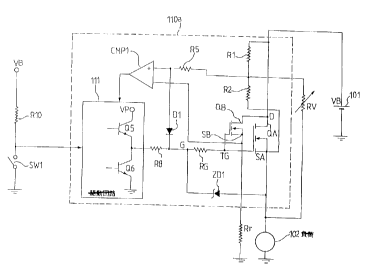
Fig. 1 is a circuit diagram showing a power supply control
device which is a first embodiment of the present invention. Fig.
2 is a circuit diagram showing in detail a semiconductor switch
(MAIN CONTROL FETj used in the embodiment. Figs. 3, 4 and 5 are
explanatory diagrams useful in explaining the principles of the
power supply control device arid the method of controlling the same.
which form a first embodiment of the present invention. Fig. 6
is a waveform diagram showing a current and a voltage in a
semiconductor switch used in the power supply control device when
the power supply control device suffers from short-circuit and it
normally operates. Fig. 7 is a circuit diagram showing a power
supply contzol device which is a second embodiment of the present
invention. Fig. 8 is a circuit diagram showing a power supply
control device which is a third embodiment of the present invention.
Figs. 9 and 10 are circuit diagrams showing a power supply control
device which is a fourth embodiment of the present invention. Figs.
29
CA 02293932 1999-12-29
11 and 12 are circuit diagrams showing a power supply control device
which is a fifth embodiment of the present invention. Figs. 13 and
14 are circuit diagrams showing a power supply control device which
is a sixth embodiment of the present invention. Fig. 15 is a circuit
diagram showing a second load ( res istors ) in a modification of the
power supply control device. Figs . 16 and 17 are circuit diagrams
showing a power supply control device which is a seventh embodiment
of the present invention. Fig. 18 is a circuit diagram showing a
power supply control device which is an eighth embodiment of the
present invention.
Fi rst EmbOdim_gnt
The power supply control device which is the first embodiment
of the present invention will be described with reference to Fig.
1. In the powez supply coritrol device, a drain D - source S,a path
of a main control FET QA as a semiconductor switch is inserted in
series in a path for applying an output voltage VB of a power souzce
101 to a load 1.02. While the main control FETQA is of the NMOS type
in the circuit, it may be of the PMOS type.
In the figure, a circuit section for driving the main control
FETQA contains an REFERENCE FETQB, res,lstors R1, R2, R5, R8, R10,
RG, Rr and RV , a Zener diode ZD1, a diode D1, a comparator CMP1,
a drive circuit I11, and a switch SW1, zn the specification,
capital letters "Rs" with numerals and characters attached thereto
are used for designating the resistors and also their resistance
values. In Fig. 1, a portion enclosed by a dotted line indicates
CA 02293932 2000-03-28
an analog IC chip onto which the circuit components within the
enclosed portion are integrated.
The load 102 includes head lamps, drive motors for power
windows and others. It is operated when a user turns on the
S switch SWl. The drive circuit 111 includes a series circuit of
a source transistor Q5 connected at the collector to a
potential VP, and a sink transistor Q6 connected at the emitter
to ground potential (GND) . In response to an on/off signal of
the switch SW1, the source transistor QS and the sink
transistor Q6 are turned on and off, so that the drive circuit
111 outputs a signal for driving the FETQA. In the figure, VB
indicates an output voltage of 12v, for example. VP indicates
an output voltage of a charge pump. VP is of VB + 10V, for
example.
The detail of the main control FETQA as a semiconductor
switch is as shown in Fig. 2. As shown in Fig. 2, the main
control FETQA includes an internal resistor RG, a temperature
sensor 121, a latch circuit 122, and an overheat cut-off FET
QS. The Zener diode ZD1 keeps the voltage between the gate G
and the source SA of the FET at 12V, and when an overvoltage is
applied to the gate G of FET, it forms a bypass for the
overvoltage flow or progration.
31
CA 02293932 2000-03-28
The main control FETQA of the present embodiment has such
an overheat cut-off function that when the temperature sensor
121 detects that a temperature of the main control FETQA rises
to a predetermined temperature or higher, information of the
high temperature is held in the latch circuit 122 and the
overheat cut-off FET QS as a gate cut-off circuit is turned on
to forcibly turn off the main control FETQA.
The temperature sensor 121 consists of four diodes
connected in series, and when fabricated, it is located near
the main control FETQA. With increase of a temperature of the
main control FETQA, resistance values of those diodes of the
temperature sensor 121 decrease. Accordingly, when a potential
at the gate of a FET Q51 lowers to a potential corresponding to
"L" level, a state of the FET Q51 shifts from an on state to an
off state. As a result, a gate potential of a FET Q54 is pulled
up to a potential at the gate control terminal G of the main
control FETQA, a state of the FET Q54 shifts from an off state
to an on state, and finally "1" is latched in the latch circuit
122. At this time, an output signal level of the latch circuit
122 is an "H" level, and the overheat cut-off FET QS shifts its
state from an off state to an on state. Accordingly, the true
gate TG of the main control FETQA and the source SA of the same
32
CA 02293932 2000-03-28
are at an equal potential. The main control FETQA shifts its
state from an on state to an off state. As a result, the
overheat cut-off operation is effected.
The power supply control device has also protection
function against an overcurrent caused by a short-circuit which
occurs at the load 102 or between the source SA of the main
control FETQA and the load 102, or against an abnormal current
caused by an imperfect short-circuit. A circuit arrangement to
realize the protection functions will be described with
reference to Fig. 1.
Reference voltage generating means, which is used in
claims, is made up of the FET (second semiconductor switch) QB
and the resistor (second load) Rr. The drain and gate of the
REFERENCE FETQB are connected to the drain D and the true gate
TG of the main control FETQA, respectively. The source SB of
the REFERENCE FETQB is connected to one of the terminals of the
resistor Rr, which is connected at the other terminal to ground
potential GND. Thus, the drain D and the true gate TG are used
in common for both the main control FETQA and the REFERENCE
FETQB. This makes it easy to fabricate those FETs into a same
semiconductor chip.
33
CA 02293932 2000-03-28
The main control FETQA and the REFERENCE FETQB are
fabricated on a same chip by a same process. A current
detecting method which is employed in the embodiment, is based
on a detection of a difference between a voltage V DSA across
the drain-source path of the main control FETQA and a reference
voltage, the detection being carried out by the comparator
CMP1. Therefore, with fabrication of the REFERENCE FETQB and
the main control FETQA into the same chip, it is possible to
eliminate (reduce) the error caused by common mode deviation in
the current detection, viz., unwanted effects by drifts of the
power source voltage and temperature, and variations among
different manufacturing lots. Additionally, the mounting of
the resistor (second load) Rr outside the chip 110a makes the
reference voltage insensitive to temperature variations of the
chip 110a, realizing highly accurate current detection. Thus,
the drain D and the true gate TG are used in common for both
the main control FETQA and the SECOND REFERENCE FETQB. This
makes it easy to fabricate those FETs into a same semiconductor
chip.
In order that a current capacity of the REFERENCE FETQB is
smaller than that of the main control FETQA, ratios of the
numbers of parallel-connected transistors which form those FETs
34
CA 02293932 2000-03-28
are selected to be:
(number of transistors of the reference FETQB ., 1
transistor) < (number of transistors of the main control FETQA
. 1000 transistors)
A resistance value of the resistor Rr, as will be
described later, is set to be (resistance value of the load
102) x (number of transistors of the main control FETQA . 1000
transistors/number of transistors of the REFERENCE FETQB . 1
transistor). By setting the resistor Rr so, when a load
current of 5A, which flows when the power supply control device
normally operates, flows through the main control FETQA and a
current 5mA flows through the resistor Rr, the drain-source
voltages VDS of the FET QB is equal to the corresponding one of
the main control FETQA. When the circuit is so specified, the
reference voltage generating means including the REFERENCE
FETQB and the resistor Rr is minimized in size, leading to
reduction of the element fabricating space and cost to
fabricate the device.
A resistance of the resistor R2 is equivalently varied by
varying the resistance of the variable resistor RV.
34a
CA 02293932 1999-12-29
Varying the variable resistor RV in its resistance may
equivalently vary a resistance value of the resistor R2. Voltage
division means, which includes the resistors R1, R2 and Rv, divides
the drain-source voltage VDSA of the main control FETQA at a voltage
division ratio based on a resistance value ratio of those resistors,
and applies the resultant voltage to the comparator CMP1. The
voltage division ratio is varied with the variable resistor RV.
With use of the variable resistor RV, a threshold value of the
drain-source voltage VDS may be varied which is used for switching
the output signal level of the comparator CMP1 from an "H" level
to a "L" level with r espect to a fixed set value (reference
value) of the reference voltage generating means. This enables
a same type of semiconductor chip 110a to cover a plurality of
specifications when the circuit is fabricated into an analog
integrated circuit.
The eomparator CMP1 is involved in "detecting means" , which
is used in setting forth claims . A "+" input terminal of the
comparator CMP1 receives through the resistor R5 a voltage, which
is produced by dividing the drain-source voltage vDSA of the main
control FETQA by a parallel resistance (R2 (~ RV) of the resistor
R2 and the variable resistor RV, which are connected in parallel.
A -" input terminal of the comparator CMP1 receives the
drain-source voltage VDSH of the REFERENCE REFERENCE FETQB. When
a potential at the + input terminal of the comparator CMP1 is higher
than that at the - input terminal, the output of the comparator
CA 02293932 1999-12-29
CMP1 is valid ( "H" level ) . Conversely, when the potential at the
+ input terminal of the comparator CMP1 is lower than that that
at the - input terminal, the output of the comparator CMP1 is invalid
( "1," level ) . As will be described later, the comparator CMP1 has
a hysteresis characteristic.
A method of controlling the thus arranged power supply control
de~rice of the first embodiment of the present invention will be
described. The principles on which the power supply control device
and the method of controlling the same, which are the embodiments
of the invention, are based will be described with reference to
Figs. 3, 4 and 5. Fig. 3 is a graph showing a descending
characteristic curve of a voltage across the drain-source path of
the FET QA when the FET QA shifts its state from an off state to
an on state. Fig. 4 is a circuit diagram showing the concept of
a power supply path ranging from the power source 101 to the load
102. Fig. 5 is a graph useful in explaining a characteristic curve
of a drain current of the thermal FET with respect to the gate-source
voltage.
A power supply path ranging from the power source 101 to the
load 102 may electrically be expressed as shown in Fig. 4 when the
main control FETQA is used for the semiconductor switch. The load
102 includes a wire inductance LO and a wire resistance RO of the
power supply path. When a short-circuit occurs in the power supply
path or the load 102, the wire resistance includes a short-circuit
resistance. The short-circuit resistance is approximately 40 m
36
CA 02293932 2000-03-28
S2 when the dead short-circuit occurs and approximately 40 to
500 MS2 when the layer short-circuit occurs if the load 102 is
head lamps in the motor vehicle to which the present invention
is applied. A curve representative of a voltage across the
drain-source path of the main control FETQA descends as shown
in Fig. 3 when the main control FETQA as a part of the power
supply path shifts its state from an off state to an on state.
The characteristic curve plotted are those of cases where a
short-circuit occurs, the load is a reference load (normally
operates), and the load resistance is 1 K~2.
Thus, the descending characteristic curves varies
depending on states of the power supply path and the load,
viz., a time constant defined by wire inductance and resistance
of the power supply path, and the short-circuit resistance.
Examples of known methods for detecting an overcurrent by
utilizing the characteristic variation of the drain-source
voltage VDS are an overcurrent detecting method described
hereunder and a method for detecting an overcurrent by
comparing the present current value with a predetermined
reference value at predetermined timings. To construct means
for determining the predetermined timings and means for
comparing it with the predetermined threshold value, circuit
37
CA 02293932 2000-03-28
components such as capacitors and resistors are required.
Fluctuation of the value of those circuit components lead to
detection errors. Further, the capacitors, which are
indispensably used, cannot be fabricated into the semiconductor
chip. Therefore, those must be located outside the chip,
leading to increase of the cost to manufacture.
The main control FETQA operates in a pinch-off region till
the main control FETQA shifts its state to an on state and the
drain-source voltage VDS is saturated.
A variation of the drain-source voltage VDS when the load
102 is 1 KS2 may be considered in the following way. Firstly,
when the main control FETQA is, for example, ~~HAF2001",
manufactured by Hitachi Corporation in Japan at power supply
voltage in 12V, the gate-source voltage VTGS is kept at
approximately 1.6 V of the threshold voltage since the drain
current ID - 12 mA. Secondly, the charging of the gate G by
the drive circuit 111 continues. If it continues, the gate-
source voltage VTGS will rise. However, the drain-source
voltage VDS drops and a gate-drain capacity CGD discharges. As
a result, the charge that will reach the gate-source voltage
VTGS is absorbed. In other words, the drain-source voltage VDS
drops to discharge the gate-drain capacity CGD at such a rate
38
CA 02293932 2000-03-28
as to cause the gate-drain capacity CGD to discharge such an
amount of charge as to prevent the charge supplied by the gate
drive circuit from further increasing the voltage of VTGS. .As
a result, the gate-source voltage VTGS is kept at approximately
1.6 V. With the decrease of the gate-drain voltage VTGD, the
drain-source voltage VDS also drops. Two factors to absorb the
charge at this time are present; a first factor is the
discharging of the gate-drain capacity CGD due to the drop of
the gate-drain voltage VTGD, and a second factor is an increase
of the capacitance of the gate-drain capacity CGD due to a
decrease of the depletion layer of the n-region.
The following interpretation may also hold about a
variation of the drain-source voltage VDS when the load 102 is
1 K~2.
From the characteristic curves, one knows such values of
the drain-source voltage VDS that charging electrical charges
to be sent to the true gate TG by the drive circuit 111 are
absorbed and the gate-source voltage VTGS of the true gate TC
is kept constant, at the respective time points following the
turning-on of the main control FETQA.
Accordingly, if after a time lapses, the drain-source
voltage VDS is located above the characteristic curve when
39
CA 02293932 2000-03-28
the load resistance - 1 KS2 the gate-source voltage VTGS is
higher than 1.6 V.
When the amount of charge of ~VDSGAP X CGD is subtracted
from the gate-source voltage VTGS at anytime often turning-on
off FETOA, the gate-source voltage VTGS results in 1.6 V.
Here, ~,VDSGAP represents a distance of the present
characteristic curve measured vertically from the
characteristic curve when the load resistance - 1 KS2 ( Fig. 3 ) .
In other words, the gate-source voltage VTGS has been increased
from 1.6V by this amount of charge. A mathematical expression
of this
20
39a
CA 02293932 1999-12-29
is
VTGS-1. 6=~VDSGAP x2CGD/ (CGS-~-2CGD)
Thus , ~VDSGAP is proportional to ( gate-source voltage VTGS - 1 . 6V ) .
A substantially linear proportional relationship of 1 : 1 is
present between the drain current ID and the gate-source voltage
vTGS, as shown in Fig. 5. The characteristic curve plotted in Fig.
5 is that of "HAF2001~~, manufactured by I~itachi corporation. In
l0 the graph, the gate-source voltage VGS corresponds to the
gate-source voltage vTGS_ ,accordingly, LIvDSGAp represents the
drain current ID on the basis of the relationship as shown in Fig.
5. In Fig. 5, a resolution in the vicinity of ID= 10A is
approximately 60 mV/A. Specifically, when the drain current ID
varies by 1A, the gate-source voltage vTGS varies by 60 mV. When
the drain current ID varies by ~ 5 A, the gate-source voltage VTGS
varies by ~ 0 . 3 V _ In the conventional power supply control device,
this resolution corresponds to a resolution which corresponds to
60 mS2 of the shunt resistance RS.
When the drain current ID is zero, a curve of the drain-source
voltage VDS is determined by only the circuit for charging the gate
and the mirror capacitance. When the drain current ID flows, it
is affected by an inductance LC of the circuit and a resistance
RC of the v~rhole circuit. T~ith increase of the drain current ID,
the curve of the drain-source voltage vD5 rises_ When the dxain
CA 02293932 2000-03-28
current ID greatly increases as in the case of the dead short-
circuit, an ascending slope of the drain current ID shown in
the graph with the horizontal axis of time scale and the
vertical axis of ID current tends to a fixed value, which is
determined by a charging rate of the gate charging circuit.
Therefore, the curve of the gate-source voltage VTGS also
converges. An ascending slope of the drain current ID, which
is determined by a rise of the curve of the gate-source voltage
VTGS when a variation of the gate-drain voltage VTGD is zero,
is a limit slope.
Returning to Fig. 4, description will be given about an
operation of the main control FETQA (the magnitude relation
between a force to vary the drain-source voltage VDS and a
force to vary the drain current ID) when the drive circuit 111
performs an off control.
When the source transistor Q5 in the drive circuit 111 is
shifts its state to an off state and the sink transistor Q6
shifts its state to an on state, the charge stored in the true
gate TG is discharged through the internal resistor RG and a
resistor R8, and the sink transistor Q6.
At this time, even if the gate charge is discharged and
the gate-source voltage VTGS drops, during a time that the main
41
CA 02293932 2000-03-28
control FETQA lies in operation in the ohmic region, the drain
current ID is little influenced by the voltage drop.
At this time, the drain-source voltage VDS also little varies:
When the main control FETQA enters in operation of the
pinch off region, the gate charge discharging will lower the
gate-source voltage VTGS and reduce the drain current ID. At
this time, the drain current ID will maintain its current state
that is set up under the condition determined by the external
circuit. Therefore, the drain-source voltage VDS increases to
charge the gate-drain capacity CGD, so that the electrical
charges discharged from the gate are neutralized, to thereby
eliminate their influence to the drain current ID. This
phenomenon occurs due to the magnitude relation between a force
to maintain the drain current ID and a force to maintain the
drain-source voltage VDS. Specifically, it is caused by the
fact that the former force is considerably larger than the
latter force. Such a covering operation continues within a
range within which the drain-source voltage VDS is variable.
Even if the drive circuit 111 performs an off-control
during the course of increasing of the drain current ID, the
drain current ID continues its increase so long as a variation
(increase) of the drain-source voltage VDS is allowed since the
42
CA 02293932 2000-03-28
drain-source voltage VDS varies (increase). At a time point
where the drain-source voltage VDS is incapable of increasing,
the drain current ID begins to decrease in accordance with the
reduction of the gate source voltage VTGS which is determined
S by only the discharging of the gate electrical charges. In
other words, a stage where the drive circuit 111 performs the
off-control, the drain current ID is little influenced by the
off-control till the variation of the drain-source voltage VDS
terminates. The on/off operation of the main control FETQA is
based on the mechanism mentioned above.
When the gate charging circuit is changed to another gate
charging circuit, the VDS curve also changes for the same load
current. For this reason, it is necessary to always keep the
gate charging current constant. If the gate charging current
is reduced, the VDS curve shifts upward. The overheat cutting-
off operation by the overheat protection function may be
quickened if the drain-source voltage VDS is increased with
respect to the drain current ID by utilizing this nature.
An overheat cut-off quickening circuit (overheat cut-off
quickening means) to be described later is designed by the
utilization of this idea.
An operation of the power supply control device will be
43
CA 02293932 2000-03-28
described on the basis of the considerations thus far made. The
reference voltage generating means (REFERENCE FETQB and
resistor Rr) will first be described. The main control FETQA
and the REFERENCE FETQB form a current mirror circuit of 1000 .
1. When a source potential of the main control FETQA is equal
to that of the REFERENCE FETQB, the drain current IDQA = 1000 x
drain current IDQB.
Therefore, when the drain current IDQA of the main control
FETQA = 5 A and the drain current IDQB of the REFERENCE FETQB =
5 mA, the drain-source voltage VDS of the main control FETQA
is equal to that of the REFERENCE FETQB, and the same thing is
true for the gate-source voltage VTGS~ VDSA=VDSB, and
VTGSA=VTGSB. Here, VDSA and VDSB are drain-source voltages of
the main control FETQA and FETQB, and VTGSA and VTGSB are the
gate-source voltages of the main control FETQA and REFERENCE
FETQB.
Accordingly, when the REFERENCE FETQB is saturated in a on
state, a voltage substantially equal to the output voltage VB
is applied to across the resistor Rr. Therefore, a load of the
REFERENCE FETQB equivalent to a 5 A load connected to the main
control FETQA, viz., resistance of the resistor Rr is: Rr=12
V / 5 mA = 1. 4 ks2 .
44
CA 02293932 2000-03-28
A value (curve) of the drain-source voltage VDS when
current of 5A flows into the main control FETQA is used as a
reference value. The reference voltage generating means ,is
reduced in size and hence a small chip occupying area is
realized by constructing the reference voltage generating means
by using the REFERENCE FETQB of which the transistor ratio (_
current capacity ratio) is small with respect to the main
control FETQA. Further, by fabricating the main control FETQA
and the REFERENCE FETQB on a same chip by a same process,
errors caused by deviation from specified values among
manufacturing rots and temperature drifts are removed, thereby
remarkably improving the detection accuracy.
An operation of the main control FETQA in the pinch off
region will be described. When the main control FETQA shifts
its OFF state to the ON state, the drain current IDQA rises
toward the final load current value, which is determined by the
circuit resistance. The gate-source voltage VTGSA takes a
value determined by the drain current IDQA, and also rises
while being braked by the mirror effect of the gate-drain
capacity CGD, which is due to the lowering of the drain-source
voltage VDSA. Further, the gate-source voltage VTGSB of the
REFERENCE FETQB is determined through the operation of the
CA 02293932 2000-03-28
REFERENCE FETQB as a source follower with the resistor Rr of
1.4 kS2 as its load.
The gate-source voltage VTGSA of the main control FETQA
grows with increase of the drain current IDQA, and hence
VTGSB<VTGSA. Since VDSA=VTGSA+VTGD, and VDSB=VTGSB+VTGD, VDSA-
VDSB=VTGSA-VTGSB. VTGSA-VTGSB as the gate-source voltage
difference indicates IDQA-IDQB as the drain current difference.
Therefore, a difference between the drain current IDQA and the
current IDQB flowing through the reference voltage generating
means is obtained by detecting the difference VTGSA-VTGSB. As
the VDSB becomes small (the VDSA also becomes small), the
current IDQB approaches to 5mA (this value corresponds to IDQA
- 5A ) .
The drain-source voltage VDSB of the REFERENCE FETQB is
directly input to the comparator CMP1, and the drain-source
voltage VDSA of the main control FETQA is divided by the
resistance R1 and the resistance R2 (in this case, resistance
of the variable resistor RV is not considered), and the
resultant is applied to the comparator CMP1. That is, the
voltage applied to the comparator CMP1 is given by
VDSA X Rl/ (R1+R2) ~~~ " (1)
46
CA 02293932 2000-03-28
Immediately after the main control FETQA shifts its state to
the on state, the VDSB of the REFERENCE FETQB > (1). With
increase of the drain current IDQA of the main control FETQA,
the value of the expression (1) decreases but exceeds the
drain-source voltage VDSB. At this time, the output level of
the comparator CMP1 shifts from an "H" level to a "L" level to
turn off the main control FETQA.
The hysteresis characteristic of the comparator CMPl is
formed by the diode D1 and the resistor R5. When the main
control FETQA is turned off, the gate potential is connected to
ground by the sink transistor Q6 of the drive circuit 111, and
a potential difference between the cathode of the diode D1 and
the drain D of the main control FETQA is VDSA + 0.7 V (voltage
drop of the Zener diode ZD1 in the forward direction).
Accordingly, current flows through a path of R1 -> r5 -> D1,
and a potential at the + input terminal of the comparator CMP1
lowers to below that the drive circuit 111 performs the on
control. Accordingly, the main control FETQA maintains the off
state because VDSA-VDSB is lower than that when its state was
shifted to an off state. As both VDSA and VDSB increase and
approach to VB, the condition that expression (1) is smaller
than VDSB is re-established and then it shifts its state to an
47
CA 02293932 2000-03-28
on state. There are a variety of ways of forming the
hysteresis characteristic, the above mentioned one is one
example of those ways.
Assuming that the drain-source voltage VDSA present when
the FET QA is turned off is designated as a threshold value
VDSAth, the following relation holds.
VDSAth-VDSB=R2/Rl X VDSB (at 5 [mA]) ~~~~~ (2)
An overcurrent judging value is given by the equation (2).
To change the overcurrent judging value, the resistance of the
variable resistor RV, which is connected in parallel with the
resistor R2 and which is located outside the chip 110a, is
adjusted. Specifically, the overcurrent judging value may be
reduced by decreasing the resistance of the variable resistor
RV.
An operation of the main control FETQA in the ohmic region
will be described. If the main control FETQA shifts its state
to an on state in a normal wiring state, the main control FETQA
successively maintains the on state. Therefore, the gate-source
voltages VTGSA and VTGSB each reach about 10V, and both the
thermal FETs QA and QB operate in the ohmic region.
47a
CA 02293932 2000-03-28
In this region, the 1 . 1 relation between the gate-source
voltage VGS and the drain current ID is lost. In the case of
10
20
47b
CA 02293932 1999-12-29
"HAF2001~, by Hitachi corporation, the on resistance RDS (ON) _
30 mSZ when VGS =10 v. Then, we have
VDSB=5A X30mS2 - 0. 15V
VDSA= IDQA x 3 0 m S~
VDSA-VDSB=30m~ X (IDQA-5A) -~~-~ (3~
When the drain current IDQA increases by a short-circuit of
the wiring, the value of the equation (3) increases, and when it
exceeds the owercurrent judging value, the main control FETQA is
placed to an off state. Thereafter, the main control FETQA enters
the pinch off region in its operation, and it repeats the on and
off states
Fig. 6 is a waveform diagram showing waveforms of a voltage
and a current in the main control FETQA used in the power supply
control device, which is the present embodimezlt.
Fig. 6 ( a ) shows a wavefarm of the drain current ID (A) , and
Fig. 6(b) shows a waveform of the drain-source voltage VDS_ In
those figures, (2) indicates the wavefoims when the power supply
control device normally operates; and ( 3 ) indicates the waveforms
when an overload condition (including the short-circuit between
the source and the load).
In a case that a overload condition occurs ( wave forms ( 3 ) ) ,
the on/off control of the main control. FETQA, is repeated to cause
the periodic heating of the main control FETQA so as to effect the
overheat protection function.
48
CA 02293932 2000-03-28
As described above, in the power supply control device and
the method of controlling the same, for the current detection,
there is no need of using the shunt resistor connected .in
series to the power supply path, while the shunt resistor is
indispensably used in the conventional power supply control
device. The power supply control device can highly accurately
detect an over current without the shunt resistor.
Additionally, the power supply control device enables the
hardware circuit to successively detect not only the
overcurrent arising from the dead short-circuit but also the
abnormal current arising from the layer short-circuiting having
some short-circuit resistance, such as layer short-circuit.
In the case of the layer short-circuit, the power supply
control device repeats the on/off control of the main control
FETQA to greatly vary the current and to cause a periodic
heating of the semiconductor switch. The periodic heating
quickens the shutting off (off control) of the main control
FETQA by the overheat protection function.
Further, the on/off control of the semiconductor switch can be
effected by use of only the hardware circuit not using the
microcomputer. This feature leads to reduction of the device
mounting space, and remarkable reduction of device
49
CA 02293932 2000-03-28
manufacturing cost.
When comparing with the overcurrent detecting method in
which the characteristic variation of the drain-source voltage
VDS is utilized as in the present embodiment, but the present
current is compared with a predetermined threshold value of
current at predetermined timings, the overcurrent detection of
the embodiment has the following advantages. Such circuit
components as capacitors and a plurality of resistors are
unnecessary. Therefore, there is eliminated detection errors
caused by variations of circuit constants of those components.
Further, there is no need of the capacitor mounted outside the
chip 110a. The result is to reduction of the fabricating space
and device fabricating cost.
With the adjustment of the variable resistor RV, it is
possible to perfectly discriminate between the dead short-
circuit and the layer short-circuit for the type of the load
102 (e. g., headlamps, drive motor, or the like). Protection
against the short-circuit trouble is effected highly
accurately.
Second Embodiment
A power supply control device and a method of controlling
the same, which form a second embodiment of the present
CA 02293932 2000-03-28
invention, will be described with reference to Fig. 7. The
power supply control device of the second embodiment
corresponds to that of the first embodiment additionally having
resistors R3, R4, R6, R9 and FETs Q1 and Q2, and a Zener diode
ZD2. A portion enclosed with a dotted line in Fig. 7 is an
analog IC chip 110b onto which the circuit components within
the enclosed portion are integrated.
The resistor R9 interconnects the gate and the source of
the FET Q1. The true gate TG of the main control FETQA is
connected to the gate of the FET Q1, through the Zener diode
ZD2 and the resistor R6. The drain of the FET Ql is connected
to VB + 5V, through the resistor R4. The source of the FET Q1
is connected to the source SA of the main control FETQA. The
resistor RI is connected in parallel with a circuit in which
the resistor R3 and the FET Q2. A voltage division of the
drain-source voltage VDSA of the main control FETQA is varied
through the on/off control of the FET Q2.
An operation of the power supply control device of the
second embodiment will be described. The operation of it in
the pinch off region will first be described. As in the first
embodiment, the drain-source voltage VDSB of the REFERENCE
FETQB is directly connected to the comparator CMP1. The drain
51
CA 02293932 2000-03-28
source voltage VDSA of the FET QA is divided by a parallel
resistance (RI II R3) of the resistor R1 and the resistor R3,
which are connected in parallel, and the resistor R2 (here, the
variable resistor RV is not taken into consideration), and is
applied to the comparator CMP1.
Specifically, a voltage value given by the following
expression is input to the comparator CMP1.
VDSA X ( Rl I I 1R3 ) / ( ( R- I I R3 ) +R2 ) ~ ~ ~ ~ ( 1' )
Immediately after the FET QA is turned on, VDSB >
where VDSB is the drain-source voltage of the REFERENCE FETQB.
Within crease of the drain current IDQA of the FET QA, the
value (1') the drain-source voltage VDSB of the REFERENCE
FETQB. At this time, the output level of the comparator CMPl
shifts from an "H" level to a "L" level. As a result, the
FETQA is turned off.
Assuming that the drain-source voltage VDSA appearing when
the main control FETQA shifts its state to an off state is
designated as a threshold value VDSAth, then the following
relation holds.
VDSAth-VDSB=R2/ (R1 ~IR3) XVDSB ~~~~ (2')
52
CA 02293932 2000-03-28
An overcurrent judging value is determined by the equation
(2').
To change the overcurrent judging value, the resistance of the
variable resistor RV, which is connected in parallel with the
resistor R2 outside the chip 110b, is adjusted.
Specifically, the overcurrent judging value may be reduced by
decreasing the resistance of the variable resistor RV.
The operation of the power supply control device in the
ohmic region and the operation described with reference to Fig.
6 are substantially the same as those in the first embodiment,
and hence no further description of them will be given.
The overcurrent judging value will be discussed.
It is assumed that the overcurrent judging value for the pinch
off region is equal to that for the ohmic region.
(VDSA-VDSB) /,Q,ID in the pinch off region will first be
calculated. The following relations are derived from the
characteristic curve of the HAF2001.
,QVTGSA/~IDQA=60 [MV/A] ~~~~~(4)
D VTGSA= L~(VDSA-VDSB) X2CGD/ (CGS+2CGD)
_ ~(VDSA-VDSB) X2X1200pF/ (1800pF+2X1200pF)
_ ~(VDSA-VDSB) X 0 ~ 57 ~~~~~(5)
Rearranging the equations (4) and (5), then we have
5 3
CA 02293932 2000-03-28
( OVDSA-VDSB) /DID=105 [mV/A] ~ ~ ~ ~ ~ (6)
From the equation (3), (VDSA-VDSB) / ID in the ohmic
region is
S Q (VDSA-VDSB) /DID=30 [mV/A] ~ ~ ~ ~ (7)
When comparing the equation (6) with the equation (7), a
current sensitivity in the pinch off region is higher than that
in the ohmic region. An overcurrent judgeing value, even if it
is appropriate in the ohmic region, is too small in the pinch
off region. In this case, there is a danger that an
overcurrent detection will frequently occur in this region.
One possible measure to be taken for this is to switch the
overcurrent judging value between the pinch off region and the
ohmic region. This is implemented by the circuit added to the
first embodiment circuitry.
Judgement as to whether the operation region of FET is the
pinch off region or the ohmic region is made by amplitude of
the gate-source voltage VTGSA. With increase of the drain
current ID, the gate-source voltage VTGSA in the pinch off
region grows. In this case, however, it never exceeds 5V even
if a dead short-circuit occurs. Therefore, if VTGSA > 5V, it
is judged that the current operation region of the FET is the
ohmic region.
54
CA 02293932 2000-03-28
Immediately after the FET QA is turned on, the FET Q1 is
in an off state and the FET Q2 is in an on state. To turn on
the FET Q2, a voltage, e.g., + 5V, in excess of the output
voltage VB is required.
Where a breakdown voltage of the Zener diode ZD2 is set at
(5V - 1.6V) (1.6V; threshold voltage of the FET Ql), if VTGSA
(gate-source voltage) > 5V, the FET Ql is turned on and the FET
Q2 is turned off. Then, the resistor R3 coupled in parallel to
the resistor Rl is removed out of the circuit.
Since a division ratio of the drain-source voltage VDSA is
increased, a source-drain voltage difference VDSA-VDSB is which
makes FETQA turn-off is more reduced. As a result, in the
ohmic region, the overcurrent judgement is made at a smaller
current than before the measure is taken.
However, no problem will arise in practical use if the
measure by the additional circuit of the embodiment is not
taken. Specifically, when the final load current value is
small, the current completely rises within the pinch off
region. In other words, the current reaches the final load
current value within the pinch off region when the final load
current is small. When the final load current is large, the
current is still in the middle of rising within the pinch off
region. Even in the case of the dead short-circuit, the
current is limited to within about 40A.
5 5
CA 02293932 2000-03-28
Thus, as the final load current value increases, the
current variation converges to a current rise characteristic
curve having a fixed slope. The difference of the drain-source
voltage VDSA is not so large as one that will be appear when
each load current is fully saturated. Because of presence of
this phenomenon, where the current sensitivity is large in the
pinch off region, the drain-source voltage difference VDSA-VDSB
does not grow large. Accordingly, if the current value in the
reference voltage generating circuit is appropriately selected,
a practical power supply control device with an overcurrent,
protection function is realized by use of the arrangement of
the first embodiment even if the additional circuit as of the
present embodiment is not used.
The thus arranged power supply control device and a method
of controlling the same produce the useful effects comparable
with those of the first embodiment already described in detail.
Finally, a basic concept of the overcurrent control will
concisely be described. Firstly, when the wiring is normal,
the FET QA is turned on and operates in the ohmic region. So
long as the wire is normal, its operation continues in the
ohmic region, and it maintains an on state. When the wiring is
abnormal, the current increases, and when the drain-source
voltage difference VDSA-VDSB exceeds the overcurrent judging
value, the FET QA is turned off and operates in the pinch off
region. So long as the
55a
CA 02293932 1999-12-29
abnormal wiring is present, the FET QA repeats the on and off states,
and continues the operation in the pinch off region, and finally
it is shut off by overheat.
To realize the basic concept and to optimize the overCUrrent
control, it is required that the overcurrent judgizlg value
satisfies the following two conditions. A first condition is that
the FET QA is absolutely not turned off raithir~ the normal current
range. A, second condition is that after the current detected in
the ohmic region is judged to be overcurrent, the FET QA continues
to the on and off states in the pinch off region so long as the
abnormality in the miring is not removed. This is needed for
stabilizing the period of the on/off control. The stabilizing the
period of the on/off control leads to a stability of the control _
A timer is set by use of the period of the on/off control ( see the
sixth embodiment to be described later). Also to this end, the
stabilization of the on/off control period is needed.
To satisfy the first and second conditions, the overcurrent
judging value in the ohmic region is set at a current value of "normal
current maximum value + a" (corresponding to (VDSA - VDSB) , and
2o the overcurrent judging value in the pinch off region is set at
a current value of "normal current maximum value + ,Q~~. At this
time, ~x ~ ,Q . That is, a - ,(3 is an offset quantity necessary to
put the FET operation in the pinch off region.
Third m o imPnt
z5 A power supply control device and a method of controlling the
56
CA 02293932 2000-03-28
same, which form a third embodiment of the present invention,
will be described with reference to Fig. 8. A power supply
control device of this embodiment is different from that of the
power supply control device of the second embodiment (Fig. 7)
in that the gate of the REFERENCE FETQB is not connected to the
true gate TG of the FET QA, and a resistor R41 is additionally
used as a gate resistor of the REFERENCE FETQB. The resistor
R41 is connected at one end to the gate of the REFERENCE FETQB
and at the other end to the gate G of the FET QA. The
remaining circuit construction of the power supply control
device of the embodiment is substantially the same as of the
Fig. 7 circuit construction. In Fig. 8, a portion enclosed by
a dotted line indicates an analog IC chip onto which the
circuit components within the enclosed portion are integrated.
It is required that the resistance of the resistor R41 is
set at 1000. When RG - lOKS2, for example, R41 =lOMS2. Since
the resistance is extremely high, it is preferable, when the
productivity is taken into consideration, that the ratio of the
numbers of transistors is set at 1 . 100, and R41=1MS2.
The operation of the power supply control device of this
embodiment is substantially equal to that of the power supply
control device of the second embodiment, and produces useful
effects comparable with those by the power supply control
device of the first embodiment.
57
CA 02293932 2000-03-28
Fourth Embodiment
A power supply control device and a method of controlling
the
15
25 57a
CA 02293932 1999-12-29
same, which form a fourth embodiment of the pzesent invention, will.
be described with reference to Figs. 9 and 10. The power supply
control device of this embodiment is directed to improvement of
the voltage di~criding means (R1, R2 and RV) in the circuitry of the
power supply control device of the first embodiment ( Fig. 1 ) . As
recalled, the voltage dividing means divides the drain-source
voltage VDSA of the FET QA at a voltage division ratio based on
the resistance value ratio and applies the divided voltage to the
comparator CMP1. A portion 110a' enclosed by a dotted line in Fig.
9 and a portion 110a" enclosed by a dotted line in Fig. 10 indicate
analog IC chips onto which the circuit components within the
enclosed portions are integrated.
Fig. 9, in the power supply control device of this embodiment,
the drain D and source SA of the FET QA are inserted in series in
the path for applying the output voltage vB of the power source
101 to the load 102. A circuit section for driving the FET QA
includes an REFERENCE FETQB, a traps istor Q7 , res istors R1 to R6 ,
R8 to R10, RG, Rr, a Zener diode ZD1, diodes D1 to D3, a comparator
CMP1, a drive circuit 111 and a switch SWI. The FET QA as the
semiconductor switch, which is used in this embodiment, has a
construction as shown in Fig. 2 as in the first embodiment. The
functions and operations of the comparator CMP1, the drive circuit
111 and the switch SW1, and the generation of a reference voltage
by the REFERENCE FETQB and the resistor Rr are also as in the first
embodiment.
58
CA 02293932 1999-12-29
The functions and operations of a circuit portion (transistor
Q~, resistors R1 to R6, and diodes D2 and D3 ) , which are different
from the corresponding one in the power supply control device of
the first embodiment (Fig. 1) will be described.
The PNP transistor Q7 connected between the power source 101
and the res istor Rl is provided for coping with the dark current .
In the power supply control device of the first embodiment (Fig.
1 ) , a dark current path ranging from the power source 101 t.o the
load 102 by way of the resistors R1 and R2 of the voltage dividing
means even when an instruction to supply electric pocuer to the load
102 is not issued, viz., when the FET QA is not driven. Therefore,
even during the off state of the switch SW1, a little electric power
of the power source 101 is consumed.
To reduce the power consumption of the power source 101 by
the dark current, the transistor Q7 is provided and arranged such
that only when the switch SWl is turned on ( an instruction to supply
power source to the load 102 is issued) , the transistor Q7 is turned
on . That is , when the switch SW1 is not turned on, the trans istoz
Q7 is placed in an off state, to thereby cut off the path of the
dark current. Thus, when the transistor Q7 is in the off state,
the current which otherwise flows through a path of R1 (resistor)
R3 (resistor} -~ R2 (resistor) ~ GND (ground), a path of R1
( resistor ) -3 D3 ( diode ) ~ R5 ( resistor ) ~ load 102 -j GND ( ground ) ,
and a path of R1 (resistor) -~ R3 (resistor) -~ D2(diode) ~ R6
(resistor) ~ Rr (resistor) -j GND (ground).
S9
CA 02293932 1999-12-29
The resistors Rl to R6, and diodes D2 and D3 make up a diode
clamp circuit. Assuming that a potential at the node of the
resistors Rl and R3 is vC, and a potential at the node of the resistors
R3 and R2 is VE, VC > VE when the transistor Q7 is in an on state.
If VSA > VC-0. 7V (vSA . source voltage of the FET QA) , the
source voltage VSA is input to the "+'~ input terminal of the
comparator CMP1. If VSA<VC-0.7V, the voltage of "VC-0.7V~~ is
input to the "+'~ input terminal of the comparator CMP1, irrespective
of the source voltage VSA. In other words, even of the source
voltage VSA drops, the "+" input terminal of the comparator CMP1
is clamped at "VC -0-7V", and does not lower below that vol.tage_
The "-" input terminal of the comparator CMP1 is also clamped at
"VE-0. 7V", even if the source voltage VSB of the REFERENCE FETQB
drops below " VE - 0 . 7 V'~ .
With provision of the diode clamp circuit, even when the FET
QA and the REFERENCE FETQB are turned off and the source voltages
VSA and VSB drop, the "+" and "-" input terminals of the comparator
CMP1 are clamped at (vC-0.7V) and (VE-0.7V) . Since VC > VE, the
output signal level of the comparator CMP1 is set at an "H" level,
and hence the FET QA may reliably be turned on independently of
the amplitudes of the source voltage v5 and the source voltage VB.
Further, the voltage withstanding of the "+'~ and "-" input terminals
of the eomparator CMP1 is improved since the potentials at those
input terminals of the comparator CMP1 never drop below a
predetermined value of potential.
CA 02293932 1999-12-29
In the power supply control device of Fig. 10, the gate of
the REFERENCE FETQH is not Connected to the txue gate TG of the
FET QA, and a resistor R41 is additionally used as a gate resistor
of the REFERENCE FETQH. The resistor R41 is connected at one end
to the gate of the REFERENCE FETQs and at the other end to the gate
G of the FET QA. The setting of the resistor R41 and others are
the same as those in the third embodiment already described.
Fifth Embod~m n
A power supply control device and a method of controlling the
1o same, which form a fifth embodiment of the present invention, will
be described with reference to Figs. 11 and 12. A power supply
control device of this embodiment corresponds to the power supply
control device of the first embodiment (Fig. I) to which a rush
current mask circuit 105 and an overheat cut-off quickening circuit
I06 are added. A portion 110d enclosed by a dotted line in Fig.
11 and a portion 110d' enclosed by a dotted line in Fig. 12 indicate
analog IC chips onto which the circuit components within the
enclosed portions are integrated.
when the load x,02 (e. g., head lamps) is turned on, a rush
current flows through the power (source) supply control device.
A value of the rush current amounts to several to several tens times
as large as a current value the current flowing in a stable state
of the circuit. a period of time of the flowing of the rush current
depends on a type and capacity of the 7_oad 102, usually 3 to 20
msec. If the overcurrent control as described in the first, second
61
CA 02293932 2000-03-28
or third embodiment is performed during the rush-current
flowing period, some time is taken till the load 102 settles
down. This appears as unwanted phenomena; the turning on of'the
head lamp delays and a response of the load per se is slow.
This embodiment solves the problem by adding the rush current
mask circuit 105 ("inhibiting means" in claims) to the circuit
of Fig. 1.
In the first, second, third or fourth embodiment, when an
overcurrent arising from a dead short-circuit is detected, the
overheat protection function operates to cut off the FET QA
(off control). In the case of the layer short-circuit, the
on/off control of the FET QA is repeated. The resultant
periodic heating of the FET QA makes the overheat cutting-off
function effective. Accordingly, a time taken for the cutting-
off function to be effective will be relatively long. In the
present embodiment, the overheat cut-off quickening circuit 106
(overheat cut-off quickening means) quickens the cutting off of
the FET QA even in the case of the layer short.
In Fig. 11, the rush current mask circuit 105 includes the
FETs Q11 and Q12, a diode D11, resistors R11 to R13, and a
capacitor C11.
An operation of the rush current mask circuit 105 will be
described. When the FET OA is turned on, the gate-source
62
CA 02293932 2000-03-28
voltage VGSA is applied through the diode D11 and the resistor
R12 to the gate of the FET Q12, and also to the gate of the FET
Q11 through the diode D11 and the resistor R11.
10
20
62 a
CA 02293932 1999-12-29
The gate of the FET QI2 is connected to the source SA of the
FET QA. Immediately after the FET QA is turned on, the capacitor
C11 is not yet charged. Accordingly, a gate potential of the FET
Q12 insufficiently rises, arid the FET Q12 fails to shift its state
to an on state. The FET Q11 maintains its on state during the off
state of the FET Q12, and couples the "--" input terminal of the
comparator cMPl with the source SA of the FET QA. Therefore, the
output level of the comparator CMP1 is kept at an "H" level., and
in this state the FET QA is not tuzned off if a large rush current
flows.
with time lapse, charging of the capacitor C11 through the
resistor R12 progresses, and finally the FET Q12 shifts its state
to an on state. With the turn on of the FET FET Q12, the FET Q11
is turned off and the xttasking state terminates, and the overcurrent
detecting control functions.
The zesistor R13 is a discharging resistor for dischazge and
resetting the capacitor C11 after the FET QA is turned off . In this
case, selection of R12 « R13 is desirable in order that the
discharging operation of the capacitor C11 does not affect the mask
time. The mask time is determined by a time constant of R12 x C11 .
This implies that when the circuit is fabricated into one chip,
the mask time may be adjusted by properly changing the capacitance
of the capacitor C11.
The overheat cut-off quickening circuit 106 is made up of FET
Q21 to Q24, diodes D21 and D22, a Zenez diode ZD21, and resistors
63
CA 02293932 2000-03-28
R21 to R27.
An operation of the overheat cut-off quickening circuit
106 will be described. The power supply control device is
placed to an overcurrent control mode, the gate drive circuit
periodically performs an on/off control, and the gate potential
of the FET QA becomes the potential of an "L" level. During
this time period with the source voltage VSA being in some
amount of voltage, a capacitor C21 is charged through the
transistors Q22 and Q24 and the resistor R22. The gate
potential of the FET Q21 is below a threshold value in an
initial stage. With progress of charging the capacitor C21, the
gate potential rises and the FET Q21 is turned on.
Current flows from the terminal TG (true gate of the FET
QA) to ground (GND) by way of the resistor R21, and electrical
charges stored in the terminal TG is decreased in amount.
Therefore, the drain-source voltage VDSA increases also with
respect to the load resistor. Power consumption by the FET QA
increases to quicken the overheat cutting off operation. The
smaller the resistance of the resistor R21 is, the faster the
overheat cutting-off operation is. The resistor R23 is a
discharging resistor for the capacitor C21. Selection of R22
« R23 is preferable.
64
CA 02293932 2000-03-28
The power supply control device shown in Fig. 12
corresponds to the power supply control device of the fourth
embodiment (Fig.9) to which a rush current mask circuit 105'
and an overheat cut-off quickening circuit 106' are added. The
circuit arrangements of the rush current mask circuit 105' and
the overheat cut-off quickening circuit 106' and the operations
of them are substantially the same as those of the
corresponding ones shown Fig. 11.
Sixth Embodiment
A power supply control device of a sixth embodiment of the
present invention will be described with reference to Figs. 13
and 14. The power supply control device of this embodiment
corresponds to the power supply control device of the first
embodiment (Fig. l) in which an on/off-time accumulating circuit
107 is additionally used. A portion 110e enclosed by a dotted
line in Fig.l3 and a portion 110e' enclosed by a dotted line in
Fig. 14 indicate analog IC chips onto which the circuit
components within the enclosed portions are integrated.
In the first, second, third or fourth embodiment, in the
case of the layer short-circuit, the on/off control of the FET
QA is repeated, and the resultant periodic heating action of
the FETQA causes the overheat cutting-off to function.
Therefore, a time taken for the cutting off function to be
effective is relatively long. This problem is solved by this
65
CA 02293932 2000-03-28
embodiment in the following manner. To be specific, an on/off-
time accumulating circuit (time control means) 107 for causing
the power supply control device to perform the off control when
the number of on/off controls of the FET QA reaches a
predetermined number is additionally used, whereby the cutting
off of the FET QA is quickened.
In Fig. 13, the on/off-time accumulating circuit 107 is
made up of transistors Q31 to Q34, diodes D31 to D33, a Zener
diode ZD31, resistors R31 to R37, and a capacitor C31.
An operation of the on/off-time accumulating circuit 107
will be described. The power supply control device is placed
to the overcurrent control mode, the capacitor C31 is charged
through the transistors Q32 and Q34 and the resistor R32 every
time the off-control is performed (the gate potential is set at
an "L" level) during the on/off operations of the FET QA. The
capacitor C31 is charged only when the drain-source voltage
VDSA is set at the "H" level during the off-control (the gate
potential is set at the "L" level). When the on- or off-
control is consecutively performed, it is not charged. The
gate potential of the FET Q31 is below a threshold value and
hence it is in an off state. When the gate potential rises
with progress of the charging of the capacitor C31, the FET Q31
is turned on. At this time, anode of a temperature sensor 121
(consisting of four diodes) is lowered in potential. As a
6 6
CA 02293932 2000-03-28
result, the same condition as at high temperature is set up,
the overheat cut-off FET QS is turned on, and the FET QA is cut
off (off-control).
A cut-off time by the on/off time accumulation is
preferably about 1 second. To stably operate the on/off-time
accumulating circuit 107, it is necessary to stabilize the
on/off control period of the FET QA. In the present
embodiment, a variation of the drain-source voltage VDSA of the
FET QA with respect to a variation of the load current in the
pinch off region is greater than that in the ohmic region.
Because of this, it is turned off in the pinch off region
during the on/off control (there is no case that it is turned
off in the ohmic region following the pinch off region).
Accordingly, the period of the on/off control of the FET QA is
stable .
In the power supply control device of the present
embodiment, in the on/off-time accumulating circuit 107, the
number of on/off controls of the FET QA is judged by an amount
of electric charge stored in the capacitor C31. Alternatively,
the on/off-time accumulating circuit may be constructed by use
of a counter which directly counts an output signal of the
drive circuit 111. In this case, when a count value of the
counter for counting the output signal of the drive circuit 111
reaches a predetermined value, the overheat cut-off FET QS is
67
CA 02293932 2000-03-28
turned on to cut off the FET QA (off control).
Fig. 14 is a circuit diagram showing a circuit arrangement
in which an on/off-time accumulating circuit 107' is added, to
the power supply control device of the fourth embodiment. The
circuit arrangement and operations of the on/off-time
accumulating circuit 107 are substantially the same as those of
the fourth embodiment of the invention (Fig. 9).
Additionally, in the power supply control device of the
sixth embodiment (as shown in Figs. 13 and 14), after counting
the output signal by the on/off-time accumulating circuit 107,
the overheat cut-off function, which is constituted of the
temperature sensor 121, a latch circuit 122 and the overheat
cut-off FETQS (as shown in Fig. 2), controls the main control
FETQA to the OFF state. However, the present invention could
employ the following modification.
Namely, according to a first modification, the drain of the
FETQ31 is connected to the real gate (TG) of the main control
FETQA via a series circuit of a diode and a resistor. In a
second modification, the prohibited gate (binary input AND
gate) is provides on the output of the comparator CMP1 and the
drain voltage of the FETQ31 is used for prohibited control
signal.
Additionally, in a third modification, the drain of the
FETQ31 is connected to ~~+" input terminal of comparator CMP1
68
CA 02293932 2000-03-28
via a series circuit of a diode and a resistor.
In these modifications, the resistor R31 will be omitted,
and in order to keep the information such that the on/off-t~.me
accumulating circuit 107 cuts off the main control FETQA, the
latch circuit which is composed of a PMOSFET and resistors must
be added.
The source of the PMOSFET is connected to power supply
voltage VB and the drain of the PMOSFET is connected to the
gate of the FETQ31, and then the gate of the PMOSFET is
connected to the drain of the FETQ31 and the source of itself
via resistors respectively.
A modification of the a power supply control device and a
method of controlling the same, which are each of the first to
sixth embodiments, will be described with reference to Fig. 15.
In each of the above-mentioned embodiments, the reference
voltage generating means is set a fixed voltage value. When
the load is varied, the reference voltage generating means
copes with the load variation by correspondingly varying the
overcurrent judging value.
Specifically, the resistances R1 to R3 are set in
accordance with the maximum load used when those are fabricated
into a semiconductor chip. When the load 102 is small, the
variable resistor RV is located outside the chip while being
connected in parallel with the resistor R2, whereby the
6 9
CA 02293932 2000-03-28
overcurrent judging value is lowered.
This method has the following problems. A first problem
is that control accuracy decreases with increase of the
overcurrent judging value. A second problem is that it is
S necessary to change the overcurrent judging value between the
pinch off region and the ohmic region. In this case, the
overcurrent judging value for the pinch off region, to be
exact, must be set in accordance with an ascending slope of the
drain current ID. An ascending slope of the drain current ID
varies when the wire inductance and the wire resistance vary.
It is difficult to accurately set the overcurrent judging
value.
To cope with this, it is effective to set the reference
voltage generating means in accordance with the load 102. To
this end, the reference voltage generating means is set to a
voltage value corresponding to a current value in excess of the
maximum current value of the load 102.
When the drain-source voltage on the load drive transistor
(i.e., the drain-source voltage VDSA of the FET QA) exceeds the
drain-source voltage VDS of the reference voltage generating
means (i.e., the drain-source voltage VDSB of the REFERENCE
FETQB), even if its excess is minute, it is judged that it is
an overcurrent value.
7 0
CA 02293932 2000-03-28
In this method, the same overcurrent judging value may be
used for both the pinch off region and the ohmic region. In
other words, even if the operation region of the FET shits
from the pinch off region to the ohmic and vice versa, there is
no need of changing the overcurrent judging value. Further, in
the method, the overcurrent may be judged by judging whether or
not the drain-source voltage of the load drive transistor
exceeds the drain-source voltage VDS of the reference voltage
generating means. Therefore, its detection accuracy is
determined by only the resolution of the comparator CMPl.
Further, there are eliminated adverse effects by
temperature drift, variations among different IC lots, wiring
inductance and wiring resistor, and it is not affected by a
power source voltage variation so long as the comparator CMP1
normally operates. Thus, a power supply control device and a
method of controlling the same, which have few error factors
(substantially free from error factors), are successfully
realized.
The methods of setting reference voltage generating means
and of changing the setting thereof may be summarized as
follows:
a) The external variable resistor RV is connected in
parallel with the resistor Rr.
71
CA 02293932 2000-03-28
,...
b) The resistor Rr is located outside the chip, and it is
used for setting the reference voltage generating means and
selecting related values in accordance with the specification
used.
c) A resistance of the resistor Rr is varied.
As shown in Fig. 15, a plurality of resistors Rrl to Rr4
is disposed in parallel within the chip. In the stage of chip
packaging or the pair chip mounting, the set value (reference)
of the reference voltage generating means may be set to a
target specification by selecting a proper one of those
resistors by means of a switch SW2. With this, in integrating
the power supply control device onto a semiconductor chip, one
chip may cover a plurality of specifications. With the
variable setting of the variable resistor RV, it is possible to
perfectly discriminate between the dead short-circuit and the
layer sort-circuit for the type of the load 102 (e. g., head
lamps, drive motor, or the like). Protection against the
short-circuit trouble is effected highly accurately.
Seventh Embodiment
A power supply control device according to a seventh
embodiment of the present invention will be described with
reference to Figs. 16 and 17.
The power supply control device of Fig. 16 corresponds to
the power supply control device of the fourth embodiment (Fig.
7 2
CA 02293932 2000-03-28
9) in which the thermal FETs QA and QB are of the p-channel
type. The power supply control device of Fig. 17 corresponds
to the power supply control device of the fourth embodiment
(Fig. 9) in which the thermal FETs QA and QB are IGBTs
(insulated gate bipolar transistors). A portion 110ap enclosed
by a dotted line in Fig. 16 and a portion 110ai enclosed by a
dotted line in Fig. 17 indicate analog IC chips onto which the
circuit components within the enclosed portions are integrated.
Eighth Embodiment
A power supply control device and a method of controlling
the same, which form an eighth embodiment of the present
invention, will be described with reference to Fig. 18. The
power supply control device of this embodiment is a power
supply control device having such a circuit arrangement that a
too-small or minute current detecting function is applied to a
circuitry formed by composing the power supply control devices
of the first, fifth and sixth embodiment.
The drain D and the source S of a FET QA as a
semiconductor switch is inserted in series in a path for
applying the output voltage VB of the power source 101 to the
load 102. In Fig. 18, a section for driving the main control
FET QA contains reference FETs QB and second reference QC, R1,
R2, R5, RG, R10, Rrl, Rr2, a Zener diode ZDl, a diode D1,
compactors CMP1 and CMP2, a drive circuit 111, and a switch
7 3
CA 02293932 2000-03-28
SWl. In Fig. 18, a portion enclosed by a dotted line indicates
an analog IC chip onto which the circuit components within the
enclosed portion are integrated.
The FET QA as the semiconductor switch, as in the first
embodiment, is constructed as shown in Fig. 2. The functions
and operations of a charge pump 305, a cut-off latch circuit
306, a comparator CMP1, a drive circuit 111, a switch SW1 and
others, and the generation of a reference voltage by the
REFERENCE FETQB and the resistor Rr are also similar to those
in the first embodiment. A masking circuit 303 for avoiding
the judgement of the rush current flow is substantially the
same as the rush current mask circuit 105 in the fifth
embodiment. An on/off-time accumulating circuit 304 for
performing a cut-off control by accumulating the number of
on/off operations is substantially the same as of the on/off-
time accumulating circuit 107 in the sixth embodiment.
The circuit section (SECOND REFERENCE FETQC, resistor Rr2,
comparator CMP2) for realizing the additional minute current
detecting function will now be described about the circuit
function and operation.
The FET (third semiconductor switch) QC and the resistor
(third load) Rr2 are involved in the word "second reference
voltage generating means" used in claims. The drain and gate
of the SECOND REFERENCE FETQC are respectively connected to the
7 4
CA 02293932 2000-03-28
drain D and the true gate TG of the FET QA. The source SC of
the SECOND REFERENCE FETQC is connected to one of the terminals
of the resistor Rr2. The other end of the terminals of 'the
resistor Rr2 is connected to ground (GND). Thus, the drain D
S and the true gate TG are used in common for both the thermal
SECOND REFERENCE FETQC and the FET QA. This makes it easy to
fabricate those FETs into a same semiconductor chip.
The SECOND REFERENCE FETQC and MAIN CONTROL FET QA, like
that (REFERENCE FETQB) in the first embodiment, are fabricated
on the same chip by the same process. A current detection, as
in the first embodiment, is based on a detection of a
difference between a voltage V DSA across the drain-source path
of the main control FETQA and a reference voltage, and a second
reference voltage, the detection being carried out by the
comparators CMPI and CMP2. Therefore, fabrication of the FETs
QA, QB and QC into the same chip will eliminate (reduce) the
error caused by common mode deviation in the current detection,
viz., unwanted effects by drifts of the power source voltage
and temperature, and variations among different manufacturing
lots. Additionally, the mounting of the resistor (second load)
Rrl and resistor (third load) Rr2 outside the chip 110af makes
the reference voltage insensitive to temperature variations of
the chip 110f, realizing highly accurate current detection.
In order that a current capacity of the SECOND REFERENCE
7 5
CA 02293932 2000-03-28
FETQB is smaller than that of the main control FETQA, ratios of
the numbers of parallel-connected transistors which form those
FETs are selected to be:
(number of transistors of the SECOND REFERENCE FETQC: 1
transistor) < (number of transistors of the main control FETQA:
1000 transistors)
A resistance value of the resistor Rr2 is set to be
(resistance value of the load 102 when an extremely small
current flows) x (number of transistors of the main control
FETQA . 1000 transistors/number of transistors of the SECOND
REFERENCE FETQC . 1 transistor).
The comparator CMP2 forms a part of "second detecting
means" used in claims. The source voltage VSA of the FET QA is
applied to the "+" input terminal of the comparator CMP2, and
the source voltage VSC of the SECOND REFERENCE FETQC is applied
to the "-" input terminal of the same. When a potential
applied to the "+"input terminal is higher than that at the "-"
input terminal, the output of the comparator is valid ("H"
level) . When a potential applied to the "+" input terminal is
lower than that at the "-" input terminal, the output of the
comparator is valid ("L" level) .
Finally, the features and useful effects of the a power
supply control device and a mezthod of controlling the same,
which form the eighth embodiment of the present invention, will
CA 02293932 2000-03-28
be given. Firstly, there is no need of using the shunt
resistor for current detection, and this leads to reduction of
power consumption by the power source supply path. This
feature is useful when it is applied to a large current
circuit. Secondly, a dynamic detecting system is employed which
utilizes the pinch of region of the semiconductor switch (FET
QA). Because of this, a current sensitivity is high
(approximately 105mV/A), and hence current detection accuracy
is high. Thirdly, the on/of control of the semiconductor
switch (FETQA) can be performed with a simple drive control.
Use of the overheat cut-off function and the on/off-time
accumulating circuit 304 realizes a high-speed processing when
comparing with a software (program) using a microprocessor.
Fourthly, one chip fabrication of the circuitry is easy, and if
so done, the device circuit is small, the mounting space is
reduced, and cost to manufacture is reduced. Fifthly, the
current detection is based on the detection of a difference
between the drain-source voltage VDSA of the FETQA and the
reference voltage, and the second reference voltage.
Therefore, fabrication of the FETs QA, QB and QC into the same
chip will eliminate the error caused by common mode deviation
in the current detection, viz., unwanted effects by drifts of
the power source voltage and temperature, and variations among
different manufacturing lots.
CA 02293932 2000-03-28
As described above, in a power supply control device and a
method of controlling the same, which are constructed according
to the present invention, when the power supply from the power
source to the load is controlled in a switching manner by the
semiconductor switch, reference voltage generating means
(reference voltage generating step) generates a reference
voltage having a voltage characteristic substantially
equivalent to that of a voltage between the terminals of the
semiconductor switch being connected to a predetermined load.
Detecting means (detecting step) detects a difference between
the voltage between the terminals of the semiconductor switch
and the reference voltage. Control means (control step)
performs an on/off control of the semiconductor switch in
accordance with the difference between the voltage between the
terminals of the semiconductor switch and the reference
voltage. The reference voltage generating means includes a
circuit connected in parallel with the semiconductor switch and
the load, the circuit containing a series circuit consisting of
a second semiconductor switch and a second load, and generates
a voltage between the terminals of the second semiconductor
switch as the reference voltage. An offset of a voltage
between the terminals of the semiconductor switch (viz.,
current of the power supply path) as a part of the power supply
path, from a normal one is judged by detecting a difference
7 8
CA 02293932 2000-03-28
between a voltage between the terminals of the semiconductor
switch and a reference voltage generated by the reference
voltage generating means (reference voltage generating step).
Accordingly, there is no need of the shunt resistor connected
in series to the power supply path, while the shunt resistor is
indispensably used in the conventional power supply control
device. Further, the heat loss of the device maybe suppressed.
Additionally, the power supply control device enables the
hardware circuit or a software process by the microcomputer to
successively detect not only the overcurrent arising from the
dead short-circuit but also the abnormal current arising from
the layer short-circuit, such as an imperfect short-circuit
having a certain amount of resistance occurs. In particular
when the on/off control of the semiconductor switch is
constructed by a hardware circuit, there is no need of the
microcomputer, and this leads to reduction of the mounting
space and device manufacturing cost.
78a
CA 02293932 1999-12-29
In the invention, second reference voltage generating means
includes a circuit, connected in parallel with the semiconductor
switch and the load, containing a series circuit consisting of a
third semiconductor switch and a third load, and generates a voltage
between the terminals of the third semiconductor switch as a second
reference voltage, and second detecting means detects a difference
between the voltage between the terminals of the semiconductor
switch and the second reference voltage. Therefore, the second
detecting means detects a too-small or minute current if a voltage
characteristic of the reference voltage of the second reference
voltage generating means is substantially equivalent to a voJ.tage
characteristic in a state that a target current, which is below
a minimum current within a normal operation range, flows into the
semiconductor switch and the load.
In the invention, a current capacity of the second or third
semiconductor switch is smaller than that of the semiconductor
switch, and a resistance ratio of the load and the second or third
load is substantially inversely proportional to a current capacity
ratio of the semiconductor switch and the second or third
semiconductor switch. Therefore, the circuit constructions of the
reference voltage generating means including the second
semiconductor switch and the second load and the second reference
voltage generating means including third semiconductor switch and
the third load are reduced in size. This leads to reduction of the
packaging space and device manufacturing cost.
79
CA 02293932 1999-12-29
In the invention, tenth power supply control device, the
second or third load includes a plurality of resistors, and those
resistors are selectively connected or a variable resistor is
connected in parallel to the second or third load. Resistance of
the second or third load is equivalently varied by varying the
resistance of the variable resistor. The voltage between the
terminals of the semiconductor switch is divided by the voltage
dividing means at a voltage division ratio based on the resistance
ratio, and the resultant is applied to the detecting means. With
l0 this, one chip may cover a plurality of specifications _ ,p,,nd zt is
possible to perfectly discziminate between the dead short-circuit
and the imperfect short-circuit for the type of the load.
Protection against the short-circuit trouble is effected with high
precision.
In the invention, overheat protecting means (overheat
protecting step) is fuzther pzovided for protecting the
semiconductor switch by performing an off-control of the
semiconductor switch when the semiconductor switch is excessively
heated. When an imperfect short-circuit having some short-circuit
resistance occurs, the control means (control step, viz. , the off
control step and on control step) repeats the on/off control of
the semiconductor switch to greatly vary the current. At this time,
the semiconductor switch is periodically heated to quicken the
cutting off of the semiconductor switch by the overheat protecting
means (overheat protectingstep)_ In the conventional powersupply
CA 02293932 2000-03-28
control device, only the software process using the
microcomputer, for example, is permitted for dealing with the
abnormal current caused when the layer short-circuit occurs.
On the other hand, the power supply control device of the
S invention can deal with the abnormal current by the hardware
circuit contained therein, not the external control using the
microcomputer. This feature leads to simplification of the
circuit and reduction of manufacturing cost. With this, a high
response to the abnormal current at the time of the imperfect
short-circuit is realized.
In the invention, the semiconductor switch, the second
semiconductor switch, the reference voltage generating means,
the detecting means, the control means, the second reference
voltage generating means, the second detecting means or the
overheat protecting means are integrated onto a single chip.
This leads to reduction of the device circuit construction,
mounting space, and manufacturing cost. A current detecting
method of the invention is based on the detection of a
difference between a voltage between the terminals of
semiconductor switch and a reference voltage or the second
reference voltage, which is carried out by the detecting means
or the second detecting means. Therefore, with fabrication of
the semiconductor switch and the second or third semiconductor
81
CA 02293932 2000-03-28
switch on a same chip, it is possible to eliminate (reduce) the
error caused by common mode deviation in the current detection,
viz., unwanted effects by drifts of the power source voltage
and temperature, and variations among different manufacturing
lots. Additionally, the mounting of the second or third load
outside the chip makes the reference voltage or the second
reference voltage insensitive to temperature variations of the
chip, realizing highly accurate current detection.
In the invention, the period of the on/off control of the
semiconductor switch by the control means is used as a control
clock signal. With this feature, there is no need of using an
oscillating circuit used exclusively for the clock signal
generation. Since the period of the on/off control of the
semiconductor switch (FET) is stable, and a stable clock signal
is produced.
In the invention, inhibiting means (inhibiting step) is
further provided for inhibiting the control means =rom
performing the on/off control by the semiconductor switch
during a fixed time period after the semiconductor switch is
turned on. It inhibits the overcurrent control when a rush
current flows at the start of the load. A slow Of the load
response is reduced.
82
CA 02293932 2000-03-28
In the invention, overheat cut-off quickening means
(control step) is further provided for quickening the off
control by the overheat protecting means (overheat protect~.ng
step) when the control means performs the on/off control of the
semiconductor switch. Therefore, it quickens the cutting off
of the semiconductor switch at the time of the layer short-
circuit, and a quick response is realized.
Further, in the invention, time control means (time
control step) is further provided which operates such that the
time control means accumulates the number of on/off controls of
the semiconductor switch by the control means (in control
step), and when the number of on/off controls reaches a
predetermined number of times, the time control means performs
an off control of the semiconductor switch. Therefore, even in
the case of the layer short-circuit, the cutting off of the
semiconductor switch is quickened and the switch is cut off at
a preset time.
83