Note: Descriptions are shown in the official language in which they were submitted.
CA 02293956 2002-11-06
BACKGROUND OF THE INVENTION
Electronic equipment often employs a circuit board or
interconnection panel such as a backplane, and to which
one or more circuit boards, often called daughter boards,
are connected. The daughter boards are disposed
perpendicular to the backplane and are connected thereto
by mating connectors. The connector on the daughter board
is typically an edge card connector which is disposed
along one edge of the board and which provides electrical
interconnection from contact pads on a surface of the
board to connector contacts in the edge card connector.
This connector is mateable to a complementary connector
mounted on the backplane. The edge card connectors are
separately manufactured components which add to the cost
and bulk of a board assembly. For many purposes the
distance between an array of daughter boards which may be
mounted on a backplane is limited by the physical size of
the connectors. As electronic devices operate at ever
increasing frequencies, it becomes increasingly important
CA 02293956 2000-O1-OS
-2-
to minimize the length of interconnecting paths on circuit
boards containing the electronic components and in
electronic assemblies composed of interconnected boaods.
The use of board connectors adds to the electrical path
length and can thereby limit the speed of the ::oard
assembly.
In conventional printed circuit boards condu~:tive
traces are provided on one or more layers of insul~~ting
material and conductive traces of inner layers are
interconnected to the conductive traces of other :.nner
layers or surface layers by conductive vias which e~;tend
between layers at selected positions. Selected trace: are
connected to a pad or plated hole located on the top
and/or bottom of the circuit board and connectors are
attached along the edge of the board and mated to the
corresponding pads or holes. Signals must travel T ong
the traces in the circuit beard and travel outside the
circuit board through the mating connectors.
The edge card connectors can be of the saddle r~ount
2o type in which a connector body has a slot into whicu an
edge of the circuit board is disposed, or of the right
angled type in which the connector body is mounted :o a
surface of the board near an edge of the circuit board.
The electrical path lengths of these conventional board
interconnection arrangements axe increased by the
interconnection paths through the connectors.
BRIEF SUMMARY Of THE TNVENTION
In the present invention the circuit traces c:E a
circuit board extend to and usually outward from a =;ide
surface of the board for direct connection to contact:; of
a mating connector, circuit board or device. The trlces
can also extend to multiple side surfaces of the cir:uit
board. The contact portions of the traces are the end
surfaces of the traces which in one embodiment ex~:end
outward of the plane of the associated side surface of the
CA 02293956 2000-O1-OS
-3-
circuit board. Alternatively the traces may extend to a
plane inward of the plane of the associated side sut~face
of the circuit board or to the plane of the side sur face _
The contact portion may be of greater cross-sectional area
than that of the associated trace to provide a co:~tact
area of intended size. The contact portion of a traced may
be plated with gold or other appropriate condu~:tive
material to enhance conductivity and prevent or min:_mize
oxidation or corrosion. Contact pads may be depositEd on
or attached to the contact ends of the tracers.
interconnection to the contact portions of the twaces
is provided by mating contacts which respectively engage
the contact and surfaces of the traces. Preferably, the
mating evntacts are resilient conductive columns or
elements which are maintained in engagement with the
contact ends by suitable hardware.
The speed of a circuit board constructed in
accordance with the invention is improved since signal
path lengths can be minimized by the in-line
interconnection of board traces to a mating circuit hoard
ox device. Spacing between adjacent boards can also: be
reduced by the absence of bulky connectors. The absence
of board connectors also permits high I/O "pin courts"
since the contact portions of the traces can be ..°nore
closely spaced than conventional contact pads.
BRIEF DESCRIPTION OF THE SEVERAL VxEWS OF THE DRAWING;
The invention will be more fully understood from the
following detailed description taken in conjunction ~~ith
the accompanying drawings in which:
Fzg. 1 is a pictorial view of the interconnect in
accordance with the invention;
Fig. 1A is an enlarged top view of an end con_:act
having a contact pad thereon;
Fig. 2 is a exploded view of the embodiment of Fig. 1;
Fig. 3 is an enlarged side view of the invention;
CA 02293956 2000-O1-OS
-4 -
Fig. 4 is an enlarged end view of an interconnect in
accordance with the invention;
Fig. 5 is an enlarged cutaway view of an interco~~nect
according to the invention and mating contact assembly;
Fig. 6 is a pictorial view of a contact assw~mbly
useful with the invention;
Fig. 7 is an enlarged side view of a resilient
conductive column employed in the contact assembly o~ Fig.
6;
fig. 8 is an enlarged side view of an alte:-nate
embodiment;
Fig. 9 is a pictorial view of a circuit board in
accordance with the invention and a mating backplane; and
Fig. 10 is an exploded pictorial view of the invention
as employed for board to board interconnection.
DETAILED DESCRIPTION O):' THE INVENTION
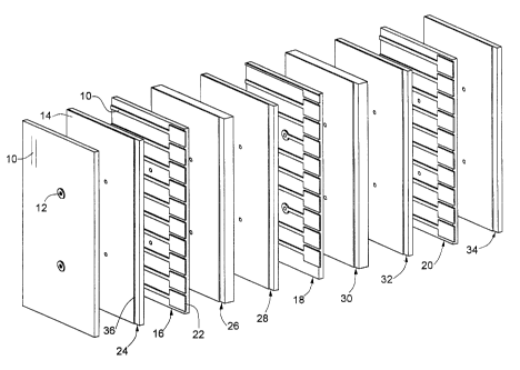
Referring to Figs. 1 and 2 there is shown a
multilayer circuit board constructed in accordance with
the invention. Circuit traces 10 are provided on layer: of
the board and some of which may be connected to others
layers via plated through holes 12. Ground planes 14 may
be provided on. layers adjacent to signal layers to pro~ride
a shielded structure. The multilayer circuit board
structure is itself known and can take a variety of well
known forms and configurations. In accordance with the
invention circuit traces on selected layers of the board
extend to a side surface of the board for direct
connection to contacts of a mating connector, cir.~.uit
board or other device. As seen in Fig. 2, the tracer 10
on layers 16, 18 and 20 terminate in enlarged contact =_:nds
22 which extend beyond the plane of the side of the
circuit board by a small amount, typically .001 inch. xhe
contact ends 22 in the illustrated embodiment are of
greater cross-sectional area than that of the associ,3ted
traces to provide an intended contact area. Th.e con~:act
CA 02293956 2000-O1-OS
_g_
ends may be plated with gold or plated or coated with
other appropriate conductive material to enhance contact
performance by improving conductivity or preventznc~ or
minimizing oxidation or corrosion of the contact er..ds.
Contact pads can be attached or provided on the co°~tact
ends as shown in Fig. 1A. These pads may be of co:_~per,
conductive epoxy or other conductive material and may be
deposited on yr attached to the respective ends of the
tracers.
0 Zt is emphasized that the contact areas of the
circuit board are only the end areas of the assoc:.ated
tzaces, such as contacts 22 which are generally orthogonal
to the plane of the circuit board. The surfaces of the
traces which terminate in contacts 22, which are coplanar
with the plane of the board are not employed to conta ct a
mating connector.
Ground planes can be provided on selected k~~ard
layers to provide shielding. As seen in Fig. 2 a gm~und
plane 14 is provided on a surface of layers 24 and 26 on
respective sides of signal layer 16. Ground planes are
also provided on layers 28 and 30 on respective sides of
layer 18, and ground planes are provided on layers 32 and
34 on respective sides of layer 20. Various oc=her
shielding arrangements can be provided as well known in
the art . The ground plane extends to an edge 36 on Each
layer which is inward of the outer edge or side of the
circuit board from which the contacts 22 extend. The
recessed ground plane edges prevent shorting by cont=_~cts
mating with the ends 22. The ground plane is recesse~7. by
a small amount, typically 15 thousands of an inch.
Alternatively the ground plane can extend to the
outer side of the circuit board and with the exposed =_:dge
of the ground plane insulated with an appropriate coaxing
to px-event short circuiting of mating contacts.
A greatly enlarged edge or end view of a multil;ayer
circuit board is shown in Fig. 4 A row of signal cont;~cts
CA 02293956 2000-11-O1
-6-
40 are provided in alternate Layers 42, 44 and 46. A row
of ground contacts 48 are provided in layers 50 and 52
which are adjacent the assocs_ated signal layers. Ground
planes 54 are provided on surfaces of the layers as
illustrated such that the signal contacts and associated
signal traces are shielded by outer ground planes. The
ground planes are selectively connected to the ground
contacts 48 for connection to a ground terminal of
equipment to which the circuit board is connected.
In a typical multil.ayer_ board, the overall board
thickness can vary from about .062 to .125 inch. For an
eleven layer board, a typical thickness is about .125
inch.
Interconnection to the ~>ide contacts is provided by
mating contacts which rest>ectively engage the contact ends
of the side of the board. The mating contacts are
preferably resilient conductive columns having contact
ends which are maintained =Ln engagement with the contact
ends of the board. Deferring to Fig 5, there is shown a
cutaway enlarged view of contact ends 60 engaging the
contacts of the resilient columns 62 of a contact assembly
64. The opposite contact's of the resilient columns are in
engagement with respective contact areas 66 of a circuit
board 68.
Referring to Fig. 6 a contact assembly is shown which
includes a thin supporting sheet 70 of insulating material
having a plurality of resi:Lient conductive columns 72
supported in openings provi.de~d in sheet 70. The columns
72 each have respective contact ends 74. The columns are
fabricated in one embodiment of conductive e:Lastomeric
material and have a central. section of reduced cross-
section for retaining the columns in the mounting openings
of sheet 70, as shown in enlarged form in Fig. 7.
The columns are preferably of oval configuration
having a longer axis along the axis of a row of contact
ends to be engaged. The oval configuration
CA 02293956 2000-O1-OS
_7_
provides an enhanced contact area with the contact en;is of
the circuit board. other contact configurations can be
employed to suit particular requirements or
specifications.
In an alternative embodiment, the contact ends 6; are
supported on a substrate material 61 which typically is
the material which constitutes a cixcuit board layer, as
shown in Fig. 8.
The side interconnect in accordance with the
invention is particularly useful in prov:.ding
interconnection between daughter boards and a back~>lane
such as widely used in the computer and telecommunicai:ions
industries. For such an interconnection, the contact
assembly of conductive resilient elements is interx~osed
between the contact side of a circuit board and m~.ting
contacts of a backplane, as illustrated in Fig. 9.
Interconnection is provided between the side contact=_; of
the daughter boards) 80 and corresponding contacts of the
backplane B2. A plurality of such daughter boards can be
2o arranged in parallel disposition on a common backpla-re.
The daughter board can be maintained in engagement with
the contact assembly and backplane by suitable retention
hardware.
The invention also finds application in a board to
board interconnection as shown in Fig. 10. A printed
circuit board 90 is interconnected to a spaced cir::uit
board 92 by an interconnecting circuit board 94 hacTing
side interconnects as described above. A pair of
resilient conductive contact assemblies 96 and 98 are
provided at respective sides of interconnect board 9~. to
achieve resilient compressive interconnection between the
contact ends of board 94 arid respective contacts of
circuit boards 90 and 92.
The retention hardware can include elements for
maintaining the alignment of the contact ends of the
circuit board and the conductive columns of the contract
CA 02293956 2000-O1-OS
assembly and mating contacts of a backpZane or other
interconnection device. The contact assembly can it: self
have alignment elements to maintain proper contact
alignment.
The invention is not to be limited by what has been
particularly shown and described as alternatives may :occur
to those of skill in the art without departing ~ron~ the
spirit and true scope of the invention as set forth i» the
claims.