Note: Descriptions are shown in the official language in which they were submitted.
CA 02294026 1999-12-10
WO 98/57252 PCT/US98/11889
PROGRAMMABLE LOGIC DATAPATII THAT MAY BE USED IN A
FIELD PROGRAMMABLE DEVICE
BACKGROUND OF THE INVENTION
Field of the invention:
The invention relates to the field of logic devices. More specifically, the
invention relates to the field of programmable logic devices.
Background information:
One of the core functional units of a computer processor (or CPU) is the
arithmetic/logic datapath, or simply, the datapath. The datapath is typically
responsible for executing various arithmetic and/or logic operations supported
by
the instruction set architecture (ISA) of a computer system. As such, the
datapath
typically includes an arithmetic logic unit (ALU) that performs
arithmetic/logic
operations, an address generation unit to provide memory addresses, and a
control
unit to provide the proper control signals for the various devices of the
datapath to
perform the desired operation(s).
The control signals that control the operations of the datapath may be
considered as a vector of bits, which is known as a "direct control vector",
since it
directly controls the datapath operations. The width of this direct control
vector
varies greatly in CPU designs, and both the overall width as well as the
meaning of
the individual control bits is dependent on detailed aspects of the design.
However,
for typical CPU designs, the width of the direct control vector is from about
50 to
150 bits. Typically, the direct control vector is developed from a combination
of
bits in the instruction, processor state bits (which are sometimes known as
"mode
bits"), and logic gates. The combination of instruction bits and mode bits,
all of
which may change on each cycle, can be considered as an "indirect control
vector"
since it indirectly controls the datapath operations. The indirect control
vector is
normally much less wide than the direct control vector, about 10 to 30 bits in
a
typical CPU design. For example, when an ADD instruction is issued in a CPU,
an
opcode (the indirect control vector] that is contained in the ADD instruction
is
decoded by the control mechanism to generate appropriate control signals (the
direct
control vector) to cause the ALU to add the two operands indicated by the ADD
1
CA 02294026 1999-12-10
WO 98/57252 PCT/US98/11889
instruction. In a similar manner, other relatively simple arithmetic and/or
(Boolean)
logic operations may be realized by the datapath of the CPU.
Several aspects of a CPU's datapath may be limited by various device
and/or design constraints. For example, operands in a CPU datapath are
typically
limited to those of fixed length to simplify the datapath and control
mechanisms of
the datapath, which in turn, may result in improved system
performance/efficiency.
Similarly, some CPU designs, such as those implemented in reduced instruction
set
architecture (RISC) processors, increase performance by limiting the
complexity
and number of types of operations supported by the datapath to minimize
control
signals, minimize/simplify the number of datapath components, etc.
A CPU's ISA cannot create more direct control vectors than 2x, where X is
the width in bits of the indirect control vectors. This is because every
possible
direct control vector corresponds to a distinct indirect control vector, so
even though
there may be more bits in the direct control vector, the number of states
reachable by
the datapath is determined by the indirect control vector. For this reason, a
CPU
design cannot specify in a single instruction all the complex logic operations
that
may be necessary for some applications. Instead, complex logic operations are
broken down into a sequence of simpler ones. In this way, a CPU may perform an
arbitrarily complex logic operation, but it may take many instruction cycles
to
complete.
Some applications require relatively complex logic operations to be
performed at high speed. For example, an application might require a certain
complex logic operation to be performed I million times per second. For a CPU
to
perform these operations in time, it must be able to process instructions at a
still
higher rate. For example, if an operation required 800 instructions on a
certain
CPU, it would have to process 800 million instructions per second to meet the
requirements of the application. In many cases, this is not an economical way
to
implement demanding applications, while in others it is not possible at all.
In such
cases, other devices may be used in place of or in combination with a CPU's
ALU.
For example, programmable logic arrays (PLAs), field programmable gate arrays
(FPGAs), and application specific integrated circuits (ASICs) may be tightly
coupled to serve as coprocessors to a CPU. The coprocessor elements, whether
2
CA 02294026 1999-12-10
WO 98/57252 PCT/US98/11889
ASICs, PLAs, or FPGAs, are configured to perform the complex logic operations
required by the application in a much more parallel manner than a CPU, so that
the
operations can be done at a lower, and more economical, clock rate.
While ASICs are specifically designed state machines and datapaths, PLAs
and FPGAs typically contain an array/matrix of logic circuits (e.g., logic
gates,
memory cells, etc.) in which connections between particular logic circuits may
be
programmed after manufacture (e.g., by a user in the field; hence, the term
"field"
programmable). As such, PLAs and FPGAs may be configured to perform
relatively complex logic operations by making the proper pattern of
interconnections
(e.g., by burning in fuses or programming individual SRAM cells) in the logic
array of such devices. Often, this is analogous to defining a single, highly
specialized CPU instruction specifically for the application, or in more
complex
cases a better analogy might be to defining a highly specialized datapath that
implements several specialized instructions using its own direct and indirect
control
vectors, which may be supplied by the CPU.
However, PLAs, FPGAs and ASICs suffer from some limitations. For
example, ASICs cannot be reprogrammed. As another example, certain PLAs and
FPGAs cannot be reprogrammed once configured and installed (often referred to
as
"one-time programmable"). Thus, such devices may not be suitable for
applications
wherein the execution of various logic operations may be required.
Furthermore, a
substantial portion of circuitry in PLAs and FPGAs may be unused, resulting in
power and/or cost inefficiency.
Although some FPGAs may be re-programmed to support various logic
operations and numbers of inputs, such devices also suffer from limitations.
For
example, in an SRAM cell-based FPGA, the interconnection array in which the
various configurable logic blocks (CLBs) reside is typically programmed by
pass
transistors, which may result in relatively large "on" resistance.
Furthermore,
interconnect delays in SRAM cell-based FPGAs may be relatively large due to
certain wires of unpredictably varying, and sometimes relatively long, length.
Yet
further inefficiency may be caused by the presence of multiple wires in the
interconnect array which may be unused, resulting in increased capacitive load
and
increased device driver power requirements; and by the need for multiple pass
transistors and SRAM cells to complete each logical connection. Finally, the
3
CA 02294026 1999-12-10
WO 98/57252 PCT/US98/11889
number of control/configuration bits typically required to program an FPGA
(e.g.,
produce the appropriate interconnections between the CLBs) may exceed 250,000
bits, making dynamic (e.g., "on the fly"; on a cycle-by-cycle basis) re-
configuration/re-programming relatively difficult and commercially
impractical.
SUMMARY OF THE INVENTION
A method and apparatus for providing a programmable logic datapath that
may be used in a field programmable device is described. According to one
aspect
of the invention, a programmable logic datapath is provided that includes a
plurality
of logic elements to perform various (Boolean) logic operations from operand
bits
that may be furnished from operand register banks, inputs to the field
programmable device, results of previous operations, and so forth. The
programmable logic datapath further includes circuitry to dynamically select,
route
and combine operand bits between the plurality of logic elements. In one
embodiment, by providing control bits concurrently with operand bits to
selecting,
routing and combining circuitry, the programmable logic datapath of the
invention
can provide dynamic programmability on a cycle-by-cycle basis to perform a
number of logic operations on inputs of various lengths and outputs.
According to another aspect of the invention, a field programmable device
containing the programmable logic datapath, as well as additional circuitry
for
operating the programmable logic datapath, is provided. In one embodiment, the
field programmable device includes circuitry for decoding indirect control
vectors
into direct control vectors that specify the operations) to be performed by
the
programmable logic datapath on a cycle by cycle basis.
According to another aspect of the invention, a field programmable device
containing the programmable logic datapath contains additional datapath
circuitry
specialized for performing arithmetic operations.
According to a still further aspect of the invention, one or more field
programmable devices containing some or all of these elements may be
integrated
onto a single semiconductor chip together with other system elements,
including
CPUs, specialized I/O circuits, FPGA circuits, and so on.
The programmable logic datapath overcomes many limitations of the prior
art. Although a useful embodiment of it will require a much wider direct
control
vector than a CPU datapath, the programmable logic datapath can perform many
4
CA 02294026 1999-12-10
WO 98/57252 PCT/US98/11889
complex logic operations in a single cycle that are well beyond the capability
of a
CPU datapath. Thus, for certain applications, it is more comparable to an ASIC
or
FPGA. However, the ASIC is not field programmable. Compared to an FPGA,
the programmable logic datapath will require significantly fewer control bits
for a
given complexity of logic operations. Partly for this reason, it becomes
practical to
change the direct control vector on every cycle, which increases flexibility.
Finally,
because the programmable logic datapath uses predefined connections, with
selecting and routing performed by multiplexers, the speed of interconnection
paths
is increased while the unpredictability of this speed is greatly decreased.
BRIEF DESCRIPTION OF THE DRAWINGS
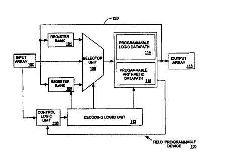
Figure 1 is a block diagram illustrating a field programmable device
according to one embodiment of the invention;
Figure 2 is a more detailed block diagram of the programmable logic
datapath section of the field programmable device according to one embodiment
of
the invention;
Figure 3A is a block diagram illustrating the rearrangements of three bit
fields according to one embodiment of the invention;
Figure 3B is a block diagram illustrating one group of three multiplexers that
selectively provides one of the three bit fields according to one embodiment
of the
invention;
Figure 4 is a block diagram illustrating a reduction network in the
programmable logic datapath according to one embodiment of the invention;
Figure SA is a schematic diagram illustrating the subset selection circuit 402
and the level one logic circuit 404 of Figure 4 according to one embodiment of
the
invention;
Figure SB is a schematic diagram illustrating an accumulator-based bit
generation circuit 40 located in the alignment circuit 406 of Figure 4
according to
one embodiment of the invention;
Figure SC is a schematic diagram illustrating the remainder of the alignment
circuit 406 of Figure 4 according to one embodiment of the invention;
CA 02294026 1999-12-10
WO 98!57252 PCT/US98/I 1889
Figure SD is a data flow diagram illustrating a 4x4 matrix transposition of
operands between four adjacent reduction networks according to one embodiment
of the invention;
Figure SE is a data flow diagram illustrating a 2x2 matrix transposition of
operands between four adjacent reduction networks according to one embodiment
of the invention;
Figure SF is a schematic diagram illustrating the level two logic circuit 412
and the output selection circuit 414 of Figure 4 according to one embodiment
of the
invention;
Figure 6 is a diagram illustrating an output array according to one
embodiment of the invention;
Figure 7A is a block diagram illustrating an exemplary programmable
system chip 700 according to one embodiment of the invention; and
Figure 7B is a block diagram illustrating an exemplary computer system
including a programmable peripheral device 730 according to one embodiment of
the invention.
DETAILED DESCRIPTION
In the following description, numerous specific details are set forth to
provide a thorough understanding of the invention. However, it is understood
that
the invention may be practiced without these specific details. In other
instances,
well-known circuits, structures and techniques have not been shown in detail
to
avoid obscuring the invention.
AN EMBODIMENT OF THE FIELD PROGRAMMABLE DEVICE
Figure 1 is a block diagram illustrating a field programmable device
according to one embodiment of the invention. In Figure 1, a field
programmable
device 100 is shown which includes an input array 102 and an output array 118.
The input array 102 represents one or more bits that are input to the field
programmable device 100. Similarly, the output array I 18 represents one or
more
bits that are output by the field programmable device 100. In one embodiment,
the
input array 102 and/or the output array 118 may represent registered/latched
input
and output bits, respectively.
6
CA 02294026 1999-12-10
WO 98/57252 PCT/US98/11889
The input array 102, a register bank 104, and a register bank 106 are shown
coupled to a selector unit 108. The register banks 104 and 106 each represents
a set
of one or more registers/latches for storing data (or a subset thereof): 1 )
input into
the input array 102; and/or 2) output by the datapath(s) provided via a
feedback path
120. Thus, the register bank 104 andlor 106 may represent or include an
accumulator, as will become further apparent from the description that
follows. In
one embodiment, the register banks 104 and 106 are 32-bits wide and 256 bits
deep, and are dual ported for read operations and single ported for write
operations.
In alternative embodiments, more or fewer register banks may be used having
various port and storage capacity configurations. For example, one embodiment
has no register banks, but stores inputs and/or results needed for subsequent
datapath operations in registers contained in the datapath. Another embodiment
does not include any mechanism (e.g., register banks) to store inputs and/or
outputs
for use in subsequent datapath operations.
The selector unit 108 is shown coupled to provide input from the register
bank 104, the register bank 106, and/or the input array 102 to a programmable
logic
datapath 114 and/or a programmable arithmetic datapath 116. The programmable
logic datapath 114 and the programmable arithmetic datapath 116 are both
further
coupled to provide the output data to the output array 118. The programmable
logic
datapath 114 and the programmable arithmetic datapath 116 are configured to
perform (Boolean) logic operations and arithmetic (e.g., add, multiply,
divide, etc.)
operations, respectively.
In Figure 1, the input array 102 is further coupled to a control logic unit
110, which in turn is coupled to a decoding logic unit 112. In one embodiment,
the
control logic unit 110 provides an indirect control vector (ICV) to the
decoding logic
unit 112. While any number of ICVs may be stored in the control logic unit
110, in
one embodiment of the invention the control logic unit 110 stores 128 ICVs,
each
102 bits in length and consisting of several sub-fields of differing lengths.
Some of
these sub-fields are used directly to control parts of the field programmable
device
100, and are therefore called "direct ICV sub-fields". Other of these sub-
fields are
further decoded by the decoding logic unit 112, to select other parts of a
direct
control vector (DCV) to program/configure various portions of the field
programmable device 100. These sub-fields are called "indirect ICV sub-
fields".
7
CA 02294026 1999-12-10
WO 98/57252 PCT/US98/11889
The DCV is selected from as many memories as there are indirect ICV sub-
fields. Each memory is of an appropriate width to control those parts of the
field
programmable device 100 to which it is dedicated, and has a depth, or number
of
elements, equal to 2X where X is the length of the indirect ICV sub-field that
addresses that memory. These DCV memories may be of any type, including one
or more of DRAM, SRAM, ROM, etc. While one embodiment is described which
uses subfields and separate memories, alternative embodiments could use most
or
all of the ICV to address a single memory.
In one embodiment, the decoding logic unit stores 16 DCVs for the subset
selection portion (described later herein) of the programmable logic datapath
114 in
a random access memory (RAM) and 16 DCVs in a ROM. The memory width
needed to control this portion of the programmable logic datapath in this
embodiment is 1536 bits, while the length of the indirect ICV sub-field that
addresses this memory is 5 bits. Other memories control other portions of the
selected DCV, applying them as control signals to the selector unit 108, the
register
bank 106, the register bank 104, other parts of the programmable logic
datapath
114, and/or the programmable arithmetic datapath 116. In one embodiment, the
total DCV length when all the fields are accounted for is 2669 bits.
In one embodiment, the field programmable device includes 72 input pins
and 72 output pins. Of the 72 input pins, 64 are used for data and 8 are used
as
interrupt pins directly coupled to the control logic unit 110. Of the 72
output pins,
64 are used for data and 8 are used as output control pins that are set by
dedicated
control fields within the field programmable device.
In one embodiment, the indirect control vectors are selected by the control
logic unit 110 from multiple conceptually distinct "threads" of control, using
parallel
hardware to perform the "thread switching" on a cycle-by-cycle basis. Distinct
portions of the register bank 104 and/or the register bank 106 may be used by
different threads to avoid thread switching overhead. In an alternative
embodiment,
the control logic unit 110 is not present and the decoding logic unit 112 is
operatively coupled to receive the indirect control vectors from the input
array 102
(e.g., an opcode contained in an instruction provided by a microprocessor that
may
be coupled to the field programmable device 100). In yet another alternative
8
CA 02294026 1999-12-10
WO 98/57252 PCT/US98/11889
embodiment, rather than decoding, a serially programmable 1-deep memory is
included to provide the control signals.
Thus, in one embodiment further described herein, by providing
approximately 2,500 control bits concurrently with up to 64 operand bits to
selecting, routing and combining circuitry, the programmable logic datapath of
the
invention can provide dynamic programmability on a cycle-by-cycle basis to
perform a number of logic operations on inputs of various lengths and provide
up to
64 outputs. While an embodiment is described with reference to a specific
number
of inputs, outputs and control bits, alternative embodiments can have more or
fewer
inputs, outputs and/or control bits.
AN EMBODIMENT OF THE LOGIC DATAPATH
Referring to Figure 2, a more detailed block diagram of the programmable
logic datapath section of an field programmable device 100 according to one
embodiment of the invention is shown. In Figure 2, the programmable logic
datapath 114 of Figure 1 is shown coupled to the decoding logic unit 112. As
described with reference to Figure 1, the decoding logic unit 112 provides
control
bits for the various circuits of the field programmable device 100.
REARRANGEMENT
As shown in Figure 2, the programmable logic datapath includes a
rearrangement circuit 202 configured to allow for flexible rearrangement and
duplication of the input data bits. While any number of input bits may be
used, the
embodiment shown receives 48 input bits, which are either the upper 48 or
lower
48 of the 64 bits formed by the concatenation of two 32-bit register bank
outputs. .
The set of input bits may include data bits for a current cycle of operation
and/or
accumulated bits (e.g., output bits from a previous cycle of a logic and/or
arithmetic
operation).
The number of bits output by the rearrangement circuit 202 is a design
choice. Thus, while one embodiment is described that outputs the same number
of
bits as are input, alternative embodiments can output more or fewer bits than
are
input. (If more bits are output than input, by necessity some input bits will
be
duplicated in the output.)
9
CA 02294026 1999-12-10
WO 98/57252 PCT/US98/11889
In one embodiment that receives 48 input bits and provides 48 outputs, the
rearrangement circuit 202 comprises a set of forty-eight 48-to-1 multiplexing
circuits (each coupled to receive the 48 input bits) for selectively routing
any of the
48 input bits to its output. To control the forty-eight multiplexing circuits,
each
multiplexing circuit receives a different set of six control/configuration
bits from the
decoding logic unit 112 (making a total of 288 control bits). Thus, the 48
multiplexing circuits operate to dynamically select and/or rearrange (i.e.,
modify
relative bit positions) the input bits.
In alternative embodiments, the bits input to the rearrangement circuit 202
may be selectively routed to the outputs in fixed sized, non-overlapping
fields of
multiple, consecutive bits. For example, one such embodiment selectively
routes
48 inputs to 48 outputs using 3-bit fields as shown in Figure 3A. This
embodiment
can be implemented using forty-eight 16-to-1 multiplexers, where the forty-
eight
16-to-1 multiplexers are grouped in sets of 3 to create 16 groups of 3
multiplexers.
Figure 3B is a block diagram illustrating one group of 3 multiplexers used to
route
one 3-bit field according to one embodiment of the invention. Each group of
multiplexers receives a different set of 4 control bits provided by the
decoding Logic
unit 112 (the multiplexers in each group each receive the same 4 control
bits).
In general, given J input bits, L output bits, and a rearrangement field size
of F bits (where J/F is an integer), the rearrangement circuit 202 can include
L J/F-
to-1 multiplexing circuits, each controlled by X control signals, where X is
the least
power of 2 greater than or equal to J/F, and such that consecutive groups of F
multiplexing circuits are controlled by the same X control signals. To
illustrate, in
the embodiment described above that uses forty-eight 48-to-1 multiplexers,
J=48,
L=48, F=1, and X=6; while, in the embodiment described above that uses forty-
eight 16-to-1 multiplexers, J =48, L=48, F=3, and X=4. While two embodiments
of the rearrangement circuit 202 have been described, it should be understood
that
the rearrangement circuit 202 could be adapted for various input and
rearrangement
bit field widths.
SELECTIVE FIELD NEGATION
As shown in the embodiment illustrated in Figure 2, the rearrangement
circuit 202 is followed by a selective field negation circuit 210. The
selective field
CA 02294026 1999-12-10
WO 98157252 PCT/US98/11889
negation circuit 210 selectively negates certain bits output by the
rearrangement
circuit 202 based on control bits provided by the decoding logic unit 112. In
one
embodiment, the selective field negation circuit 210 includes one or more
logic
elements that are configured to selectively negate alternating fields output
by the
rearrangement circuit 202. The field width used for the selective field
negation
circuit may be unrelated to that used by the rearrangement circuit. As shown
in
Figure 2, the selective field negation circuit 210 includes a series of
exclusive-OR
(XOR) gates positioned to accept some of the bits output by the rearrangement
circuit 202. In one embodiment, the field width for the selective field
negation
circuit is 3, which means that alternating groups of 3 bits output by the
rearrangement circuit 202 are either wired straight through or input to an XOR
gate.
By supplying a control bit from the decoding logic unit to the other input of
each of
the XOR gates, the selective field negation circuit 210 provides for the
selective
negation of every other field output by the rearrangement circuit 202. The
number
of distinct control bits may be varied according to the degree of general
purpose
control required. In one embodiment, a different control bit is used for each
field of
3 XOR gates, so that the total number of control bits is 8 (since there are
sixteen 3-
bit fields from 48 bits and half of them are wired straight through).In
another
embodiment, one bit fields are used wherein every other output of the
rearrangement circuit is coupled as an input to an XOR gate, and there are a
total of
24 control bits used.
By using a multi-input negation element (e.g., an XOR gate) and by
allowing input of an appropriate control input to the negation element,
negation of
(alternating) rearranged fields may be performed in a controlled/selective
manner.
As such, subsequent stages of the programmable logic datapath 114 described
below can implement logic operations upon mostly positive and/or negative
terms, a
relatively balanced combination of positive and negative terms, and/or via
logical
equivalencies as provided by DeMorgan's Law over mostly positive or negative
terms.
While one embodiment has been described that selectively rearranges
according to predetermined bit fields and selectively negates alternating bit
fields,
alternative embodiments of the invention may not rearrange input bits and/or
not
include a selective field negation circuit. Furthermore, in alternative
embodiments,
11
CA 02294026 1999-12-10
WO 98/57252 PCT/US98/11889
input bit field rearrangement and/or negation may be performed according to
several
methods other than the ones described above. For example, selective negation
may
be performed using logic elements other than XOR gates (e.g., inverters and
multiplexers).
REDUCTION NETWORK BANK
Referring again to Figure 2, the negated and/or non-negated results of the
rearrangement circuit 202 (having a total width of 48 bits in one embodiment)
are
provided to a reduction network bank 212. The reduction network bank 212
comprises a set of (k) reduction networks shown in Figure 2 as the elements
RN1
through RNk. The number of reduction networks is a design choice. In one
embodiment, each of 32 reduction networks in the reduction network bank 212
receives the negated and/or non-negated outputs from the rearrangement circuit
202
and generates a two bit result. The structure and operation of a reduction
network
according to one embodiment of the invention will be described in further
detail
below with reference to Figures SA-SF.
POST PROCESSING
The reduction network bank 212, upon performing various bit routing, bit
selection, and/or logic operations, outputs 64 bits to a post processing unit
214.
The post processing unit 214 may be configured to perform various functions
upon
the output of the reduction network bank 212. For example, in one embodiment,
the post processing unit 214 may be configured to detect the number and/or
positions of (e.g., zeros and/or ones) in various fields of the output bits of
the
reduction network bank 212. Several exemplary functions that may be performed
by post processing unit 214 and/or the reduction network bank 212 are
described
below.
In alternative embodiments, the post processing unit 214 may not be
included in the programmable logic datapath 114. For example, in one
embodiment, a device (e.g., a processor) coupled to the programmable logic
datapath of the present invention obtains the output/result generated by the
12
CA 02294026 1999-12-10
WO 98/57252 PCT/US98/11889
programmable logic datapath and performs a "post processing" function. In
another
embodiment, post processing functions are not performed.
AN EMBODIMENT OF A REDUCTION NETWORK IN THE REDUCTION NETWORK
BANK
Figure 4 is a block diagram illustrating one reduction network 400 in the
reduction network bank 212 according to one embodiment of the invention. The
reduction network 400 includes a subset selection circuit 402. In the
embodiment in
which the rearrangement circuit provides 48 outputs, the subset selection
circuit 402
is configured to receive the 48 outputs from the rearrangement circuit 202
and/or the
selective field negation circuit 210. The subset selection circuit 402
provides
outputs to a level one logic circuit 404.
SUBSET SELECTION
Figure SA is a schematic diagram illustrating the subset selection circuit 402
and the level one logic circuit 404 of Figure 4 according to one embodiment of
the
invention. In Figure SA, the circuitry above and below the dashed line 500 is
respectively part of the subset selection circuit 402 and the level one logic
circuit
404.
In Figure SA, an embodiment of the subset selection circuit 402 that
includes four groups of NAND and AND gates is shown, wherein each of the four
groups includes twelve pairs of NAND and AND gates. Each AND gate is coupled
to receive a control bit C[i,j] and an input bit Rn, where i indicates one of
the 32
reduction networks 0-31, j represents one of the 48 gate control bits 0-47,
and Rn
represents one of the bits 0-47 input to the reduction network. Each NAND gate
receives the same inputs as the AND gate to which it is paired, except the Rn
input
to the NAND gate is negated.
By gating the 48 bits with a control bit, a subset of the input bits can be
selected (e.g., when the control bit is a logical "1 ", the input bit will be
contained in
a subset). The result generated by the 48 NAND gates of the subset selection
circuit
402 is shown in Figure SA as four twelve-bit output lines ZI-Z4. Similarly,
the
result of the 48 AND gates is shown as four twelve-bit output lines S I-S4. It
13
1
CA 02294026 1999-12-10
WO 98!57252 PCT/US98/11889
should be understood, however, that each of the four lines S 1-S4 and Zl-Z4
represents twelve logically/electrically distinct bits.
While one embodiment has been described wherein subset selection is
implemented with a series of NAND and AND gate pairs, alternative embodiments
may use several other types and/or combinations of logic elements (e.g., NAND
gates, NOR gates, MUXes, etc.) to perform subset selection. For example,
commonly available logic synthesis tools, such as Design Compiler~ from
Synopsys0, Inc., might be applied to a design description of the subset
selection to
create the logically equivalent configuration of gate elements that is optimal
for a
given VLSI design environment. Furthermore, alternative embodiments of the
reduction network 400 may not include a subset selection circuit.
LEVEL ONE LOGIC
The result generated by the subset selection circuit 402, and in particular,
the
twelve-bit output lines Z1-Z4 and S 1-S4, are shown coupled to four groups of
logic
circuits A-D, wherein each group includes an AND, OR, and XOR logic network.
The four output lines Z1-Z4 are respectively coupled to the AND logic of logic
groups A-D, while the four output lines Sl-S4 are respectively coupled to both
the
OR and XOR logic of logic groups A-D. Although each of the four groups of
logic
circuits A-D is conceptually shown to include three 12-input logic elements,
in
practice, it should be understood that such elements typically have fan-in
limitations
that may limit the number of inputs. Accordingly, in one implementation, each
group of the logic circuits A-D may contain twelve 2-input AND gates, twelve 2-
input OR gates, and twelve 2-input XOR gates. However, it should be understood
that several other combinations of input-type (e.g., 2-input, 4-input, 8-
input) and/or
logic type (e.g., NAND, NOR, NOT, etc.) of logic elements may be utilized in
alternative embodiments of the level one logic circuit 404. While one
embodiment
is shown having three different logic functions in each logic circuit group A-
D,
alternative embodiment may support more, less, and/or different logic
functions.
As shown in Figure SA, each of the four logic circuit groups A-D generates
three one-bit outputs. For example. the logic circuit group A is shown to
generate
an AND output bit Al, an OR output bit A2, and an XOR output bit A3.
Similarly,
14
CA 02294026 1999-12-10 p~TNS 9a ~ 1
IPEAIUS 16 APR 1999
the logic circuit groups B, C, and D are shown to generate three output bits B
1-B3,
C1-C3, and D1-D3, respectively.
While one embodiment is shown in which static logic is used in the logic
levels, alternative embodiment replace certain or all of the static logic with
logic
blocks (e.g., SRAMs).
ALIGNMENT
Referring back to Figure 4, the level one logic circuit 404 is shown further
coupled to an alignment circuit 406. The alignment circuit 406, according to
one
embodiment of the invention, is described with reference to Figures SB and SC.
In one embodiment of the invention, the alignment circuit 406 is configured
to receive the output bits A1-D3 of the level one logic circuit 404, as well
as a set of
accumulator-based bits, as shown in Figure SC. Figure SB will now be described
to illustrate the generation of the accumulator-based bits, according to one
embodiment of the invention.
Accumulator
Figure SB is a schematic diagram illustrating an accumulator-based bit
generation circuit 40 located in the alignment circuit 406 of Figure 4
according to
one embodiment of the invention. As shown in Figure SB, the accumulator-based
bit generation circuit 40 includes a set of selectors 502, 504, 506, and 508.
Each
selector is coupled to receive an accumulator register bit, depicted as ACC
REG
BIT. The ACC REG BITS constitute an additional input to the programmable logic
datapath component of the field programmable device, which may represent a
stored
'-' result of one or more logic and/or arithmetic operations previously
performed by the
field programmable device 100 of Figure 1, or could alternatively be furnished
as an
additional output of selector unit 108. In one embodiment, there are 64 ACC
REG
BITs stored within the programmable logic datapath, two for each reduction
network 400 of Figure 4, with one bit associated with selectors 502 and 504
and the
other associated with selectors 506 and 508. In addition to the appropriate
ACC
REG BIT, each selector receives the result of gating the ACC REG BIT with one
of
the output bits A1-D3 of level one logic circuit 404 (e.g., through an AND,
OR,
and XOR logic circuit, as depicted in Figure SB). In particular, since the
output bit
A 1 was generated by an AND operation, the output bit A 1 and the appropriate
ACC
AMENDED SHEET
CA 02294026 1999-12-10
WO 98/57252 PCT/US98/11889
REG BIT are provided as inputs to an AND gate. In this manner, the result of a
previous operation (ACC REG BITs) can be logically combined with the current
input.
While one embodiment is shown in which each of the selectors 502, 504,
506, and 508 receives the same two control bits, in an alternative embodiment
of the
invention each selector receives a different set of control bits. The control
bits
provided to each selector facilitates selection of one of the inputs of that
selector,
such as the ACC REG BTT or the gated result of the ACC REG BIT and another bit
(e.g., one of the output bits Al-D3 of the level one logic circuit 404
described with
reference to Figure SA). Accordingly, the selectors 502, 504, 506, and 508
output
a selected one of an ACC-BASED BIT l, ACC-BASED BIT 2, ACC-BASED BIT
3, and ACC-BASED BIT 4, respectively.
It should be appreciated that alternative embodiments may use several types
and combinations of logic elements to gate the ACC REG BIT, or may not gate
the
ACC REG BIT. Furthermore, alternative embodiments of the invention may not
include an accumulator-based bit generation circuit and/or utilize an
accumulator
result.
Alignment Elements
Figure SC is a schematic diagram illustrating the remainder of the alignment
circuit 406 of Figure 4 according to one embodiment of the invention. In
Figure
SC, a set of four alignment elements 510, 512, S 14, and 516 are shown. Each
of
the alignment elements 510, 512, 514, and 516 is coupled to receive an ACC-
BASED BIT and three output bits of one of the logic circuit groups A-D
described
with reference to Figure SA. For example, the alignment element 510 is shown
receiving the ACC-BASED BIT 1, and the bits Al-A3. Similarly, the alignment
element 512 is configured to receive the ACC-BASED BIT 2, and the bits B1-B3.
Each of the alignment elements 510, 512, 514, and 516 also receives two
control bits. While in one embodiment the alignment elements in each reduction
network (e.g., the alignment elements 510, 512, 514, and 516) receive the same
two control bits, the level of individual control of the alignment elements is
a design
choice. In one embodiment, the alignment elements 510, 512, 514, and S 16 are
each configured to rotate their respective four inputs by either 0, 1, 2, or 3
positions, based on the two control bits, and generate three outputs, RA1-RA3,
16
CA 02294026 1999-12-10
WO 98/57252 PCT/US98/11889
RB1-RB3, RCI-RC3, and RD1-RD3, which are grouped as ROT BIT GROUP I,
ROT BIT GROUP 2, ROT BIT GROUP 3, and ROT BIT GROUP 4, respectively
(ROT is an acronym for "rotated"). The three outputs of each of the alignment
elements 510, 512, 514, and 516 represents the rotated/shifted result of three
of the
four inputs to that alignment element. Thus, in one embodiment, the output bit
RA 1
of the alignment element 510, for example, may correspond to one of the ACC
BASED BIT 1, A1, A2, or A3, depending on the rotation of input bits performed
by the alignment element 510.
The alignment elements 510, 512, 514, and 516 are utilized in one
embodiment to route/align data bits as they propagate through levels of logic
in a
reduction network. For example, in the creation of AND-OR logic functions, the
level one logic circuit 404 may perform AND operations and the alignment
circuit
406 may be utilized to align the result of the AND operations to OR logic
elements
(e.g., as may be contained in a level two logic circuit, as described below).
However, it should be understood that alternative embodiments of the
invention may not include an alignment circuit. It should further be
understood that
there are several alternative embodiments of the alignment circuit 406 and the
alignment elements 510, 512, 514, and S 16. For example, shifters,
multiplexers,
and/or other devices may be utilized to implement the alignment elements 510,
512,
514, and 516. Furthermore, in alternative embodiments, each alignment element
may be configured to receive/generate fewer or greater than the number of
inputs,
control signals, and/or outputs as described with reference to the exemplary
embodiment of alignment elements illustrated in Figure SC. For example, in one
embodiment, one or more alignment elements of the alignment circuit 406 does
not
receive an ACC-BASED BIT.
OPTIONAL NEGATION
Referring back to Figure 4, the alignment circuit 406 is further coupled to an
optional negation circuit 408. In one embodiment, the optional negation
circuit
seiectivelv negates one or more of the outputs ROT BIT GROUP l, ROT BIT
GROUP 2. ROT BIT GROUP 3, and ROT BIT GROUP 4 generated by the
alignment circuit 406. In one embodiment, the optional negation circuit
contains a
set of controlled negation elements (e.g., XOR gates) to selectively negate
the
17
CA 02294026 1999-12-10
WO 98/57252 PCT/US98/11889
output bits RA1-RA3, RB1-RB3, RC1-RC3, and RD1-RD3 generated by the
alignment circuit 406 based on a control bit. While one embodiment is
described in
which the output bits of the alignment circuit 406 are selectively negated as
a single
group, the level of individual control of the negation elements is a design
choice
(i.e., additional control bits could be used to selective negate different
sets of the
bits output by the alignment circuit 406).
The optional negation circuit 408 may be utilized in an embodiment of the
invention to facilitate certain logic functions, for example, through
DeMorgan's
law. It should be understood, however, that alternative embodiments of the
reduction network 400 may not include the optional negation circuit 408.
TRANSPOSITION
Referring again to Figure 4, the bits output by the optional negation circuit
(ROT BIT GROUPS 1-4, one or more of which may be negated) are provided to a
transposition circuit 410. In one embodiment, the transposition circuit 410
includes
a set of multiplexers configured to accept input, such the ROT BIT GROUPS 1-4,
from a set of reduction networks in the reduction network bank 212. The set of
multiplexers provide optional transposition (i.e., positional interchange) of
rotate bit
groups between the set of reduction networks in the reduction network bank
212.
In one embodiment, the set of reduction networks whose rotate bit groups may
be
transposed includes adjacent reduction networks of the reduction network bank
212.
Figures SD and SE illustrate two exemplary transposition options that may
each or both be implemented by the transposition circuit 410. Figure SD is a
data
flow diagram illustrating a 4x4 matrix transposition of ROT BIT GROUPs between
four adjacent reduction networks. In Figure SD, the ROT BIT GROUPs 1-4
generated by an alignment circuit, for example, the alignment elements 510,
512,
514, and 516, are depicted by four squares for each of four reduction networks
1,
2, 3, and 4.
As shown by the arrows in Figure SD, the ROT BIT GROUPS of one
reduction network, such as the reduction network 400, may be transposed (
i.e.,
positionally interchanged) with the ROT BIT GROUPs of another reduction
network. For example, as shown in Figure SD, the ROT BIT GROUP 2 of a
18
CA 02294026 1999-12-10 ~~~VV
~PEA/~!S 16 aPR 1999
reduction network 1 (RN 1 ) may be transposed with the ROT BIT GROUP 1 of a
reduction network 2 (RN2) (which may be adjacent to the reduction network 1 in
a
reduction network bank). Similarly, as indicated in Figure SD, the ROT BTT
GROUP 3
of the reduction network 1 (RN 1 ) may be transposed with the ROT BIT GROUP 1
of a
reduction network 3 (RN3), while the ROT BTT GROUP 4 of the reduction network
1
(RN 1 ) may be transposed with the ROT BTT GROUP 1 of the reduction network 4
(RN4). Other transposition options are shown by the arrows in Figure SD.
Figure SE is a data flow diagram illustrating a 2x2 matrix transposition of
ROT
BIT GROUPs between four adjacent reduction networks. As described with
reference
to Figure SD, the ROT BTT GROUPs 1-4 generated by an alignment circuit, such
as the
alignment elements 510, 512, 514, and 516, are also depicted in figure SE by
four
squares for each of four reduction networks 1, 2, 3, and 4. Similarly, arrows
are shown
,,.Y...., in Figure SE to indicate the ROT BIT GROUPs interchanged between the
reduction
networks. For example, as illustrated by one of the arrows in Figure SE, the
ROT BIT
GROUP 3 of the reduction network 1 (RN 1 ) is interchanged with the ROT BTT
GROUP 1 of the reduction network 2 (RN2). (Note: In Figure SE, reduction
networks
1, 2, 3 and 4 are respectively providing rows 1, 3, 2 and 4 of the matrix.)
In a typical embodiment, one or more transpositions patterns would be chosen
to allow positional interchange of ROT BIT GROUPS among a certain number of
reduction networks, and these patterns would be repeated for all the reduction
networks
in the reduction network bank. For example, in an embodiment comprising 32
reduction networks, both 4x4 and 2x2 transposition patterns might be available
for
positional interchange among the 8 groups of 4 reduction networks, where the
first
group consists of {RNI, RN2, RN3, RN4}, the second group consists of {RNS,
RN6,
RN7, RN8 } , and so on.
The number of control bits required depends on the number of transposition
patterns chosen. The input width of the multiplexers required to effect
transposition
depends on both the number of transposition patterns chosen and the position
within the group of reduction networks involved. For example, in an embodiment
with 4x4 and 2x2 transposition patterns, one can refer to Figures SD and SE to
see
how many inputs are needed for each multiplexer. For ROT BIT GROUP 1 of
reduction network 1, no multiplexer is needed, as neither transposition
pattern
interchanges it with another. For ROT BIT GROUP 2 of reduction network l, a 2-
19
AMENDED SHEET
CA 02294026 1999-12-10
WO 98/57252 PCTNS98/11889
input multiplexer is needed as part of the 4x4 transposition network; it will
be
steered by a bit that controls whether the 4x4 transposition is in effect or
not for this
group of 4 reduction networks. For ROT BIT GROUPS 3 and 4 of reduction
network 1, two 2-input multiplexers are needed, one for the 4x4 transposition
and
one for the 2x2 transposition, each steered by a separate control bit. The
pattern is
not the same for the other reduction networks within the group of 4. For
example,
in reduction network 2, ROT BTT GROUP 1 requires two 2-input multiplexers,
while ROT BIT GROUPS 2, 3, and 4 require a single 2-input multiplexer.
While two exemplary transposition options of the transposition circuit of
Figure 4 have been described, alternative embodiments may facilitate
transposition
of operands using several other transposition techniques. For example, the set
of
reduction networks between which transposition may be performed could be fewer
or greater than four, as exemplified in the embodiments shown in Figures SD
and
SE. Furthermore, transposition schemes other than 2x2 matrix and/or 4x4 matrix
may be performed in alternative embodiments. In certain alternative
embodiments,
ROT BIT GROUPs may be transposed within a reduction network. In other
alternative embodiments, the transposition circuit 410 is not included in the
reduction network 400.
While one embodiment is described in which optional negation follows
rotation and in which transposition follows optional negation, alternative
embodiment could rearrange the order of this circuitry. Thus, in an embodiment
having alignment and transposition circuitry, the level two logic described
below is
said to receive data representing the output of the level one logic that has
been
"routed" to the level two logic via alignment and transposition circuitry,
regardless
of the order of the alignment and transposition circuitry.
LEVEL TWO LOGIC
Referring again to Figure 4, the transposed and/or non-transposed ROT BIT
GROUPS are provided by the transposition circuit 410 to a level two logic
circuit
412, which in turn is coupled to an output selection circuit 414. The level
two logic
circuit 412 and the output selection circuit 414, according to one embodiment
of the
invention, are described below with reference to Figure SF.
CA 02294026 1999-12-10
WO 98/57252 PCT/US98/11889
Figure SF is a schematic diagram illustrating the level two logic circuit 412
and the output selection circuit 414 according to one embodiment of the
invention.
In Figure SF, the level two logic circuit 412 and the output selection circuit
414 are
respectively shown above and below the dashed line 550.
In the embodiment depicted in Figure SF, the level two logic circuit 412
comprises a set of logic element types similar to ones included in the level
one logic
circuit 404 described above. As shown, the level two logic circuit 412
includes a
lower term logic 530 and an upper term logic 532, each comprising a two-input
AND, OR, and XOR gate configured to receive adjacent ROT GROUP BTTS. In
one embodiment, each ROT GROUP BIT, such as the bit RA 1 and/or RB 1 shown
coupled to the AND gate of the lower term logic 530, may represent a
transposed
(e.g., from another reduction network) and/or a negated one of the ROT GROUP
BITs. On the other hand, one or more of the inputs to one or more of the AND,
OR, and/or XOR logic elements of the level two logic circuit 412 may directly
correspond (e.g., without transposition and/or negation) to the output of the
alignment elements 510, 512, 514, and 516, described with reference to one
embodiment of the alignment circuit 406.
While one embodiment is described in which the same logic is in both the
level one and two logic circuits, the logic in each level need not be the same
and is a
design choice. Furthermore, while one embodiment is shown have two levels of
logic, alternative embodiments could include additional levels of alignment,
negation, transposition, and/or logic.
OUTPUT SELECTION
The three bits output from the upper term logic 532 of the level two logic
circuit 412 are fed into a selector 524, as well as a fold output selection
circuit 520.
The selector 524, based on two control bits, selects one of the results of the
upper
term logic 532 as an OUTPUT 32. The fold output selection circuit 520 may be
included in every reduction network in the reduction network bank 212 to
"unfold"
the result of the level two logic circuit 412 by one. As such, the fold output
selection circuit 520 of the reduction network 400 receives the same control
bit as
other fold output selection circuits that may be included in other reduction
networks.
Of course, the granularity of control of the folding circuitry is a design
choice.
21
CA 02294026 1999-12-10
WO 98/57252 PCT/US98/11889
As shown in Figure 5F, the three bit result of the fold output selection
circuit 520 are coupled, with corresponding results of the lower term logic
530, to a
fold logic 534 which includes an AND, and OR, and an XOR logic element. In
this
manner, the control bit applied to the fold output selection circuit 520 is
used to
selectively pass the results of the upper term logic 532 to corresponding
gates that
combine the corresponding results of the lower and upper term logic 530 and
532.
While one embodiment of the folding circuitry is described, alternative
embodiments can use different circuitry. For example, an alternative
embodiment
provides a set of two 2-to-1 multiplexors, each of which receives one output
from
the lower term logic 530 and the appropriate logical combination of that
output with
the corresponding output from the upper term logic 532 (e.g., one 2-to-1
multiplexor receives the output of the AND gate in lower term logic 530 and
the
logical AND of that output with the output of the AND gate in the upper term
logic
532).
The results of the fold logic 534 are coupled to a selector 522, which
selects, based on two control bits, one of the results of the fold logic 534
to output
as OUTPUT 0. While distinct control bits are used to control the selectors 522
and
524 in the embodiment shown, the level of individual selection of output is a
design
choice.
In one embodiment, the output of selectors 522 and 524 are respectively
coupled to XOR gates which provide conditional negation of the reduction
network
outputs. These are shown with distinct control bits for each output, however
the
level of individual selection of conditional negation of outputs is a design
choice.
It should be appreciated that alternative embodiments of the invention may
not include fold circuitry (e.g., the fold output selection circuit 520, the
fold logic
534, etc.), the level two logic circuit 412, and/or the selective negation.
OUTPUT
Referring now to Figure 6, a 64 output array 118 according to one
embodiment of the invention is shown. The output array 118 illustrates the
relative
positions of the OUTPUT 0 and OUTPUT 32 result bits generated by the output
selection circuit 414 of a first reduction network (e.g. RN 1 ) of the
reduction
network bank 212. The output array 118 may represent data that is asserted on
one
22
CA 02294026 1999-12-10
WO 98/57252 PCT/US98/11889
or more lines (e.g., on a bus) and/or stored in a storage area, such as a
register,
accumulator, etc.
EXEMPLARY LOGIC OPERATIONS OF AN EMBODIMENT OF THE REDUCTION
NETWORK BANK
In one embodiment, the reduction network bank 212 having 32 reduction
networks receiving 48 selectively rearrangeable/negateable inputs bits may be
utilized to perform one or more of the following exemplary logic operations:
1. 32 1-level functions of 1 to 48 inputs over Boolean AND, OR, XOR
or their negations;
2. 32 2-level functions, with 4 first-level terms of 1 to 12 inputs over
Boolean AND, OR, XOR or their negations, and 1 second-level term
over Boolean AND, OR, XOR or their negations, with no restrictions as
to which functions are used in the first and second level, and with each
of the 4 first-level terms being provided by a distinct subset of the 48
outputs (including conditional negation) of the rearrangement circuit 202
when considered as 4 groups of 12 bits;
3. 32 2-level functions, with the same conditions as option 2 except that
for functions in positions 0 mod 4, all 4 of the first-level operands may
be provided by the first group of the 4 groups of 12 rearrangement
circuit (e.g., MUX) outputs, and for functions in positions 1 mod 4, all
4 of the first-level operands may be provided by the second group of the
4 groups of 12 rearrangement circuit outputs, and so on;
4. 32 2-level functions, with the same conditions as option 2 except that
for functions in even positions, 2 of the first-level operands may be
provided by the first group of the 4 groups of rearrangement circuit
outputs and the other 2 of the first-level operands may be provided by
the second group of the 4 groups of 12 rearrangement circuit outputs,
and for functions in odd positions, 2 of the first-level operands may be
23
CA 02294026 1999-12-10
WO 98/57252 PCT/US98/11889
provided by the third group of the 4 groups of 12 rearrangement circuit
outputs, and the other 2 of the first-level operands may be provided by
the fourth group of the 4 groups of 12 rearrangement circuit outputs;
. 64 1-level functions of 1 to 24 inputs over AND, OR, XOR or their
negations;
6. 64 2-level functions, with 2 first-level terms of 1 to 12 inputs over
Boolean AND, OR, XOR or their negations, and 1 second-level term
over Boolean AND OR, XOR or their negations, with no restrictions as
to which functions are used in the first and second Level, wherein 32 of
the functions may have the 2 first level operands provided by the first
and second of the 4 groups of 12 rearrangement circuit outputs, and
wherein the other 32 of the functions may have the 2 first-level operands
provided by the third and fourth of the 4 groups of 12 rearrangement
circuit outputs;
7. 64 2-level functions, with the same conditions as option 6 except that
for functions in positions 0 mod 4, both of the first-level operands may
be provided by the first group of the 4 groups of 12 rearrangement
circuit outputs, and for functions in positions 1 mod 4, both of the first-
level operands may be provided by the second group of the 4 groups of
12 rearrangement circuit outputs, and so on; and
8. 64 2-level functions, with the same conditions as option 6 except
that for the first 32 functions in even positions, both of the first-level
operands may be provided by the first group of the 4 groups of 12
rearrangement circuit outputs, and for the first 32 functions in odd
positions, both of the first-level operands may be provided by the
second group of the 4 groups of 12 rearrangement circuit outputs; and
for the second 32 functions in even positions, both of the first-level
operands may be provided by the third group of the 4 groups of 12
rearrangement circuit outputs, and for the second 32 functions in odd
24
CA 02294026 1999-12-10
WO 98/57252 PCT/US98/11889
positions, both of the first-level operands may be provided by the fourth
group of the 4 groups of 12 rearrangement circuit outputs.
POST PROCESSING
The final stage in the programmable logic datapath 114 is the post
processing unit 214, which may be included in one embodiment of the invention
to
perform post-processing. As such, the post processing unit 214 may include a
predetermined set of logic (e.g., Boolean logic) functions that may be
computed
over the output of the reduction network bank 212. In an alternative
embodiment,
the post processing unit 214 may implemented as/within a device coupled to a
field
programmable datapath according to the present invention (e.g., as a co-
processing
integrated circuit, a CPU, etc.).
In one embodiment, the post processing unit 214 may be configured to
perform eight zero detection functions over each of the eight 8-bit fields of
the 64-
bit output array 118. The zero detection of an 8-bit field can be done with a
single
8-input NOR gate; the output of this gate will be 1 just in case all 8 inputs
are 0.
The eight zero detection functions, accomplished with 8 NOR gates, may be
further
combined (e.g., using an AND operation) to detect zero across 16-bit fields,
32-bit
fields, andlor the entire 64-bit output array 118.
The post processing unit 214 may be further configured, in one
embodiment, to encode as a binary number the position of the least significant
and/or most significant logical one or zero bit among the 64-bit output array
118.
Similarly, the post processing unit 214 may be configured to encode the number
of
ones and/or zeros in the 64-bit output array 118 and/or a subset thereof.
The post processing unit 214 may be configured to perform a barrel rotate
function. which rotates the 64-bit output array, with the rotate amount
controlled
either by control /configuration bits of a DCV provided by the decoding logic
unit
112 and/or from a register that can be set by an output array generated by a
previous
datapath cycle.
The final result of the programmable logic datapath 114 may be obtained by
multiplexing the reducing network bank outputs) with the outputs) of post
processing unit 214. As described, the control vectors controlling the
CA 02294026 1999-12-10
WO 98/57252 PCT/US98/11889
programmable logic datapath I 14 may be changed dynamically to perform a
variety
of logic functions.
It should be understood that there are several alternatives to the exemplary
embodiment of the field programmable datapath that has been described. For
example, alternative embodiment may support various input, output, and control
bit
widths. Additionally, alternative embodiments of the programmable logic
datapath
may include various numbers and combinations of logic level circuits,
selective
negation circuits, transposition circuits, reduction networks, etc.
Furthermore,
several types and combinations of logic elements (e.g., AND, OR, XOR, NAND,
NOR, NOT, etc.) may be utilized in alternative embodiments of the programmable
logic datapath of the present invention.
EXEMPLARY APPLICATIONS OF THE PROGRAMMABLE LOGIC DATAPATH
The present invention may be configured to perform one or more of a
variety of applications. Furthermore, the one or more functions may be
dynamically (e.g., on a cycle-by-cycle basis) programmed into the programmable
logic datapath I 14.
As a first example, the programmable logic datapath I 14 may configured to
perform Content Addressable Memory (CAM) operations. A CAM system element
is typically implemented as a specialized circuit element, either on a
separate chip or
as a block of a larger VLSI chip. CAM is used, for example, in network
bridging
and routing equipment to provide relatively rapid look up of the address of
incoming packets in a table of active addresses. The logical function of a CAM
is
that of a set of wide AND gates with conditional negation at each input. Each
pattern to be matched is "programmed" by negating those inputs corresponding
to
zeros in the pattern and leaving positive those corresponding to one. The
inputs are
then combined by a logical AND operation, and the result is a one when the
input
matches the pattern.
In one embodiment, the programmable logic datapath 114 may be
configured to compare up to 32 such patterns in a cycle, each pattern having
at least
24 inputs, and possibly more if the patterns have relatively few zeros or
relatively
few ones. For shorter patterns, the programmable logic datapath 114 may be
26
CA 02294026 1999-12-10
WO 98/57252 PCT/US98/11889
configured to compare up to 64 patterns in a cycle, while for longer patterns,
it may
be configured to compare fewer patterns in a cycle.
A second function that may be performed by the programmable logic
datapath of the present invention is parity sums. Some problems involve
computing
parities over subsets of input bits. For example, systems for transmission of
ASCII
characters may add a "parity bit" which is the XOR sum of the 7 bits in each
character, which allows any single transmission error to be detected. More
sophisticated systems for error detection and correction are well known. For
example, CRC-32 is a relatively widely used algorithm for computing a 32-bit
checksum over a set of data that allows many error patterns to be detected.
Reed-
Solomon codes are even more sophisticated coding schemes that allow errors to
be
detected and corrected. Both the encoding and the checking step of CRC-32 can
be
viewed as XOR sums over certain subsets of the input bits together with state
bits
that are accumulated to form a 32-bit remainder. The same is true for other
cyclic
redundancy checks, such as CRC-16 and the HEC byte in ATM cell headers.
Sinularly, Reed-Solomon encoding, as well as many of the steps of Reed-Solomon
decoding, may be viewed as computing XOR sums over certain subsets of the
input
bits together with accumulated state bits. Since the XOR sums of such
encoding/decoding schemes are 1-level logic functions, programmable logic
datapath 114 can compute up to 32 distinct such functions over 1 to 48 inputs
per
cycle.
For example, the programmable logic datapath 114 can compute CRC-32
over 16 input bits in a single cycle, while updating a 32-bit state register
(e.g.,
contained in the register bank 104 or 106) for the next 16 bits. Such a
technique is
an extension of techniques described in T. Pei and C. Zukowski, "High-Speed
Parallel CRC Circuits in VLSI", IEEE Trans Comm., V40, no. 4, April 1992, pp
653-657. The programmable logic datapath 114 can also compute other CRCs: 32
input bits at a time of CRC-16, up to 38 input bits at a time of CRC-10, all
of the
ATM Header Error Check (which is essentially a CRC-8 over 32 data bits).
Furthermore, the programmable logic datapath 114 can compute syndromes of
Reed-Solomon codes and perform other Reed-Solomon decoding functions over
arbitrary Galois Fields of the form GF(2n).
27
CA 02294026 1999-12-10
WO 98/57252 PCT/US98/11889
The preceding examples use 1-level logic functions over many inputs. In
hardware design practice, it is very common to use 2-level logic functions as
well,
with AND-OR logic being the most well established. Complex hardware designs
may use more than 2 levels of logic. The programmable logic datapath 114 can
perform 2 levels of logic in a single cycle, or more than 2 levels of logic by
using
multiple cycles. As a third example, the programmable logic datapath 114 can
perform a 2-level Boolean logic calculation that is generally considered to be
relatively difficult: the "S" functions of the Data Encryption Standard, or
DES. The
"S" functions, commonly known as "Sboxes" are 8 carefully chosen, random-
appearing functions, each mapping 6 inputs to 4 outputs. As such, SBoxes can
be
considered as 32 single-output Boolean functions of 6 inputs. As reported in
J.
Robinson and C. Yeh, "A Method for Modulo-2 Minimization", IEEE Trans Comp,
v C-31. no 8. August 1982, pp. 800-801, each of the 32 Boolean functions
making
up the Sboxes requires an average of 27.88 terms in AND-OR logic form. It is
shown in the above-referenced paper (Robinson et al.) that using AND-XOR logic
with optimal assignment of positive and negative literals to the AND terms
results in
an average complexity of 12.6 terms. Since the programmable logic datapath 114
can handle 4 terms at a time on 32 outputs, a worst case complexity of 16
terms
may be expected, which can be handled in 4 cycles of the programmable logic
datapath 114 according to one of the described embodiments.
While several exemplary functions that may be performed by the
programmable logic datapath of the present invention have been described, it
should
be understood that the invention is not limited the functions described.
EXEMPLARY APPLICATIONS OF THE DISCLOSED PROGRAMMABLE LOGIC DEVICE
Versions of the field programmable device 100 may be used in conjunction
with other devices and systems. For example, certain embodiments may include
one or more versions of the field programmable device 100 tightly coupled with
one
or more computer processors (CPUs) and I/O circuitry on a single semiconductor
chip (referred to herein as a programmable system chip).
Figure 7A is a block diagram illustrating an exemplary programmable
system chip 700 according to one embodiment of the invention. Figure 7A shows
the programmable system chip 700 incorporating one or more field programmable
28
CA 02294026 1999-12-10
WO 98/57252 PCT/US98/11889
devices 702a-i, a CPU 708, an onchip memory 706 (e.g., SRAM, ROM, RAM,
etc.), and one or more blocks of 1l0 circuitry 710a-j. The onchip elements
communicate via an onchip bus 704, which may have any number of data and
address wires, but which could conveniently include 32 or 64 data bits and 32
address bits. Such a configuration permits high bandwidth among each of the
onchip elements. In an alternative embodiment, one or more of the field
programmable devices 702a-i could have dedicated I/O paths, either in addition
to or
instead of communicating using the onchip bus.
As another example, certain system embodiments may include one or more
versions of the field programmable device 100 contained in a "programmable
peripheral device" coupled via bus-oriented Il0 circuitry to a bus and thereby
to a
CPU on another chip. Figure 7B is a block diagram illustrating an exemplary
computer system including a programmable peripheral device 730 according to
one
embodiment of the invention. Figure 7B shows the programmable peripheral
device 730, in which one or more field programmable devices 732a-i are coupled
via bus-oriented I/O circuitry 734 to a bus 736 and thereby to a CPU 740
(implemented on one or more other chips). Additionally, a storage device 742
is
coupled to the bus 736. The programmable peripheral device 730 may be
permanently or non-permanently attached to the bus 736. For example, the
programmable peripheral device 730 may be a removable card (e.g., an ISA card,
a
PCI card, a PCMCIA card, etc.). In addition, the components of the
programmable
peripheral device 730 may be implemented on multiple chips or on a single
chip.
While a single CPU and programmable peripheral device are shown in
Figure 7B, additional CPUs and/or programmable peripheral devices can be
added.
The storage device 742 represents one or more mechanisms for storing data. For
example, the storage device 742 may include read only memory (ROM), random
access memory (RAM), magnetic disk storage media, optical storage media, flash
memory devices, and/or other machine-readable media. The bus 736 represents
one
or more busses (e.g., PCI, ISA, X-Bus, EISA, VESA> etc.) and bridges (also
termed as bus controllers).
A number of user input/output devices, such as a keyboard, a display and a
network, may also be coupled to the bus 736> but are not necessary parts of
the
29
CA 02294026 1999-12-10
WO 98/57252 PCTNS98/11889
invention. As used herein, the term machine readable medium includes the
signals
(e.g., carrier ways) received via a network.
In the embodiments shown in Figures 7A or 7B or their variants, the field
programmable devices are configured to operate as co-processing devices under
the
control of the CPU(s). As such, the field programmable devices perform various
functions, based on data inputs and/or control signals received from the one
or more
CPUs. The CPUs) configures the field programmable devices (as necessary) by
initializing the memories contained in control logic unit (if present) and
decoding
logic unit (if present). Thereafter, data is transferred across the onchip bus
with
signals from the input array to the control logic unit and/or decoder to cause
the
device to read and process the signals on the data and/or address pins of the
input
array. Similarly, a field programmable device can initiate a data transfer to
another
field programmable device, the CPU, or other onchip block, by placing data and
address values in the output array and raising a signal that initiates the bus
transfer.
Versions of the programmable system chip 700 could be advantageously
used in applications such as networking, digital video and audio, complex test
and
measurement tasks, wireless communications, color printing and graphics
rendering, hardware simulation, etc. The most desirable types of I/O blocks
will
vary somewhat depending on the application. For example, in some applications,
it
would be desirable to have direct interfaces to analog-to-digital and/or
digital-to-
analog converters. In others, interfaces to a general purpose bus such as PCI
are
desirable. In still other applications, specific types of interface standards
have been
developed, such as interface standards for ATM or Fast Ethernet in networking,
or
interface standards for digital video in multimedia production, for example.
To be
optimally useful in these application areas, the programmable system chip 700
must
support these I/O interfaces.
In all cases, the CPU 708 would be responsible not only for the
configuration of the field programmable devices 100, but for all the ongoing
control
of a complex nature. This includes, for example, the higher layers of network
processing, such as receiving and responding to SNMP network management
messages. The CPU's ongoing processing may include various kinds of
interactions with the field programmable devices. For example, the CPU may
request readout of certain registers in the register bank of a certain field
CA 02294026 1999-12-10
WO 98/57252 PCT/US98/11889
programmable device where network statistics have been configured to be
stored.
As another example, the CPU may determine that a previously unrecognized
network address should henceforth be recognized; as a result, it may program
the
subset selection circuit of a previously unused reduction network bank in the
programmable logic datapath to recognize the pattern of bits corresponding to
the
new network address. As a third example, in a digital video decompression
application, a field programmable device might recognize and signal to the CPU
the
part of a compressed bit stream representing higher level syntactic
information to be
parsed by the CPU and used to set up control circuitry and register values in
the
field programmable device.
In all of these examples, the potential for high bandwidth and low latency
communication between the CPU and any of the registers within the field
programmable devices is a useful feature that is often difficult to provide in
prior art
designs.
A version of the programmable peripheral device 730 could be
advantageously used in reconfigurable computing applications, wherein a CPU
740
sets up the a field programmable chip 730 as a co-processor to perform a
specific
function and arranges for input data to be provided and output data to be
routed
appropriately across the bus 736. The advantage of this arrangement is that at
a
later time a different function could be provided by suitable reconfiguration
without
changing any of the hardware. The reconfigurable functions might come, for
example, from any of the application areas enumerated above.
ALTERNATIVE EMBODIMENTS
While the invention has been described in terms of several embodiments,
those skilled in the art will recognize that the invention is not limited to
the
embodiments described. In particular, the invention can be practiced in
several
alternative embodiments that provide a dynanuc field programmable logic
datapath.
Therefore, it should be understood that the method and apparatus of the
invention can be practiced with modification and alteration within the spirit
and
scope of the appended claims. The description is thus to be regarded as
illustrative
instead of limiting on the invention.
31