Note: Descriptions are shown in the official language in which they were submitted.
CA 02294208 1999-12-22
WO 98/59276 PCT/IL98/00293
INTEGRATED OPTICS BEAM DEFLECTORS AND SYSTEMS
FIELD OF THE INVENTION
The present invention relates to integrated optics beam deflectors and to
systems, such as scanners and optical switches, employing such deflectors.
BACKGROUND OF THE INVENTION
Various types of integrated optics beam deflectors are known in the art.
U.S. Patent 5,239,598, the disclosure of which is hereby incorporated by
reference, and
the references cited therein, as well as the following articles are believed
to represent the
state of the art:
Katz et al, Phase-locked semiconductor laser array with separate
contacts, Appl. Phys. Lett 43, 1983, pp 521 - 523;
Vasey et al, Spatial optical beam steering with an AIGaAs integrated
phased array, Applied Optics, 32, No. 18, 20 June, 1993, pp 3220 - 3232.
SLTIvv~MARY OF THE INVENTION
The present invention seeks to provide an improved light beam deflector
and systems employing same.
There is thus provided in accordance with a preferred embodiment of the
present invention a selectably directable optical beam deflecting device
including:
at least one substrate having formed thereon a multiplicity of waveguides,
each waveguide receiving light and emitting light, the totality of light
emitted by the
multiplicity of waveguides producing at least one selectably directable output
beam; and
at least one sequential multiplexer applying electrical inputs to the at least
one substrate for individually controlling the light emitted by each of the
multiplicity of
waveguides, thereby governing the orientation of the selectably directable
output beam.
1
CA 02294208 1999-12-22
WO 98/59276 PCT/IL98/00293
Preferably, the at least one sequential multiplexer is a phase controller
which controls the phase of the light emitted by each of the multiplicity of
waveguides.
Alternatively or additionally, the at least one sequential multiplexer is an
intensity controller which controls the intensity of the light emitted by each
of the
multiplicity of waveguides.
In accordance with a preferred embodiment of the present invention, the
at least one substrate includes a plurality of substrates, each having formed
thereon a
multiplicity of waveguides, each waveguide receiving light and emitting light
and wherein
the at least one sequential multiplexer applies electrical inputs to the
plurality of
substrates.
There is also provided in accordance with a preferred embodiment of the
present invention a selectably directable optical beam deflecting device
including:
a plurality of substrates, each having formed thereon a multiplicity of
waveguides, each waveguide receiving light and emitting light, the totality of
light
emitted by the multiplicity of waveguides producing at least one selectably
directable
output beam.
Further in accordance with a preferred embodiment of the present
invention there is provided a selectably directable optical beam generating
device
including:
a light source;
at least one substrate having formed thereon a multiplicity of waveguides,
each waveguide receiving light from the light source and emitting light, the
totality of
light emitted by the multiplicity of waveguides producing at least one
selectably
directable output beam; and
Preferably the light source includes a laser formed on the at least one
substrate.
2
CA 02294208 1999-12-22
WO 98/59276 PCT/IL98/00293
at least one sequential multiplexes applying electrical inputs to the at least
one substrate for individually controlling the light emitted by each of the
multiplicity of
waveguides, thereby governing the orientation of the selectably directable
output beam.
w Preferably, the at least one sequential multiplexes is a phase controller
which controls the phase of the light emitted by each of the multiplicity of
waveguides.
Alternatively or additionally, the at least one sequential multiplexes is an
intensity controller which controls the intensity of the light emitted by each
of the
multiplicity of waveguides.
Preferably, the at least one substrate includes a plurality of substrates,
each having formed thereon a multiplicity of waveguides, each waveguide
receiving light
and emitting light and wherein the at least one sequential multiplexes applies
electrical
inputs to the plurality of substrates.
Additionally in accordance with a preferred embodiment of the present
invention there is provided a seiectably directable optical beam generating
device
including:
at least one light source; and
a plurality of substrates, each having formed thereon a multiplicity of
waveguides, each waveguide receiving light from the at least one light source
and
emitting light, the totality of light emitted by the multiplicity of
waveguides producing at
least one selectably directable output beam.
Still further in accordance with a preferred embodiment of the present
invention there is provided a selectabiy directable optical beam deflecting
device
including:
at least one substrate having formed thereon a multiplicity of waveguides;
and
a microlens array receiving light and coupling the received light to the
multiplicity of waveguides.
3
CA 02294208 1999-12-22
WO 98/59276 PCT/1L98/00293
Additionally in accordance with a preferred embodiment of the present
invention there is provided a selectably directable optical beam generating
device
including:
a light source;
at least one substrate having formed thereon a multiplicity of waveguides;
and
a microlens array receiving light from the light source and coupling the
received light to the multiplicity of waveguides.
There is also provided in accordance with another preferred embodiment
of the present invention a selectably directable optical beam generating
device including a
light source, at least one substrate having formed thereon a multiplicity of
waveguides
and a microlens array receiving light from the light source and coupling the
received light
to the multiplicity of waveguides.
Preferably the selectably directable optical beam generating device
provides wavelength division multiplexing.
There is also provided in accordance with another preferred embodiment
of the present invention an optical device including at least one substrate
having formed
thereon a multiplicity of polarization independent, electrically controlled
waveguides, and
a light receiver directing light into the multiplicity of waveguides.
Further in accordance with a preferred embodiment of the present
invention each one of the multiplicity of polarization independent,
electrically controlled
waveguides includes first and second phase shifting waveguide portions.
Still further in accordance with a preferred embodiment of the present
invention the electric fields of different directions are applied to the first
and second
phase shifting waveguide portions.
Preferably each of the multiplicity of polarization independent electrically
controlled waveguides includes first and second phase-shifting waveguide
portions of
4
CA 02294208 1999-12-22
WO 98/59276 PCT/IL98/00293
respective first and second lengths having respective first and second
electric fields of
different directions applied thereto.
Additionally in accordance with a preferred embodiment of the present
invention at least one of the multiplicity of polarization independent,
electrically
controlled waveguides includes first and second phase shifting waveguide
portions
separated by a quarter-wave plate, whereby light from the first waveguide
portion passes
through the quarter-wave plate prior to entering the second waveguide portion.
There is also provided in accordance with a preferred embodiment of the
present invention an optical device including at least one substrate having
formed thereon
a multiplicity of electrically controlled waveguides, and a light receiver for
directing light
into the multiplicity of waveguides, the light receiver including a selectable
polarization
rotator.
There is also provided in accordance with yet another preferred
embodiment of the present invention an optical device including at least one
substrate
having formed thereon a multiplicity of electrically controlled waveguides,
and a
polarization rotator for rotating the polarization of light passing through
the multiplicity
of electrically controlled waveguides by 90 degrees or an odd integer multiple
thereof.
Further in accordance with a preferred embodiment of the present
invention the polarization rotator operates by generating a magnetic field
extending
parallel to longitudinal axes of the multiplicity of waveguides.
Still further in a accordance with a preferred embodiment of the present
invention the selectable polarization rotator is automatically operative to
rotate the
polarization so as to provide an optimized light output from the multiplicity
of
waveguides.
Additionally in accordance with a preferred embodiment of the present
invention the selectable polarization rotator is responsive to an output of
the multiplicity
of waveguides.
CA 02294208 1999-12-22
WO 98/59276 PCT/IL98/00293
Moreover in accordance with a preferred embodiment of the present
invention the selectable polarization rotator is responsive to the
polarization of an input
to the multiplicity of waveguides.
Further in accordance with a preferred embodiment of the present
invention and having selectably directable beam deflection functionality.
Alternatvely, the
selectably directabie beam deflection functionality includes directable beam
receiving
functionality.
Further in accordance with a preferred embodiment of the present
invention and the selectably directable functionality is realized by means of
phase-
shifting.
There is also provided in accordance with yet another preferred
embodiment of the present invention an optical device including at least one
substrate
having formed thereon a multiplicity of electrically controlled waveguides,
and a light
receiver directing light into the multiplicity of waveguides and including
polarization
maintaining optical fibers.
There is also provided in accordance with a preferred embodiment of the
present invention a selectabiy directable optical beam deflecting device
including at least
one substrate having formed thereon a multiplicity of phase-shifting
waveguides, and a
light receiver directing light into the multiplicity of waveguides, and
wherein the at least
one substrate includes multiple mutually insulated conductor layers including
a
multiplicity of conductors, at least some of which are connected to the
waveguides by
vias.
There is provided in accordance with another preferred embodiment of
the present invention a selectably directable optical beam generating device
including at
least one substrate having formed thereon a multiplicity of waveguides, and a
laser
monolithically formed on the at least one substrate and providing light to the
multiplicity
of waveguides.
6
CA 02294208 1999-12-22
WO 98/59276 PCT/IL98/00293
There is provided in accordance with a preferred embodiment of the
present invention an optical device including at least one substrate having
formed thereon
a multiplicity of waveguides, and a laser monolithically formed on the at
least one
substrate and providing light to the multiplicity of waveguides, the
multiplicity of
waveguides and the laser being formed at different regions of identical
layers.
There is provided in accordance with yet another preferred embodiment
of the present invention a semiconductor laser including an N-doped gallium
arsenide
substrate, an N-doped aluminum gallium arsenide layer formed over the
substrate, an N-
doped gallium arsenide layer formed over the N-doped aluminum gallium arsenide
layer,
a P-doped gallium arsenide layer formed over the N-doped gallium arsenide
layer, a P-
doped aluminum gallium arsenide layer formed over the P-doped gallium arsenide
layer,
and a P-doped gallium arsenide layer formed over the P-doped aluminum gallium
arsenide layer.
There is provided in accordance with a preferred embodiment of the
present invention a selectably directable optical beam deflecting device
including at least
one substrate having formed thereon a multiplicity of waveguides, and a light
receiver
coupling light to the multiplicity of waveguides at first ends thereof, and
wherein the
multiplicity of waveguides are outwardly tapered at the first ends thereof.
There is also provided in accordance with yet another preferred
embodiment of the present invention a selectably directable optical beam
deflecting
device including at least one substrate having formed thereon a multiplicity
of
waveguides, and a light receiver directing light into the multiplicity of
waveguides, the
fight receiver including a cylindrical lens.
There is also provided in accordance with a preferred embodiment of the
present invention a selectably directable optical beam deflecting device
including at least
one substrate having formed thereon a multiplicity of waveguides, and a light
receiver
directing light into the multiplicity of waveguides, the light receiver
including a multi-
mode interference coupler.
7
CA 02294208 1999-12-22
WO 98/59276 PCT/IL98/00293
There is also provided in accordance with a preferred embodiment of the
present invention a selectably directable optical beam deflecting device
including at least
one substrate having formed thereon a multiplicity of waveguides, and a light
receiver
directing light into the multiplicity of waveguides, the light receiver
including a planar
wave guide.
Further in accordance with a preferred embodiment of the present
invention the multiplicity of waveguides have first ends which abut the planar
waveguide,
the first ends being tapered outwardly.
Still fi.~rther in accordance with a preferred embodiment of the present
invention the mufti-mode interference coupler includes a light receiving
waveguide.
Preferably the light receiving waveguide includes a light receiving end which
is outwardly
tapered.
Additionally in a accordance with a preferred embodiment of the present
invention the light receiving waveguide includes an electro-absorption
modulator.
Moreover in accordance with a preferred embodiment of the present
invention the electro-absorption modulator receives a modulating input from a
light
detector monolithically formed therewith on the at least one substrate.
Additionally or alternatively the multiplicity of waveguides is controllable
so as to selectably provide multiple selectably directed output beams.
There is also provided in accordance with a preferred embodiment of the
present invention a selectably directable optical beam deflecting device
including at least
one substrate having formed thereon a multiplicity of waveguides, and a light
receiver
directing light into the multiplicity of waveguides, and wherein the
multiplicity of
waveguides is controllable so as to selectably provide multiple selectably
directed output
beams.
Additionally or alternatively the optical device also includes a waveguide
filter including a necked waveguide having a relatively broad input end which
receives
light and allows propagation of mufti-mode light waves therethrough, a
narrowed neck
s
CA 02294208 1999-12-22
WO 98/59276 PCT/IL98/00293
portion at which higher modes radiate outside the waveguide and only the modes
which
can propagate therethrough pass therethrough, and a relatively broad output
end.
There is also provided in accordance with a preferred embodiment of the
present invention a waveguide filter including a necked waveguide having a
relatively
broad input end which receives light and allows propagation of mufti-mode
light waves
therethrough, a narrowed neck portion at which higher modes radiate outside
the
waveguide and only the modes which can propagate therethrough pass
therethrough, and
a relatively broad output end.
Preferably the optical device is implemented on gallium arsenide.
There is also provided in accordance with a preferred embodiment of the
present invention an optical switch including a monolithic plurality of
selectably
directable optical beam deflecting devices, a plurality of optical beam
receiving devices.
There is also provided in accordance with yet another preferred
embodiment of the present invention an optical switch including a plurality of
monolithic
pluralities of selectably directable optical beam deflecting devices, a
plurality of optical
beam receiving devices.
Further in accordance with a preferred embodiment of the present
invention the plurality of monolithic pluralities of beam deflecting devices
are arranged
generally parallel to one another along an axis perpendicular to a plane in
which
selectable deflection of a light beam is produced thereby.
Still further in accordance with a preferred embodiment of the present
invention the plurality of monolithic pluralities of beam deflecting devices
are arranged
generally distributed along a curve extending in a plane perpendicular to a
plane in which
. selectable deflection of a light beam is produced thereby.
There is also provided in accordance with yet another preferred
embodiment of the present invention an optical switch including a plurality of
selectably
directable optical beam deflecting devices, each including at least one
substrate having
9
CA 02294208 1999-12-22
WO 98/59276 PCT/IL98/00293
formed thereon a multiplicity of waveguides, and a plurality of optical beam
receiving
devices.
Further in accordance with a preferred embodiment of the present
invention each of the plurality of optical beam receiving devices includes an
optical fiber.
Preferably the optical fiber has a numerical aperture of less than 0.3.
Additionally in accordance with a preferred embodiment of the present
invention the selectably directable optical beam deflecting devices each
include at least
one substrate having formed thereon a multiplicity of waveguides.
There is also provided in accordance with a preferred embodiment of the
present invention an optical switch including a plurality of optical beam
emitting devices
and a monolithic plurality of selectably directable optical beam receiving
devices.
Preferably the optical beam receiving devices are selectably directable.
There is also provided in accordance with a preferred embodiment of the
present invention an optical switch including a plurality of optical beam
emitting devices
and a plurality of monolithic pluralities of selectably directable optical
beam receiving
devices.
Further in accordance with a preferred embodiment of the present
invention the plurality of monolithic pluralities of beam receiving devices
are arranged
generally parallel to one another along an axis perpendicular to a plane in
which
selectable deflection of a light beam is produced thereby. Alternatively the
plurality of
monolithic pluralities of beam receiving devices are arranged generally
distributed along
a curve extending in a plane perpendicular to a plane in which selectable
deflection of a
light beam is produced thereby.
Still further in accordance with a preferred embodiment of the present
invention the selectable directable optical beam receiving devices each
include at least
one substrate having formed thereon a multiplicity of waveguides.
There is also provided in accordance with a preferred embodiment of the
present invention an optical switch including a plurality of optical beam
emitting devices,
to
CA 02294208 1999-12-22
WO 98/59276 PCT/IL98/00293
and a plurality of selectably directable optical beam receiving devices, each
including at
least one substrate having formed thereon a multiplicity of waveguides.
Additionally in accordance with a preferred embodiment of the present
invention both the optical beam emitting devices and the optical beam
receiving devices
are selectably directable.
Moreover in accordance with a preferred embodiment of the present
invention and including a light input coupler to the plurality of optical beam
devices and
a cylindrical lens light output coupler receiving light from the plurality of
optical beam
devices. Preferably the cylindrical lens light output coupler includes a
plurality of
cylindrical lenses, each associated with an optical beam device. Alternatively
the
cylindrical lens Iight output coupler includes a single cylindrical lens
associated with a
plurality of optical beam devices.
Additionally in accordance with a preferred embodiment of the present
invention and including a light input coupler to the plurality of optical beam
devices
which includes at least one cylindrical lens. Preferably the light input
coupler to the
plurality of optical beam devices includes at least one cylindrical lens.
Moreover in accordance with a preferred embodiment of the present
invention the at least one cylindrical lens includes a plurality of
cylindrical lenses, each
associated with an optical beam device.
Still further in accordance with a preferred embodiment of the present
invention the at least one cylindrical lens includes a single cylindrical lens
associated with
a plurality of optical beam devices.
Further in accordance with a preferred embodiment of the present
invention the light input coupler also includes a multiplicity of microlenses
$xed with
respect to the at least one cylindrical lens, each of the multiplicity of
microlenses
directing light into a single beam transmitting device.
Preferably the multiplicity of microlenses includes focusing microlenses.
Alternatively the multiplicity of microlenses includes collimating
microlenses.
m
CA 02294208 1999-12-22
WO 98/59276 PCT/IL98/00293
There is also provided in accordance with a preferred embodiment of the
present invention an active optical beam transmission device including at
least one
substrate having formed thereon a multiple layer integrated electronic
circuit, and a
multiplicity of electrically controlled waveguides.
Further in accordance with a preferred embodiment of the present
invention the waveguides emit a selectably directable beam of light.
Alternatively or
additionally the waveguides selectably receive a beam of light.
Still further in accordance with a preferred embodiment of the present
invention the multiplicity of waveguides are operative simultaneously to
deflect a
plurality of optical beams.
Preferably overlying the waveguides, a multiplicity of electrical contacts,
each contact providing an electrical connection to at least one of the
multiplicity of
electrically controlled waveguides.
There is also provided in accordance with a preferred embodiment of the
present invention an active optical beam transmission device including at
least one
substrate having formed thereon a plurality of waveguide assemblies, each
including a
multiplicity of electrically controlled waveguides, and overlying each of the
waveguide
assemblies, a multiplicity of electrical contacts, each contact providing an
electrical
connection to at least one of the multiplicity of electrically controlled
waveguides in the
assembly.
There is also provided in accordance with a preferred embodiment of the
present invention a monolithic optical light modulator including a substrate
having
formed monolithically thereon an electro-absorption modulator, and a light
detector
providing a modulating output to the electro-absorption modulator.
There is also provided in accordance with a preferred embodiment of the
present invention an optical waveguide-lens including at least one substrate
having
formed thereon a multiplicity of electrically controlled, phase-shifting
waveguides, and an
12
CA 02294208 1999-12-22
WO 98/59276 PCT/IL98/00293
electrical control signal source providing electrical signals to the
multiplicity of
waveguides to cause them to have a desired lens functionality.
Additionally the optical devies described hereinabove may also include an
electrical control signal source providing electrical signals to the
multiplicity of
waveguides to cause them to have a desired lens functionality. Furthermore the
optical
devices may also include a feedback connection between the optical beam
receiving
devices and the optical beam deflecting devices.
Still further in accordance with a preferred embodiment of the present
invention the optical beam receiving devices are configured to receive light
over a region
sufficiently large such that wavelength dependencies of the deflectors do not
substantially
affect the amount of light sensed by the receiving devices.
There is also provided in accordance with a preferred embodiment of the
present invention an optical switch including a plurality of selectably
directable optical
beam deflecting devices, a plurality of optical beam receiving devices, and
wherein the
plurality of selectably directable optical beam deflecting devices and the
plurality of
optical beam receiving devices are monolithically formed on the same
substrate.
Further in accordance with a preferred embodiment of the present
invention the plurality of selectably directable optical beam deflecting
devices and the
plurality of optical beam receiving devices are monolithically formed on the
same
substrate
There is also provided in accordance with a preferred embodiment of the
present invention a method of forming a monolithic structure having electrical
contacts
including the steps of configuring regions on a wafer such that upper and
lower surfaces
are defined thereon, coating the upper and lower surfaces with metal by
evaporation in a
direction generally perpendicular to the upper and lower surfaces, the
direction being
selected with respect to interconnecting surfaces which interconnect the upper
and lower
surfaces such that metal is not substantially coated onto the interconnecting
surfaces,
13
CA 02294208 1999-12-22
WO 98/59276 PCT/IL98/00293
whereby electrical connections between the upper and lower surfaces via the
interconnecting surfaces are not formed by the metal coating.
Further in accordance with a preferred embodiment of the present
invention the monolithic structure includes a waveguide device.
There is also provided in accordance with yet another preferred
embodiment of the present invention a method for aligning a waveguide device
including providing a waveguide having light emitting capability, and
operating the
waveguide to emit light during alignment thereof.
There is also provided in accordance with a preferred embodiment of the
present invention an optical switch including a plurality of ports, an optical
crossbar
assembly, and a plurality of information carrying optical fibers
interconnecting the
plurality of ports with inputs to the optical crossbar assembly, the
information carrying
optical fibers including polarization maintaining fibers.
There is also provided in accordance with yet another preferred
embodiment of the present invention an optical switch including a plurality of
ports, an
optical crossbar assembly, and a plurality of information carrying optical
fibers
interconnecting the plurality of ports with inputs to the opticai crossbar
assembly, the
plurality of ports each having an input and output which are clock
synchronized.
Additionally in a accordance with a preferred embodiment of the present
invention the plurality of ports are clock synchronized among themselves.
14
CA 02294208 1999-12-22
WO 98/59276 PCT/IL98/00293
BRIEF DESCRIPTION OF THE DRAWINGS
The present invention will be understood and appreciated more fishy from
the following detailed description, taken in conjunction with the drawings in
which:
Fig. 1 is a simplified illustration of laser writing apparatus constructed and
operative in accordance with a preferred embodiment of the present invention;
Fig. 2 is a simplified illustration of a scanning engine suitable for use in
the laser writing apparatus of Fig. Z;
Figs. 3A and 3B illustrate two alternative embodiments of an integrated
optics scanning unit forming part of the scanning engine of Fig. 2;
Fig. 4 is a simplified illustration of optical switching apparatus
constructed and operative in accordance with a preferred embodiment of the
present
invention;
Fig. 5 is a simplified illustration of an optical cross-connect assembly
suitable for use in the optical switching apparatus of Fig. 4;
Figs. 6A and 6B illustrate two alternative embodiments of an integrated
optics switching unit forming part of the cross-connect assembly of Fig. 5;
Fig. 7 is a simplified pictorial illustration of an integrated optics beam
deflection unit useful as part of an integrated optics scanning unit of the
type shown in
Figs. 3A and 3B or as part of an integrated optics switching unit of the type
shown in
Figs. 6A or 6B;
Figs. 8A and 8B illustrate a waveguide unit useful as part of the
integrated optics beam deflection unit of Fig. 7;
Figs. 9A, 9B, 9C and 9D are graphs illustrating the far-field diffraction
pattern produced by an optical beam deflector constructed and operative in
accordance
with a preferred embodiment of the present invention for different applied
voltages;
Fig. 10 is a simplified illustration of a multiplexer providing sequential
voltage inputs to multiple waveguides forming part of a beam deflection unit
in
accordance with a preferred embodiment of the present invention;
CA 02294208 1999-12-22
WO 98/59276 PCT/IL98/00293
Fig. 11 is a graph illustrating the wavelength dependency of the angular
location of diffraction produced in accordance with a preferred embodiment of
the
present invention;
Fig. 12 is a simplified illustration of wave division multiplexing apparatus
constructed and operative in accordance with a preferred embodiment of the
present
invention;
Fig. 13 is a simplified flowchart illustrating the manufacture of a
waveguide device in accordance with a preferred embodiment of the present
invention;
Figs. 14A, 14B, 14C, 14D and 14E are illustrations of various stages in
the manufacture of the waveguide device in accordance with the steps set forth
in Fig.
13;
Fig. 15 is a simplified illustration of a polarization-independent waveguide
constructed and operative in accordance with a preferred embodiment of the
present
invention;
Figs. 16A, 16B and 16C are illustrations of the operational parameters of
the waveguide of Fig. 15;
Fig. I7 is a simplified illustration of a polarization-independent waveguide
constructed and operative in accordance with another preferred embodiment of
the
present invention;
Fig. 18 is a simplified illustration of a polarization-independent waveguide
constructed and operative in accordance with yet another preferred embodiment
of the
present invention;
Fig. 19 is a simplified illustration of a polarization-independent waveguide
constructed and operative in accordance with still another preferred
embodiment of the
present invention;
Fig. 20 is a simplified illustration of an optimal waveguide structure for a
given wavelength in accordance with a preferred embodiment of the present
invention;
16
CA 02294208 1999-12-22
WO 98/59276 PCT/IL98/00293
Fig. 21 is a simplified illustration of part of a waveguide device having
multiple conductors constructed and operative in accordance with a preferred
embodiment of the present invention;
Fig. 22 is a simplified illustration of a monolithic laser and waveguide
structure constructed and operative in accordance with a preferred embodiment
of the
present invention;
Fig. 23 is a simplified illustration of part of a waveguide device having
tapered inputs;
Fig. 24 is a simplified illustration of a waveguide device having a multi-
mode interference coupler including a tapered input waveguide;
Fig. 25 is a simplified illustration of wave propagation in a waveguide
device having a multi-mode interference coupler;
Fig. 26 is a simplified illustration of wave propagation in a waveguide
device having a free-space input coupler;
Fig. 27 is a simplified illustration of an optical cross-connect assembly
constructed and operative in accordance with a preferred embodiment of the
present
invention;
Fig. 28 is a simplified illustration of a monolithic device having bath
electronic and optical functionality;
Fig. 29 is a simplified illustration of part of an optical switch including a
monolithic plurality of selectably directable optical beam deflecting devices
in accordance
with one preferred embodiment of the present invention;
Fig. 30 is a simplified illustration of part of an optical switch including a
monolithic plurality of selectably directable optical beam deflecting devices
in accordance
with another preferred embodiment of the present invention;
Fig. 31 is a simplified illustration of part of an optical switch including a
monolithic plurality of selectably directable optical beam deflecting devices
in accordance
with yet another preferred embodiment of the present invention;
17
CA 02294208 1999-12-22
WO 98/59276 PCT/IL98/00293
Fig. 32 is a simplified illustration of a waveguide device having a light
coupler including a modulator associated with an input waveguide;
Fig. 33 is a simplified illustration of a beam deflector including a
waveguide structure in accordance with a preferred embodiment of the present
invention;
Fig. 34 is an illustration of operational parameters of a waveguide device
having lens functionality in accordance with a preferred embodiment of the
present
invention;
Fig. 35 is a simplified illustration of part of an optical cross-connect
assembly constructed and operative in accordance with a preferred embodiment
of the
present invention;
Fig. 36 is a simplified illustration of an optical cross-connect assembly
constructed and operative in accordance with another preferred embodiment of
the
present invention;
Fig. 37 is a simplified illustration of an optical cross-connect assembly
constructed and operative in accordance with yet another preferred embodiment
of the
present invention;
Fig. 38 is a simplified illustration of an optical cross-connect assembly of
the type shown in any of Figs. 35 - 37 with feedback functionality;
Fig. 39 is a simplified illustration of an optical cross-connect assembly
constructed and operative in accordance with a preferred embodiment of the
present
invention;
Fig. 40 is a simplified illustration of an optical cross-connect assembly
constructed and operative in accordance with another preferred embodiment of
the
present invention;
Fig. 41 is a simplified illustration of a waveguide filter constructed and
operative in accordance with a preferred embodiment of the present invention;
and
18
CA 02294208 1999-12-22
WO 98/59276 PCT/IL98/00293
Fig. 42 is a simplified illustration of a monolithic optical cross-connect
assembly constructed and operative in accordance with a preferred embodiment
of the
present invention.
19
CA 02294208 1999-12-22
WO 98/59276 PCT/IL98/00293
DETAILED DESCRIPTION OF PREFERRED EMBODD~iENTS
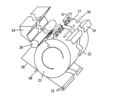
Reference is now made to Fig. 1, which is a simplified illustration of laser
writing apparatus constructed and operative in accordance with a preferred
embodiment
of the present invention. The laser writing apparatus typically comprises a
laser scanning
unit 20, illustrated in Fig. 2, which writes a latent image 21 onto a
photoreceptor 22,
which is typically located on the cylindrical surface of a drum 23.
The photoreceptor 22, bearing the latent image 2I, receives toner from a
toner hopper 24 via a developer roller 26 and transfers the toner onto a
substrate 28 with
the assistance of a transfer corotron 30. The toner is fused onto the
substrate by a fuser
32. A discharge lamp 34 serves to discharge the photoreceptor 22. Downstream
of
discharge lamp 34, a charge corotron 36 uniformly charges the photoreceptor,
upstream
of impingement thereon of laser beams 37 from laser scanning unit 20, which
selectively
discharges regions on the photoreceptor, thus creating the latent image 21.
It is a particular feature of the present invention that the laser scanning
unit 20, as illustrated in Fig. 2, comprises a selectably directable optical
beam deflector
including a base 50 onto which are mounted a plurality of substrates 52, each
having
formed thereon a multiplicity of waveguides 54, preferably 256 in number, each
waveguide 54 preferably receiving tight and emitting light having a selectable
phase,
intensity or a combination thereof. The totality of light emitted by the
multiplicity of
waveguides 54 on each substrate 52 is supplied to an output lens 55, which
produces a
selectably directable output beam 56, which covers a given sector of the
photoconductor.
The various substrates cooperate to cover the entire useful area of the
photoconductor.
It is a particular feature of the present invention that the substrates 52
need not be aligned on base 50 to a very high degree of accuracy, inasmuch as
the
orientations of beams 56 produced thereby are electronically deternuned and
adjustable,
inter olio to take misalignment into account.
At least one sequential multiplexer 58 applies electrical inputs to each
substrate 52 for individually controlling the light emitted by each of the
multiplicity of
CA 02294208 1999-12-22
WO 98/59276 PCT/IL98/00293
waveguides 54, thereby governing the orientation of said selectably directable
output
beam 56. Preferably, the sequential multiplexes 58 is a phase controller which
controls
the phase of the light emitted by each of the multiplicity of waveguides.
Alternatively
multiplexes 58 may be an intensity controller or a combination phase/intensity
controller.
Multiplexes 58 may be on a substrate separate from or integral with substrate
52.
An input light source 60, such as a diode laser or an optical fiber,
provides a light beam 62 which impinges on an input lens assembly 64, a
preferred
embodiment of which is illustrated in Fig. 7. The input lens assembly 64
provides a multi-
plicity of focused beams 65, each of which impinges on one of the waveguides
54 on
substrate 52.
As seen in Fig. 7, the input lens assembly 64 typically comprises a
combination of a cylindrical lens 66 and an array of cylindrical microlenses
67 bonded
thereto. The output lens 55 typically comprises mutually perpendicularly
aligned
cylindrical lenses 68 and 69.
Reference is now made to Figs. 3A and 3B, which illustrate two
alternative embodiments of an integrated optics scanning unit forming part of
the
scanning engine of Fig. 2. In the embodiment of Fig. 3A, an input laser 70,
such as a
diode laser, receives a laser control signal from content control electronics
(not shown)
and provides a laser beam 72 which impinges on an input lens assembly 74, a
preferred
embodiment of which is illustrated in Fig. 7.
The input lens assembly 74 provides a multiplicity of focused beams 76,
each of which impinges on one of the waveguides 54 on substrate 52. Each
waveguide
54 receives an electrical input via a corresponding conductor 78, which
extends from the
waveguide to a corresponding connector pad 80 which is also formed on
substrate 52. A
sequential multiplexes 58 (Fig. 2), formed on a separate substrate 82 receives
address
information via an address bus 84 and a phase, intensity, or phase/intensity
input via an
input line 86 from control electronics (not shown) and supplies a phase,
intensity, or
21
CA 02294208 1999-12-22
WO 98/59276 PCT/IL98/00293
phase/intensity control signal to each waveguide 54 via a conductor 88 and a
corresponding connector pad 80 and conductor 78.
The phase, intensity or phase/intensity controlled outputs 90 of each of
the waveguides 54 are combined in an output lens 92 and produce a focused
output
beam 94, whose direction is controlled by the phase, intensity or
phase/intensity inputs
supplied via multiplexes 58.
The embodiment of Fig. 3B is identical to that of Fig. 3A other than in
that multiplexes 58 (Fig. 2) is not embodied on a separate substrate from that
on which
the waveguides 54 are formed, as in Fig. 3A. In the embodiment of Fig. 3B,
waveguides
54 and sequential multiplexes 58 are both embodied on a single substrate 100
and thus
connector pads 80 may be eliminated. The remaining elements of Fig. 3B may be
identical to those in Fig. 3A and are indicated by the same reference
numerals.
According to an alternative embodiment of the present invention, input
and output lenses 74 and 92 may be eliminated. Other types of optical
couplers, known
in the art, may be employed instead.
Reference is now made to Fig. 4, which is a simplified illustration of
optical switching apparatus constructed and operative in accordance with a
preferred
embodiment of the present invention. The optical switching apparatus
preferably
comprises an optical interconnect unit 110 which is connected to a
multiplicity of ports
112, most or each of which has a data output line 114, an address output Line
116 and a
data input line 118, as well as a, preferably duplex, information conduit 120
which can be
of any suitable form, such as, for example, copper or fiber and which can
receive data in
any suitable format. Some of the ports 112 may lack a data input line or may
lack a data
output line and an address output line.
When optical fibers are employed as data output lines 114, it is preferred
that polarization maintaining fibers be employed in conjunction with polarized
lasers or
other polarized light sources. This eliminates polarization sensitivity of the
beam
deflection.
22
CA 02294208 1999-12-22
WO 98/59276 PCT/IL98/00293
Preferably clock synchronization is maintained between the input and
output portions of each of ports 112 and between the various ports 112.
The optical interconnect unit 110, a preferred embodiment of which is
illustrated in Fig. 5, comprises a beam deflector assembly array 122 and a
beam receiving
assembly array 124. Each beam deflector assembiy in array I22 receives data
and address
inputs from a port 112 and each beam receiving assembly in array 124 provides
a data
input to a port 112.
It is a particular feature of the present invention that the optical
interconnect unit 110, as illustrated in Fig. 5, comprises a selectably
directable optical
beam deflector including a base 150 onto which are mounted a plurality of
substrates
152, each having formed thereon a multiplicity of waveguides 154, preferably
256 in
number, each waveguide I54 preferably receiving light and emitting sight
having a
selectable phase. The totality of light emitted by the multiplicity of
waveguides 154 on
each substrate 152 produces a selectably directable output beam 156.
Also preferably mounted on base 150 is the beam receiving assembly
array 124. Each beam receiving assembly 158 preferably comprises a beam
receiving lens
160 which couples a received beam onto an output fiber 162, which is
preferably a
flexible fiber. Alternatively, the output fiber 162 may be replaced by a
suitable light
detector.
It is a particular feature of the present invention that the substrates 152
and the beam receiving assemblies 158 need not be aligned on base 150 to a
very high
degree of accuracy, inasmuch as the orientations of beams 156 produced thereby
is
electronically determined and adjustable, inter alia to take into misalignment
into
account.
At least one sequential multiplexer 168 applies electrical inputs to each
substrate 152 for individually controlling the light emitted by each of the
multiplicity of
waveguides 154, thereby governing the orientation of the selectably directable
output
beam 156.
23
CA 02294208 1999-12-22
WO 98/59276 PCT/IL98/00293
Preferably, the sequential multiplexer 168 is a phase controller which
controls the phase of the light emitted by each of the multiplicity of
waveguides.
Alternatively, multiplexer 168 is an intensity or phase/intensity controller.
Reference is now made to Figs. 6A and 6B, which illustrate two
alternative embodiments of an integrated optics switching unit forming part of
the cross-
connect assembly of Fig. 5. In the embodiment of Fig. 6A, an input optical
fiber 170
provides a beam 172 which impinges on an input lens assembly 174, a preferred
embodiment of which is illustrated in Fig. 7.
The input lens assembly 174 provides a multiplicity of focused beams 176,
each of which impinges on one of the waveguides 154 on substrate 152. Each
waveguide
154 receives an electrical input via a corresponding conductor 178, which
extends from
the waveguide to a corresponding connector pad 180 which is also formed on
substrate
152. A sequential multiplexer 168 (Fig. S), formed on a separate substrate
182, receives
address information via an address bus 184 and a phase, intensity or
phase/intensity input
via an input line 186 from control electronics (not shown) and supplies a
phase, intensity
or phase/intensity control signal to each waveguide 154 via a conductor 188
and a
corresponding connector pad 180 and conductor 178.
The phase, intensity or phase/intensity controlled outputs 190 of each of
the waveguides 154 are combined in an output lens 192 and produce a focused
output
beam 194, whose direction is controlled by the phase, intensity or
phase/intensity inputs
supplied via multiplexer 168.
The embodiment of Fig. 6B is identical to that of Fig. 6A other than in
that sequential multiplexer 168 (Fig. 5) is not embodied on a separate
substrate from that
on which the waveguides 154 are formed, as in Fig. 6A. In the embodiment of
Fig. 6B,
waveguides 154 and sequential multiplexer 168 are both embodied on a single
substrate
200 and thus connector pads 180 may be eliminated. The remaining elements of
Fig. 6B
may be identical to those in Fig. 6A and are indicated by the same reference
numerals.
24
CA 02294208 1999-12-22
WO 98/59276 PCT/IL98/00293
Reference is now made to Figs. 8A and 8B. Fig. 8A is a perspective
illustration of a waveguide unit useful as part of the integrated optics beam
deflection
unit of Fig. 7, while Fig. 8B is a detailed sectional illustration of a pair
of waveguides
forming part of the waveguide unit of Fig. 8A. It is seen from a consideration
of Figs. 8A
and 8B that substrate 52 (Figs. 2 & 7) is preferably formed of an N doped GaAs
layer
250 having formed on the bottom thereof an N-type ohmic contact 252, typically
com-
prising evaporated Ni/GeAu/Ni/Au. Formed over layer 250 is a cladding layer
254,
preferably formed of N doped AIGaAs.
The waveguide 54 is based on layer 254 and includes a core layer 256
comprising a GaAs PN junction defined by an N layer 258 and a P layer 260. A
cladding
layer 262, preferably formed of P doped AIGaAs, is preferably formed over
layer 260. A
cap layer 264, preferably formed of P+ doped GaAs, is preferably formed over
layer 262.
Along the length of the waveguides there are provided P-type ohmic
contacts 266, typically formed of Ti/Au. Adjacent waveguides 54 are separated
from
each other by etching. The resultant gaps are indicated by reference numeral
268.
A polyimide insulative layer 270 is preferably formed over layer 266, fills
gaps 268, and defines intermittent discrete apertures 272. Intermitted strips
of a metal
layer 274 are formed over the polyimide insulative layer 270 and contact the
ohmic
contacts 266 through discrete apertures 272 in the poiyimide layer 270. The
intermittent
strips provide individual mutually insulated electrical pathways communicating
with each
of the waveguides 54 separately. These pathways are designated by reference
numeral 78
in Figs. 3A and 3B and by reference numeral 178 in Figs. 6A and 6B.
It is appreciated that the depth of gaps 268 defined by etching may vary
such that layers 250, 254, 258 and 260 may or may not be etched to define gaps
and
waveguides. It is to be appreciated that waveguides 54 may also be provided by
any
other suitable technique, such as, for example, ion implantation.
CA 02294208 1999-12-22
WO 98/59276 PCT/IL98/00293
Waveguide structures of this general type are described in the following
publication, and the references cited therein, the disclosures of which are
hereby
incorporated by reference:
J. G. Mendoza-Alvarez et al, Analysis of Depletion Edge Translation
Lightwave Modulators, IEEE Journal of Lightwave Technology Vol. 6, No. 6, June
1988, pp. 793 - 808.
Reference is now made to Figs. 9A, 9B, 9C and 9D, which are graphs
illustrating a simulation of the far-field diffraction and interference
pattern produced by
an optical beam deflector constructed and operative in accordance with a
preferred
embodiment of the present invention for different applied voltages. The
simulation is for
an optical beam deflector which includes 256 waveguides having a pitch between
adjacent waveguides of 9 microns. The width of each waveguide is 3 microns and
the
wavelength of the light passing through the deflector is 1.3 microns.
Figures 9A, 9B, 9C and 9D illustrate the far-field diffraction and
interference patterns for phase shifts between adjacent waveguides of 0; ~/2;
n; and
3~/2, respectively.
It can be seen from a consideration of Figs. 9A - 9D that the relative
phase of each of the waveguides determines the angular location of given lobes
of the
interference pattern, while the diffraction pattern defines an intensity
envelope which
does not vary with phase but causes different angular locations to have
different
intensities.
It is a particular feature of the present invention that the ratio between the
angular width of each of the lobes and the angular separation between adjacent
lobes is
very substantial, due to the fact that the invention enables a very large
number of
waveguides ( typically 256) to be formed on a substrate and individually
operated.
This high ratio enables a correspondingly high level of resolution to be
realized in various applications, such as scanning and switching, providing a
high number
of individually addressable scanning and switching locations.
26
CA 02294208 1999-12-22
WO 98/59276 PCT/IL98/00293
It may also be appreciated by persons skilled in the art that the peak signal
to background ratio is very high due to large number of waveguides employed.
Reference is now made to Fig. 10 which is an illustration of an optical
multiplexer providing sequential voltage inputs to multiple waveguides forming
part of a
beam deflection unit in accordance with a preferred embodiment of the present
invention.
As seen in Fig. 10, each waveguide 54 intermittently receives an electrical
input via an electrical pathway, such as pathway 78 (Figs. 3A and 3B) or 178
(Figs. 6A
and 6B). The electrical input is preferably supplied from the drain 301 of a
FET
transistor 300 whose gate 302 is coupled to the output of an AND gate 304. The
source
of each FET transistor 300 receives a phase, intensity or phase/intensity
input from an
analog voltage line 306, identified by reference numeral 86 in Figs. 3A and 3B
and by
reference numeral 186 in Figs. 6A and 6B.
Each AND gate 304 receives a plurality of digital address inputs via NOT
gates 308 from an address bus 310, which is identified by reference numeral 84
in Figs.
3A and 3B and by reference numeral 184 in Figs. 6A and 6B. Each AND gate 304
is
differently configured such that every available combination of address inputs
causes a
different single AND gate to provide an electrical output to a corresponding
gate of a
corresponding FET transistor 300.
It is a particular feature of the present invention that the multiplexer
sequentially provides individual phase, intensity or phase/intensity inputs to
the individual
waveguides, using digital address coding, thus enabling a very large number of
waveguides to be individually addressed.
Reference is now made to Fig. 11, which illustrates the wavelength
dependency of the angular location of the diffraction orders. This wavelength
dependency may be employed advantageously in accordance with a preferred
embodiment of the present invention to provide wavelength division
multiplexing
(WDM). In this manner multiple information channels may be sent over a single
physical
fiber by transmitting each channel along a separate wavelength.
27
CA 02294208 1999-12-22
WO 98/59276 PCT/IL98/00293
Reference is now made to Fig. I2, which illustrates wavelength division
multiplexing apparatus constructed and operative in accordance with a
preferred
embodiment of the present invention.
The wavelength division multiplexing apparatus 410 preferably comprises
a beam diffractor assembly array 422 and a beam receiving assembly array 424.
Each
beam difFractor assembly in array 422 receives data and address inputs from a
port and
produces a light beam having multiple wavelength components and each beam
receiving
assembly in array 424 provides a data input to a port.
It is a particular feature of the present invention that the wavelength
division multiplexing unit 410, as illustrated in Fig. 12, comprises an
optical beam
diffractor, which preferably also operates as a selectably directable optical
beam deflector
and includes a base 450 onto which are mounted a plurality of substrates 452,
each
having formed thereon a multiplicity of waveguides 454, preferably 256 in
number, each
waveguide 454 preferably receiving light and emitting light in a plurality of
beams
according to their wavelength. The totality of light emitted by the
multiplicity of
waveguides 454 on each substrate 452 preferably produces a plurality of
selectably
directable output beams, here indicated as beams 456 and 457.
Also preferably mounted on base 450 is the beam receiving assembly
array 424. Each beam receiving assembly 458 preferably comprises a beam
receiving lens
460 which couples a received beam onto an output fiber 462, which is
preferably a
flexible fiber. Alternatively, the output fiber 462 may be replaced by a
suitable light
detector. Each beam receiving assembly preferably receives a beam of a
different
wavelength.
It is a particular feature of the present invention that the substrates 452
and the beam receiving assemblies 458 need not be aligned on base 450 to a
very high
degree of accuracy, inasmuch as the orientations of beams 456 produced thereby
is
electronically determined and adjustable, inter alia to take into misalignment
into
account.
28
CA 02294208 1999-12-22
WO 98/59276 PCT/IL98/00293
Reference is now made to Fig. 13, which is a simplified flowchart
illustrating the manufacture of a waveguide device of the type shown in Fig.
8B, in
accordance with a preferred embodiment of the present invention. As indicated
in Fig. 13
a mufti-layer gallium arsenide wafer, such as that illustrated in Fig. 8B and
including
layers 250, 254, 258, 260, 262 and 264, is coated with metal to provide a
layer such as
layer 252 (Fig. 8B}. This initial stage is illustrated in Fig. 14A, wherein
the wafer is
designated by reference numeral 500 and the metal layer is illustrated by
reference
numeral 502.
The waveguiding regions of the waver, e.g. layers 258, 260, 262 and 264
(Fig. 8B) are configured preferably by standard photolithography and reactive
ion
etching. This stage is illustrated in Fig. 14B, where the waveguiding regions
are indicated
by reference numeral 504.
It is a particular feature of the invention that the front side of the wafer,
i.e. the top surfaces 506 of waveguiding regions 504 and the top surfaces 508
of the
recesses 510 therebetween, is selectively coated with metal by evaporation in
a direction
generally perpendicular thereto, the direction being selected with respect to
interconnecting surfaces 512 which interconnect the upper and lower surfaces
506 and
508 respectively such that metal is not substantially coated onto the
interconnecting
surfaces 512, whereby electrical connections between the upper and lower
surfaces 506
and 508 via the interconnecting surfaces 512 are not formed by the metal
coating. The
metal layer, which is designated by reference numeral 266 in Fig. 8B, is
indicated by
reference numeral 514 in Fig. 14C.
Following formation of 514 by evaporation as aforesaid, one or more
conductive layers, separated from each other and from metal layer 514 by
insulative
layers, are preferably provided. A conductive layer is indicated in Fig. 8B by
reference
numeral 274 and in Fig. 14D by reference numeral 516 and an insulative layer
is
indicated in Fig. 8B by reference numeral 270 and in Fig. 14D by reference
number 518.
Vias 520 are preferably provided to interconnect conductive layers, such as
layer 516,
29
CA 02294208 1999-12-22
WO 98/59276 PCT/IL98/00293
with layer 514 through insulative layer 518. As seen in Fig. 14E, the outlines
of the
monolithic device may then be defined by cleaving and dicing.
Reference is now made to Fig. 15, which is a simplified illustration of a
polarization-independent waveguide constructed and operative in accordance
with a
preferred embodiment of the present invention. The waveguide of Fig. 15 is
characterized in that it is formed of at least two elongate portions 530 and
532, separated
by a gap 534. Gap 534 is preferably smaller than the wavelength of the light
guided by
the waveguide. A DC voltage V 1 of a first polarity is applied to elongate
portion 530,
while a DC voltage V2 of a second polarity, opposite to the first polarity, is
applied to
elongate portion 532. Gap 534 need not be a cut or other physical separation,
but may be
only an electrical or conductive separation.
It is known that the presence of an electric field in a gallium arsenide
waveguide changes the phase of light passing through the waveguide. The
resulting
change in phase differs with the polarization of the light, whereby for a
given electric
field light of one polarization, such as light in a TE mode is phase shifted
more than light
of polarization perpendicular thereto, such as light in a TM mode.
It has been appreciated by the present inventors that by switching the
direction of the electric field, the effect thereof on Iight in the TE and TM
modes is
reversed. This can be seen from a consideration of Figs. 16A and 16B, which
illustrate
the phase shifts produced in mutually perpendicularly polarized light by
electric fields of
opposite polarity.
Thus, if an electric field in a first direction causes a greater phase change
for light in a TE mode than for light in a TM mode, an electric field in a
second direction,
opposite to the first direction, causes a greater phase change for light in a
TM mode than
for light in a TE mode.
Accordingly, by first applying an electric field in a first direction to light
guided along the waveguide and then applying an electric field in a second
direction,
CA 02294208 1999-12-22
WO 98/59276 PCT/IL98/00293
opposite to the first direction, to that light, the effect of polarization on
the phase change
of the light is neutralized. This is visualized in Fig. 16C.
It is appreciated that the two electrical fields need not necessarily be
opposite in order to neutralize the effect of polarization as aforesaid. The
desired
neutralization may be realized empirically even with electric fields which are
not
opposite.
Reference is now made to Fig. 17, which is a simplified illustration of a
polarization-independent waveguide constructed and operative in accordance
with
another preferred embodiment of the present invention. The waveguide of Fig.
17 is
characterized in that it is formed of two elongate portions 550 and 552 of
identical
length, separated by a quarter wave plate 554. The quarter wave plate is
operative to
rotate the polarization direction of light guided along the waveguide by 90
degrees,
therefore shifting the TM component to a TE component and vice versa.
Thus light traveling along the entire waveguide has the same phase
change irrespective of its polarization upon entry to the waveguide.
Reference is now made to Fig. 18, which is a simplified illustration of a
polarization-independent waveguide constructed and operative in accordance
with yet
another preferred embodiment of the present invention. In this embodiment,
there is
provided a selectably directable optical beam deflecting device comprising a
substrate
570 having formed thereon a multiplicity of electrically controlled, phase-
shifting
waveguides 572, such as waveguides of the type described hereinabove with
reference to
Figs. 8A and 8B.
In accordance with a preferred embodiment of the present invention there
is also formed on substrate 570 a light receiver 574 for directing light into
the
multiplicity of waveguides 572. Preferably, the light receiver comprises a
selectable
polarization rotator 576. In accordance with a preferred embodiment of the
present
invention, the selectable polarization rotator is automatically operative to
rotate the
31
CA 02294208 1999-12-22
WO 98/59276 PCT/IL98/00293
polarization so as to provide an optimized light output from the multiplicity
of
waveguides.
Preferably, the selectable polarization rotator is responsive to an output of
the multiplicity of waveguides. Alternatively, the selectable polarization
rotator is
responsive to the polarization of an input to the multiplicity of waveguides.
The selectable polarization rotator is preferably embodied in a gallium
arsenide voltage controlled waveguide, which may be constructed in a manner
similar or
identical to that described hereinabove.
Reference is now made to Fig. 19, which is a simplified illustration of a
polarization-independent waveguide constructed and operative in accordance
with still
another preferred embodiment of the present invention. This embodiment is
characterized in that a polarization rotator 590 rotates the polarization of
light passing
through a multiplicity of electrically controlled, phase-shifting waveguides
592 by 90
degrees. Preferably, the polarization rotator 590 comprises a magnetic field
source pro-
ducing a magnetic field B, whose axis lies parallel to the longitudinal axes
of the
waveguides 592. The magnetic field B is typically produced by the flow of an
electric
current i, as shown in Fig. 19.
In this way, light guided along the waveguide has its polarization shifted
by 90 degrees, therefore shifting the TM component to a TE component and vice
versa.
Thus light traveling along the entire waveguide has the same phase
change irrespective of its polarization upon entry to the waveguide.
As in the embodiment of Fig. 18, in accordance with a preferred
embodiment of the present invention, the selectable polarization rotator 590
is
automatically operative to rotate the polarization so as to provide an
optimized light
output from the multiplicity of waveguides 592.
Preferably, the selectable polarization rotator 590 is responsive to an
output of the multiplicity of waveguides 592. Alternatively, the selectable
polarization
32
CA 02294208 1999-12-22
WO 98/59276 PCT/IL98/00293
rotator 590 is responsive to the polarization of an input to the multiplicity
of waveguides
592.
Reference is now made to Fig. 20, which is a simplified illustration of an
optimal waveguide structure for a given wavelength in accordance with a
preferred
embodiment of the present invention. Fig. 20 illustrates an optimal
distribution of Gght in
the waveguide of Fig. 8B. The light intensity is illustrated by trace 598.
Preferably, the
waveguide is constructed such that most of the light is confined in layers 256
(Fig. 8B).
Little or no light is to be allowed in conductive layers 266 and 252.
Techniques for
confining light in layers 256 are well known in the art and need not be
described herein.
It is additionally preferred that a P-N junction 600 be defined in layers
256 as indicated in Fig. 8B.
Reference is now made to Fig. 21, which is a simplified illustration of part
of a waveguide device having multiple conductors constructed and operative in
accordance with a preferred embodiment of the present invention. In the
embodiment of
Fig. 21, there is provided a substrate 610 having formed thereon a
multiplicity of phase-
shifting waveguides 612. A light receiver (not shown) directs light into the
multiplicity of
waveguides. The substrate 610 comprises multiple mutually insulated conductor
layers
614, which are insulated by insulative layers 616 and are connected to said
waveguides
by vias 618. Vias 618 are constructed layer by layer and are interconnected
via pads 620.
Reference is now made to Fig. 22, which is a simplified illustration of part
of a monolithic laser and waveguide structure constructed and operative in
accordance
with a preferred embodiment of the present invention. Such monolithic
structure are
believed to be novel. The structure of Fig. 22 preferably comprises a
substrate 620
having formed thereon a multiplicity of waveguides 622, of which only one is
shown, and
a laser 624, monolithically formed on the substrate 620 and providing light to
the
multiplicity of waveguides 622.
The laser 624 preferably is constructed in accordance with the foregoing
description of Fig. 8B and includes:
33
CA 02294208 1999-12-22
WO 98159276 PCT/IL98/00293
an N-doped gallium arsenide substrate 626;
an N-doped aluminum gallium arsenide layer 628 formed over substrate
626;
an N-doped gallium arsenide layer 630 formed over the N-doped
aluminum gallium arsenide layer 628;
a P-doped gallium arsenide layer 632 formed over the N-doped gallium
arsenide layer 630;
a P-doped aluminum gallium arsenide layer 634 formed over the P-doped
gallium arsenide layer 632; and
a P-doped gallium arsenide layer 636 formed over the P-doped aluminum
gallium arsenide layer 634.
It is a particular feature of the present invention that the fact that the
waveguide structure of Fig. 8B can be operated as a light source, enables
greatly
enhanced ease of alignment of the waveguide with respect to external optics,
since the
waveguide can produce a beam of light during alignment thereof.
Reference is now made to Fig. 23, which is a simplified illustration of part
of a waveguide device having tapered inputs. The structure of Fig. 23 can be
used as part
of a selectably directable optical beam deflecting device and includes a
substrate 650
having formed thereon a multiplicity of waveguides 652 and a light receiver
654 directing
light into the multiplicity of waveguides at first ends thereof. The structure
is
characterized particularly in that the multiplicity of waveguides 652 are
outwardly
tapered at said first ends thereof 656 at which light enters the waveguides.
Preferably,
the light receiver employs a cylindrical lens 658. It is appreciated that the
structure of
Fig. 23 may be used as a light output structure and not only as a light input
structure.
Reference is now made to Fig. 24, which is a simplified illustration of a
waveguide device having a mufti-mode interference coupler including a tapered
input
waveguide. The structure of Fig. 24 is an alternative to the structure of Fig.
23 and
includes a substrate 670 having formed thereon a multiplicity of waveguides
672. Here a
34
CA 02294208 1999-12-22
WO 98/59276 PCT/IL98/00293
light receiver 674 comprising a mufti-mode interference coupler 676 directs
light into the
multiplicity of waveguides 672.
Preferably, the mufti-mode interference coupler comprises a light
receiving waveguide 678 which includes a light receiving end 680 which may be
outwardly tapered. Light which is received at light receiving end 680 is
typically coupled
from an optical fiber 682. The optical fiber 682 has preferably a matching
output end 683
for coupling to the receiving end 680.
Reference is now made to Fig. 25, which is a simplified illustration of
wave propagation in a waveguide device of the type shown in Fig. 24, having a
multi-
mode interference coupler. It is seen that in the mufti-mode interference
coupler,
designated by reference numeral 690, the waves interfere both constructive and
destructively. By suitably selecting the dimensions of the mufti-mode
interference coupler
690, as well known in the art, it can be ensured that constructive
interference takes place
at a number of locations 692 at the interface 694 between the mufti-mode
interference
coupler and the waveguide.
In accordance with a preferred embodiment of the present invention the
waveguides 696 are constructed such that their entrances 698 are aligned with
locations
692, thereby maximizing the coupling e~ciency between the mufti-mode
interference
coupler 690 and the waveguides 696.
In accordance with a preferred embodiment of the present invention, the
input waveguide 700 to the mufti-mode interference coupler 690 may be
operative as an
electro-absorption modulator, the fiznctionaIity of which is well-known in the
art.
Reference is now made to Fig. 26, which is a simplified illustration of
wave propagation in a waveguide device having a free-space input coupler 710.
The
waveguide device may be identical to that of Figs. 24 and 25 in structure and
function
other than in that the dimensions of the free-space input coupler 710 are not
such that
interference occurs therewithin. Rather the light propagates freely
therethrough as shown
to the interface 712 with waveguides 714. In accordance with a preferred
embodiment of
3~
CA 02294208 1999-12-22
WO 98/59276 PCT/IL98/00293
the present invention, the entrance 716 of each waveguide 714 is outwardly
tapered, so
as to enhance coupling efFlciency.
As seen in Fig. 27, the waveguide devices described hereinabove with
reference to Figs. 23, 24, 25 and 26 may be employed in optical switches both
as
selectably directable optical beam deflection devices 730 at the input end 734
and as
selectably directable receiving devices 736 at the output end 738.
Reference is now made to Fig. 28, which is a simplified illustration of a
monolithic device having both electronic and optical functionality. The
embodiment of
Fig. 28 provides an active optical beam transnussion device comprising at
least one
substrate 750 having formed thereon a multiple layer integrated electronic
circuit 752
and a multiplicity of electrically controlled waveguides 754.
In accordance with a preferred embodiment of the present invention, the
waveguides 754 emit a selectably directable beam of light or selectabiy
receive a beam of
light.
Reference is now made to Fig. 29, which is a simplified illustration of part
of an optical switch including a monolithic plurality of selectably directable
optical beam
deflecting devices 760 in accordance with one preferred embodiment of the
present
invention. It is thus appreciated that in the embodiment of Fig. 29 all of the
devices 760
are formed on a single substrate 762. Each of devices 760 may be substantially
identical
to the devices described hereinabove with reference to either of Figs. 23 and
24.
In the embodiment of Fig. 29, the electronic connection pads 764 are
located adjacent each individual device 760.
Fig. 30 is a simplified illustration of part of an optical switch including a
monolithic plurality of selectably directable optical beam deflecting devices
in accordance
with another preferred embodiment of the present invention. It is similar to
the
embodiment of Fig. 29 other than in that the electronic connection pads 774
for aII of the
selectably directable optical beam deflecting devices 776 are all located
adjacent the
edges 778 of the common substrate 780.
36
CA 02294208 1999-12-22
WO 98/59276 PCT/IL98/00293
Reference is now made to Fig. 31, which is a simplified illustration of part
of an optical switch including a monolithic plurality of selectably directable
optical beam
deflecting devices in accordance with yet another preferred embodiment of the
present
invention. Here, the electrical connection pads 794 are formed over part of
the selectably
directable optical beam deflecting waveguide devices 796.
Reference is now made to Fig. 32, which is a simplified illustration of a
waveguide device having a light coupler 800, of the type described hereinabove
with
reference to any of Figs. 24 - 26 including an input waveguide 802 functioning
as an
electro-absorption modulator. The embodiment of Fig. 32 also includes a light
detector
804 providing a modulating output 806 to the electro-absorption modulator
waveguide
802. Preferably, the light detector 804 receives a light input from an
information carrying
modulated light source 808.
The electro-absorption modulator waveguide 802 of Fig. 32 may serve as
an electro-absorption modulator in the embodiments of Figs. 24 - 26. The light
detector
804 is preferably monolithically formed together with the eIectro-absorption
modulator
waveguide 802 on the same substrate.
Reference is now made to Fig. 33, which is a simplified illustration of a
beam deflector including a waveguide structure in accordance with a preferred
embodiment of the present invention. The beam deflector of Fig. 33 is
characterized in
that it includes a spherical output lens 820 which receives light from a
cylindrical lens
822. Cylindrical lens 822 is optically coupled to a multiplicity of waveguides
824 and is
operative to direct the light received from waveguides 824 in a direction
perpendicular to
the plane of waveguides 824. The spherical output lens 820 focuses the light
received
from the cylindrical lens 822.
Similarly to the structure described above with reference to Fig. 23, the
waveguides 824 receive light from a cylindrical lens 826 which, in turn,
receives light
from the end 828 of an optical fiber 830. Alternatively, the input structure
of the
waveguides 824 may be similar to that described above with reference to Fig.
24.
37
CA 02294208 1999-12-22
WO 98159276 PCT/IL98/00293
Reference is now made to Fig. 34, which is an illustration of operational
parameters of a waveguide device having lens functionality in accordance with
a
preferred embodiment of the present invention. Fig. 34 indicates that by
suitable selection
of the electrical inputs to the waveguide device of Fig. 33, the focusing
functionality of
the spherical lens 820 can be provided by the waveguides 824 and the spherical
lens 820
can be obviated.
Thus, it is appreciated that there is thus provided an optical waveguide-
lens including a substrate having formed thereon a multiplicity of
electrically controlled,
phase-shifting waveguides and an electrical control signal source providing
electrical
signals to the multipiicity of waveguides to cause them to have a desired lens
functionality.
Fig. 34 shows the phase shift produced by the electrical control signal as a
function of the waveguide number. It is seen that a lens functionality, a tilt
functionality
and a combined tens and tilt functionality may be realized by suitable
selection of
electrical control signals. It is appreciated that the lens functionality,
taken alone, or in
combination with the tilt functionality may be employed in any and all of the
embodiments of the invention described herein.
The present invention also provides an optical switch comprising a
plurality of selectably directable optical beam deflecting devices and a
plurality of optical
beam receiving devices.
Reference is now made to Fig. 35, which is a simplified illustration of part
of an optical cross-connect assembly constructed and operative in accordance
with a
preferred embodiment of the present invention. The embodiment of Fig. 35 is
particularly
characterized in that it includes a plurality of selectably directable optical
beam deflecting
devices 850, each comprising at least one substrate having formed thereon a
multiplicity
of waveguides. Optical beam deflecting devices of this type are described
hereinabove
with reference to Fig. 23 and 24.
38
CA 02294208 1999-12-22
WO 98/59276 PCT/IL98/00293
The embodiment of Fig. 35 is also particularly characterized in that it
includes a plurality of optical beam receivers 852. Optical beam receivers 852
may be
optical fiber ends, as seen in Fig. 35. The optical fibers may be single mode
or multi-
mode fibers and their ends may have small numerical apertures. Alternatively,
optical
beam receivers 852 may be light detectors or selectably directable light
receivers, as
described hereinabove with reference to Fig. 27.
In the embodiment of Fig. 35, at an input side 854, a plurality of
selectably directable optical beam deflecting devices 850 is arranged, each to
receive
light from a suitably positioned optical fiber end 856. It is noted that
devices 850 are
mounted on a substrate 858, such as a mufti-layer ceramic substrate, onto
which are also
mounted control electronics 860.
Light coupling between optical fiber ends 856 and beam deflection
devices 850 may be achieved using a microlens array 862, as shown. The
microlens array
862 may comprise a combination of cylindrical lenses arranged in two
perpendicular
directions. The microlens array 862 provides focusing in two mutually
perpendicular
directions with different optical power. Where devices 850 are similar to
those described
in Fig. 23, the microlens array 862 provides output beams which are collimated
in a
direction parallel to the plane of the devices 850. Where devices 850 are
similar to those
described in Fig. 24, the microlens array 862 provides output beams which are
focused in
a direction parallel to the plane of the devices 850.
Although a single row of cylindrical lenses is shown in Fig. 3 5, it is
appreciated that a double row of cylindrical lenses may alternatively be
employed.
Alternatively, the microlens array 862 may be obviated and individual
lenses may be formed or mounted onto the optical fiber ends 856.
Downstream of the plurality of selectably directable optical beam
deflecting devices 850 there is provided one or more cylindrical lenses 864
which have
essentially the same functionality as that provided by cylindrical lens 822 in
the embodi-
ment of Fig. 33. A spherical lens 866 receives light from the one or more
cylindrical
39
CA 02294208 1999-12-22
WO 98/59276 PCT/1L98100293
lenses 864 and has the functionality of spherical lens 820 in the embodiment
of Fig. 33.
Similarly to spherical lens 820, it may be obviated in a case where the
plurality of
selectably directable optical beam deflecting devices 850 are provided with a
lens
functionality.
It is appreciated that the input side 854 may function as an output side
rather than an input side. In such a case, the structures, such as optical
fiber ends,
functioning as light receivers 852 may function instead as light transmitters.
The light
transmitters may be static or directable.
Reference is now made to Fig. 36, which is a simplified illustration of an
optical cross-connect assembly constructed and operative in accordance with
another
preferred embodiment of the present invention. The optical cross-connect
assembly of
Fig. 36 is particularly characterized in that it includes a plurality of
monolithic pluralities
870 of selectably directable optical beam deflecting devices 872, as well as a
plurality of
optical beam receiving devices 874. The selectably directable optical beam
deflecting
devices 872 may be any of the devices described herein with reference to Figs.
23 - 34.
The monolithic pluralities 870 may be any of the structures described
hereinabove with
reference to Fig. 3 5.
In accordance with a preferred embodiment of the present invention, the
plurality of monolithic pluralities 870 of beam deflecting devices 872 are
arranged
generally parallel to one another along an axis 876 perpendicular to a plane
in which
selectable deflection of a light beam is produced thereby, which is the plane
of each of
the plurality of monolithic pluralities 870.
A focusing lens 878 receives light from the plurality of monolithic
pluralities 870 of beam deflecting devices 872 and focuses it onto the light
receiving
devices 874. The lens 878 may be one or more lenses and may have the
functionality of
lens 820 in the embodiment of Fig. 33. As such, it may be obviated by
inclusion of lens
functionality in the plurality of monolithic pluralities 870 of beam
deflecting devices 872.
CA 02294208 1999-12-22
WO 98/59276 PCT/IL98/00293
It is appreciated that the plurality of monolithic pluralities 870 'of beam
deflecting devices 872 and lens 878 may alternatively function as light
receivers rather
than a light transmitter. In such a case, the structures, such as optical
fiber ends,
functioning as light receivers 874 may function instead as light transmitters.
The light
transmitters may be static or directable.
Reference is now made to Fig. 37, which is a simplified illustration of an
optical cross-connect assembly constructed and operative in accordance with
yet another
preferred embodiment of the present invention. The optical cross-connect
assembly of
Fig. 37 is particularly characterized in that it includes a plurality of
monolithic pluralities
880 of selectably directable optical beam deflecting devices 882, as well as a
plurality of
optical beam receiving devices 884. The selectably directable optical beam
deflecting
devices 882 may be any of the devices described herein with reference to Figs.
23 - 34.
The monolithic pluralities 880 may be any of the structures described
hereinabove with
reference to Fig. 3 5.
Here the plurality of monolithic pluralities 880 of beam deflecting devices
882 are arranged generally distributed along a curve 886 extending in a plane
perpendicular to a plane in which selectable deflection of a Iight beam is
produced there-
by, which is the plane of each of the plurality of monolithic pluralities 880.
A focusing lens 888 receives light from the plurality of monolithic
pluralities 880 of beam deflecting devices 882 and focuses it onto the light
receiving
devices 884. The lens 888 may be one or more lenses and may have the
functionality of
lens 820 in the embodiment of Fig. 33. As such, it may be obviated by
inclusion of lens
functionality in the plurality of monolithic pluralities 880 of beam
deflecting devices 882.
It is appreciated that the plurality of monolithic pluralities 880 of beam
deflecting devices 882 and lens 888 may alternatively function as light
receivers rather
than a light transmitter. In such a case, the structures, such as optical
fiber ends,
functioning as light receivers 884 may function instead as light transmitters.
The light
transmitters may be static or directable.
41
CA 02294208 1999-12-22
WO 98/59276 PCT/IL98100293
Reference is now made to Fig. 38, which is a simplified illustration of an
optical cross-connect assembly of the type shown in any of Figs. 35 - 37 with
feedback
functionality. The embodiment of Fig. 38 comprises an optical switch input end
900
which receives modulated light from a multiplicity of fibers 902 and
selectably transmits
the modulated light to a multiplicity of light receivers 904, such as optical
fiber ends. The
switch input end 900 may be any suitable switch input end of the type
described herein
with reference to any ofFigs. 35, 36 & 37.
Signal pickup devices 906 receive at least one parameter of the signals
received by light receivers 904 and provide feedback input signals to a
feedback
processor 908. Output signals from the feedback processor 908 are operative to
govern
at least one parameter of the operation of the optical switch input end 900.
This feedback arrangement provides reduced crosstalk and enhanced
transmission efficiency.
The feedback input signals to feedback processor 908 may represent
received signal intensity and crosstalk. The parameters of operation of the
optical switch
input end 900 which are affected by output signals from the feedback processor
include
the phase shift produced by individual waveguides, the amount of rotation
produced by
the polarization rotator, such as rotator 576 (Fig. 18) or rotator 590 (Fig.
19). The
feedback processor 908 effectively provides a feedback connection between the
optical
beam receiving devices and the optical beam deflecting devices.
It is appreciated that the feedback functionality need not necessarily be
automatic but rather may involve some operator intervention.
Reference is now made to Fig. 39, which is a simplified illustration of an
optical cross-connect assembly constructed and operative in accordance with a
preferred
embodiment of the present invention. Here optical beam receiving devices 910
are
configured to receive light over a region 912 sufficiently large such that
wavelength
dependencies of optical beam deflectors 914 do not substantially affect the
amount of
light sensed by the receiving devices.
42
CA 02294208 1999-12-22
WO 98/59276 PCT/IL98/00293
Reference is now made to Fig. 40, which is a simplified illustration of an
optical cross-connect assembly constructed and operative in accordance with a
preferred
embodiment of the present invention. Here a multiplicity of waveguides 920 are
each
operative simultaneously to deflect a plurality of optical beams 922 and to
direct them to
a plurality of different receivers 924.
Reference is now made to Fig. 41, which is a simplified illustration of a
waveguide filter constructed and operative in accordance with a preferred
embodiment
of the present invention. The waveguide filter of Fig. 41 comprises a necked
waveguide
930 having a relatively broad input end 932 which receives light and allows
propagation
of mufti-mode light waves therethrough. When the mufti-mode light waves
encounter a
narrowed neck portion 934, the higher modes radiate outside the waveguide and
only the
modes which can propagate through the neck portion 934 pass therethrough to a
relatively broad output end 936. This filter can be used to efficiently remove
higher
modes which can cause crosstaik.
It is appreciated that the structures of Figs. 39, 40 and 41 may be applied
to any of the optical beam deflectors, optical beam receivers, cross-connect
assemblies
and optical switches described herein.
Reference is now made to Fig. 42, which is a simplified illustration of a
monolithic optical cross-connect assembly constructed and operative in
accordance with
a preferred embodiment of the present invention. A plurality of selectably
directable
optical beam deflecting devices 950 and a plurality of optical beam receiving
devices 952
are all monolithically formed on the same substrate 954.
It will be appreciated by persons skilled in the art that the present
invention is not limited to what has been particularly shown and described
hereinabove.
Rather the scope of the present invention includes both combinations and
subcombina-
tions of various features described hereinabove and shown in the drawings as
well as
modifications thereto and variations thereof which would occur to a person
skilled in the
art upon reading the description and which are not in the prior art.
43