Note: Descriptions are shown in the official language in which they were submitted.
CA 02294279 1999-12-22
WO 98/59528 PCT/US98/12694
EMISSIVE DISPLAY USING ORGANIC LIGHT EMITTING DIODES
Cross Reference to Related Patent Ap~iication
This application relates to and claims priority to U.S. Provisional
Application Serial No.
60/00,459. entitled "EMISSIVE DISPLAY USING ORGANIC LIGHT EMITTING DIODES"
filed on 3une 23, 1997.
Field of the Invention
The present invention relates to an Organic Light Emitting Device ("OLED")
video
display structure for a color video display or high brightness monochrome
display. More
specifically, the present invention relates to an OLED with a microcavity
structure for enhancing
light emission.
Background of the Invention
Organic light emitting devices have been known for approximately two decades.
OLEDs
work on certain general principles. An OLED is typically a laminate formed on
a substrate such as
soda-Iitne glass or silicon. A light-emitting layer of a luminescent organic
solid, as well as adjacent
I S semiconductor layers, are sandwiched between a cathode and an anode. The
semiconductor layers
may be hole-injecting or electron-injecting layers. The light-emitting layer
may be selected from
any of a multitude of fluorescent organic solids. The light-emitting layer may
consist of multiple
sublayers or a single blended layer.
When a potential difference is applied across the device. negatively charged
electrons move
from the cathode to the electron-injecting layer and finally into the layers)
of organic material. At
the same time positive charges, typically referred to as holes, move from the
anode to the hole-
injecting layer and finally into the same organic light-emitting layer(s).
When the positive and
negative charges meet in the layers) of organic material, they combine, and
produce photons.
The wave length -- and consequently the color -- of the photons depends on the
material
properties of the organic material in which the photons are generated. The
color of light emitted
from the OLED can be controlled by the selection of the organic material, or
by the selection of
dopants, or by other techniques known in the art. Different colored light may
be generated by
mixing the emitted light from different OLEDs. For example, white light is
produced by mixing
blue. red, and green light simultaneously.
1 -
- SUBSTITUTE SHEET (RULE 26)
CA 02294279 1999-12-22
WO 98159528 PCT/US98/12694
In a typical OLED, either the anode or the cathode is transparent in order to
allow the emitted
light to pass through to the viewer. The cathode is typically constructed of a
low work function
material. The holes are typically injected from the anode. a high work
function material, into the
organic material via a hole transport layer.
Typically, OLEDs operate with a DC bias of 2 to 30 volts. The OLED brightness
may be
controlled by adjusting the voltage or current supplied to the anode and
cathode. The relative
amount of light generated is commonly referred to as the "gray level." OLEDs
typically work best
when operated in a current mode. The light output is more stable for constant
current drive than for
a constant voltage drive. This is in contrast to many other display
technologies. which are normally
operated in a voltage mode. As a result. an active matrix display using OLED
technology, requires
a specific pixel architecture to provide for a current mode of operation.
In a typical matrix-addressed OLED device, numerous OLEDs are formed on a
sinele
substrate and arranged in groups in a regular grid pattern. Several OLED
groups forming a column
of the grid may share a common cathode, or cathode line. Several OLED groups
forming a row of
the grid may share a common anode, or anode line. The individual OLEDs in a
given group emit
light when their cathode line and anode line are activated at the same time. A
group of OLEDs
within the matrix may form one pixel in a display, with each OLED usually
serving as one subpixel
or pixel cell.
OLEDs have a number of beneficial characteristics. These include: a low
activation voltage
?0 {about ~ volts); fast response when formed with a thin light-emitting
layer; high brightness in
proportion to the injected electric current: high visibilit~.~ due to self
emission: superior impact
resistance; and ease of handling of the solid state devices in which they are
used. OLEDs, have
practical application in television, graphic display systems, and digital
printing. A I t h o a g h
substantial progress has been made in the development of OLEDs to date,
additional challenses
remain. For example, OLEDs continue to face a general series of problems
associated with their
long-term stability. In particular, during operation the layers of organic
film may undergo
recrystalizationor other structural changes that adversely affect the emissive
properties ofthe device.
Exposure to air and moisture presents unique problems with respect to OLEDs.
Exposing
a conventional OLED to the atmosphere shortens its life. The organic material
in the light-emitting
layers) reacts with water vapor. oxygen. etc. Lifetimes of x.000 to 35.000
hours have been obtained
for evaporated films and greater than x,000 hours for polymers. However, these
values are typically
2
SUBSTITUTE SHEET (RULE 26)
CA 02294279 1999-12-22
WO 98159528 PCT/CJS98/12694
reported for room temperature operation in the absence of water vapor and
oxygen. Lifetimes
associated with operations outside these conditions are typically much
shorter.
The low work function cathode is susceptible to oxidation by either water
vapor or oxygen.
Electroluminescence from oxidized areas is typically lower than other areas.
The anode may also
be affected by oxidation. The penetration of oxygen and moisture into the
interior of the OLED may
result in the formation of metal oxide impurities at the metal-organic
material interface. These metal
oxide impurities may cause separation of the cathode or anode from the organic
material. Dark, non-
emitting spots may appear at the areas of separation due to a lack of current
flow. Cathode materials
such as Mg-Ag or Al-Li are especially susceptible to oxidation.
To obtain a practical, useable OLED, it is necessary to protect the device, so
that water,
oxygen. etc., do not infiltrate the light-emitting layer or oxidize the
electrodes. Methods commonly
employed for protecting or sealing inorganic electroluminescent devices are
typically not effective
for sealing OLEDs. For example, in the "silicon oil method" of sealing
inorganic electroluminescent
devices, the silicon oil can infiltrate the light-emitting layer of an OLED,
the electrodes, and any
hole-injecting or electron-injecting layers. This may alter the organic light-
emitting layer, reducing
or eliminating its light emission properties. Likewise, resin coatings that
have been used to protect
inorganic EL devices are not suited for OLEDs. The solvent used in the resin
coating solution tends'
to i~ltrate the light-emitting layer of the OLED, degrading the light emission
properties of the
device.
Protective films may be used to seal OLEDs. For example, an electrically
insulating polymer
may be deposited on an outer surface of the OLED. Evaporated metal films are
also used to seal
OLEDs in a similar manner. Evaporated metal and polymer films are both
susceptible to pinholes.
To avoid pinholes these films must be relatively thick and hence result in
poor light transmission.
Accordingly, there remains a need for a method of sealing an OLED which does
not degrade light
emissions from the device.
Edge shorting between the cathode and anode layers is another problem
affecting most
conventional OLED devices. Edge shorting reduces the illumination potential of
the display. Edge
shorting is the channeling of light within the organic layers. As a result of
the channeling, light is
not directed toward the viewer. Also, when light is emitted at all forward
angles, i.e., in a
Lambertian manner, it may activate neighboring OLEDs reducing contrast or
color purity. Thus,
there is a need to develop a microcavity structure capable of limiting edge
shorting and increasing
illumination.
3
SUBSTITUTE SKEET (RULE 26)
CA 02294279 1999-12-22
WO 98/59528 PCT/US98/12694
A passive OLED matrix pulses light at high pixel brightness in order to
achieve moderate
overall brightness. An active OLED matrix with sustained application of
voltage across the anode
and cathode may produce the same brightness with a much lower pixel luminance.
However, in
order to achieve the same appearance as the passive matrix. the active matrix
must be refreshed
~ continuously. As a result, there is a need to provide a method of refreshing
an OLED display during
the time that the organic layers are exposed to the electrical potential
between, the anode and the
cathode.
A typical matrix of OLEDs experiences certain problems. As described above,
the OLEDs
located within the matrix may experience channelling. The channeling of light
in one OLED or
subpixel may cause the inadvertent activation of neighboring subpixels.
Furthermore, the proximity
of the subpixels within the matrix can cause a reduction in ambient light
contrast across the matrix.
The need exists for a matrix design with improved color purity and ambient
light contrast.
The present invention meets the needs set forth above, and provides other
benefits as well.
Objects of the Invention
Therefore it is an object of the present invention to provide an active matrix
design that
maximizes the peak luminance of an organic light emitting device.
It is another object of the present invention to reduce edge shorting in an
organic light
emitting device.
A further object of the present invention is to provide an organic light
emitting device
with improved luminance.
It is another object of the present invention to provide an organic light
emitting device with
improved light directionality.
A further object of the present invention is to provide a method and structure
for sealing
organic light emitting devices which provides a substantially moisture free
OLED without degrading
?5 light emissions.
It is a further object of the present invention to provide an organic light
emitting device with
relatively no reduction in illumination during periods of sustained activity.
Another object of the present invention is to provide a matrix of organic
light emitting
devices with improved color purity.
It is a further object of the present invention to provide a matrix of organic
light emitting
devices with high ambient light contrast.
4
CA 02294279 1999-12-22
WO 98/59528 PCT/US98/12694
Additional objects and advantages of the invention are set forth. in part. in
the description
which follows and, in part, will be apparent to one of ordinary skill in the
art from the description
and/or from the practice of the invention.
Summary of the Invention
In response to this challenge. Applicant has developed an innovative.
economical organic
light emitting device comprising: a substrate: a first conductor overlying the
substrate: a layer of
light emitting organic material overlying the first conductor: a second
conductor overlying the layer
of light emitting material; and a means for restricting light emission in
directions parallel to the
substrate. The device's substrate is substantially planar and may comprise a
silicon wafer. The
I O device may further comprise a means for connecting the silicon wafer to
the first conductor. The
means for restricting light emission may overlie the layer of light-emitting
organic material. The
means for restricting light emission may comprise either a layer of dielectric
material or a plurality
of layers of dielectric material. The means for restricting light emission may
also comprise either
a layer of transparent conductor material or multiple layers of transparent
conductor material which
15 overlie the first conductor and underlie the light emitting organic
material. The first conductor may
be planarized. Each of the plurality of layers of dielectric material may have
a different index of
refraction from that of any adjacent layer. The layers of dielectric may be
deposited or evaporated
at an angle to the substrate surface. Alternatively, the dielectric layers may
be constructed while the
substrate is rotating. The device may further comprise a transition layer
underlying the first
?0 conductor and a barner layer overlying the second conductor.
The barrier layer comprises a diamond-like carbon material and may function as
an electron
injector. The device of the present invention may further comprise a Better
layer overlying the
second conductor and underlying the barrier layer, and a sealing layer
overlying the barrier layer.
The sealing layer may comprise a heat adhesive seal. The device may further
comprise a Better layer
?S overlying the layer of light emitting organic material and underlying the
second conductor. The
device may further comprise a top cover overlying the barrier layer.
The present invention includes an innovative organic light emitting display
comprising:
a planar substrate having a perimeter and comprising a plurality of organic
light emitting devices.
wherein each of the plurality of organic light emitting devices is capable of
being placed in various
30 current or voltage states by a plurality of drivers; the plurality of
organic light emitting devices
comprise first and second-conductors capable of receiving signals from the
plurality of drivers: and
SUBSTITUTE SHEET (RULE 26)
CA 02294279 1999-12-22
WO 98/59528 PCT/US98/12694
wherein a plurality of interstices exist between the plurality of organic
light emitting devices: a black
matrix overlying the substrate and located in the interstices between and
around each of the plurality
of organic light emitting devices; and a top cover overlying the plurality of
organic light emitting
devices. The plurality of drivers may be an integral part of the planar
substrate or connected to the
~ perimeter of the planar substrate. The light emitting devices of the display
may include a conductive
plug connecting the first conductor to the planar substrate. The conductive
plug may be planarized.
The organic light emitting devices of the display may each include a means for
restricting the
emission of light in a direction parallel to the planar substrate. The means
for restricting the
emission of light may comprise a plurality of layers of dielectric material.
The present invention includes an innovative method of fabricating an organic
light emitting
device comprising the steps of: providing a planar substrate; constructing a
first conductor over the
planar substrate: constructing a layer of light emitting organic material
overlying the first conductor;
constructing a second conductor overlying the layer of light emitting
material: and constructing a
plurality of layers of dielectric material over the second conductor for
restricting light emission in
directions parallel to the planar substrate. The step of constructing a first
conductor may include
planarizing the first conductor. The step of constructing a first conductor
may include tapering the
edges of the first conductor. The step of planarizing the first conductor may
comprise: forming the
first conductor: depositing a layer of dielectric material over the first
conductor; and chemical
mechanically polishing the surface of the dielectric material creating a
planarized planar surface
comprising both conductor and dielectric materials. The method of fabricating
the organic light
emitting device may further include the step of ion bombarding the dielectric
materials during the
steps of constructing a plurality of layers of dielectric material. The
innovative method may further
include the step of constructing a layer of Better material overlying the
second conductor. The step
of constructing the plurality of layers of dielectric material may include
evaporating or depositing
the materials at an angle to the substrate surface. The method may further
comprise the step of
constructing a barrier layer over the second conductor. The barrier layer may
comprise diamond-like
carbon material.
It is to be understood that both the foregoing general description and the
following detailed
description are exemplary and explanatory only, and are not restrictive of the
invention as claimed.
The accompanying drawings, which are incorporatedherein by reference. and
which constitute a part
of this specification. illustrate certain embodiments of the invention, and
together with the detailed
description serve to explain the principles of the present invention.
6
SUBSTITUTE SHEET (RULE 26)
CA 02294279 1999-12-22
WO 98/59528 PCT/US98/12694
Brief Descriation of the Drawingis
Fig. 1 is a side perspective view of an organic light emitting display device
according to the
present invention.
Fig. ? is a side perspective view of an organic light emitting display device
according to
~ another embodiment of the present invention.
Fig. 3 is a side perspective view of an organic light emitting display device
according to
another embodiment of the present invention.
Fig. 4 is a side perspective view of an organic light emitting display device
according to
another embodiment of the present invention.
Fig. ~ is a partial cross sectional view of certain layers of an organic light
emitting display
according to an embodiment of the present invention.
Fig. 6 is a partial cross sectional view of certain layers of an organic light
emitting display
according to an embodiment of the present invention.
Fig. 7 is a partial cross sectional view of certain layers of an organic light
emitting display
according to an embodiment of the present invention.
Fig. 8 is a simplified schematic representation of a matrix layout according
to the present
invention.
Detailed Description of the Invention
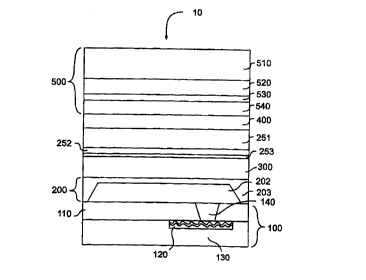
Fig. 1 discloses an organic light emitting device ("OLED") constructed
according to the
present invention. As embodied herein. OLED 10 of the present invention is
shown in Fig. 1 and
includes a substrate 100. Overlying the substrate 100 is a first conductor
200. Overlvin~ the first
conductor 200 is a second conductor 250. Sandwiched between the conductor
layers is a layer of
light emitting organic material 300. Overlying the conductors and the organic
material is a top cover
500. Between the second conductor 250 and the top cover S00 is a microcavitv
stack 400.
The substrate 100 is substantially planar and underlies and provides support
for the entire
OLED structure. The first and second conductors 200 and 250 function as either
electron injecting
or hole injecting layers. When the positive and negative charges from the
conductors meet in the
layer of organic material 300, light is emitted. OLED 10 of the present
invention may emit light
through either the top cover 500 or the substrate 100. The microcavity stack
400 functions to restrict
light emissions in directions parallel to the substrate i00 and also provides
increased light emissions
7
SUBSTITUTE SHEET (RULE 26)
CA 02294279 1999-12-22
WO 98/59528 PCT/US98/12694
toward the viewer in a direction perpendicular to the substrate. The top cover
X00 is typically
transparent and provides sealing and protection for the entire OLED.
The microcavity stack 400 restricts light emissions in directions parallel to
the planar
substrate 100 and provides increased light emissions toward the viewer. The
microcavitv stack 400
minimizes the channelling of light in the organic material 300. The
microcavity stack 400 also
directs upward, light which has been emitted in a near Lambertian manner. The
microcavitv stack
400 reduces the activation of neighboring pixels. and increases contrast and
color purity. y In the
preferred embodiment of the present invention, the microcavity stack 400 is
located over the organic
material 300. However, it is within the scope of the invention to include
microcavitv stacks both
above and below the organic material 300. While Fig. 1 shows microcavity stack
400 as a discrete
layer, it is within the scope of the present invention that the light
restricting functions of the stack
may be blended into the other elements of the OLED, e.g., the conductor
layers.
The microcavity stack 400 may comprise alternating layers of dielectric
material deposited
on top of one another. Each layer of dielectric material may be chosen for its
index of refraction.
The thicknesses of each layer of dielectric material may be calculated using
formulas commonly
available to those skilled in the area. The thickness of each layer depends
upon the number and type
of layers contained within the microcavity stack 400 and on the types of
organic material contained
within the Iight emitting organic material layer 300. The microcavity stack
400 and the organic
material layer 300 combine to narrow the bandwidth of the emitted light. Light
emissions may be
optimized by the microcavity stack 400 so that the majority of the emitted
light falls into the near
ultra violet or blue light range of the spectrum. The narrower range of
emitted light allows color
converters to be more efficient due to their narrower pick-up range.
The dielectric material may be evaporated at shallow angles to the planar
substrate 100 in
order to minimize pinhole density in the layers. An evaporation angle of
approximately 30 to 50
degrees is preferred. As an alternative to evaporation, sputter depositing may
also be used to reduce
pinhole densities. For better results. the deposition may be conducted while
the OLED structure is
rotating. Shallow angle evaporation and sputter deposition reduce the pinhole
density of the
microcavity stack 400 below values normally obtained using conventional 90
degree deposition
methods. Layers of transparent conductor may also be interspersed within the
microcavitv stack
400. For example. a layer of ITO may be mixed between the layers of dielectric
material. .
Zirconium oxide, silicon carbide. silicon oxide, silicon dioxide and lithium
flouride are
suitable dielectric materials for the layers which comprise the microcavity
stack 400. The preferred
8
SUBSTITUTE SHEET (RULE 26)
CA 02294279 1999-12-22
WO 98/59528 PCT/US98/12694
process of depositing the dielectric material is sputter or ion beam
deposition because these
processes result in increased densification and large differences of indices
of refraction between the
dielectric layers. Evaporation or low temperature CVD may also be utilized as
alternative processes.
The use of ion bombardment during deposition of the dielectric material has
many advantages. For
~ example, ion embodiment allows a single material may be used for the entire
microcavit~~ stack 400.
The stack 400 may be comprise alternating layers of densified and undensified
dielectric material
{e.g. SiO,). Alternatively, transparent conductive material (e.g. In,03) may
be densified by ion
bombardment and interspersed between layers of undensified dielectric material
(e.g. Zn0). Ion
bombardment also permits thin layers to used within the microcavity stack 400,
which may include
alternating layers of densified ZrO, and undensified SiO,.
The substrate 100 may underlie a plurality of different subpixels or cells 10.
The substrate
100 may be transparent if downward light emission is desired. The substrate
100 may be a planar
thin film transistor array contained on glass (similar to those typically used
for TFT-LCD notebook
displays). The thin film transistor array may be placed on foil or ceramic. As
an alternative to the
thin film transistor array, the planar substrate 100 may be formed from a
silicon integrated circuit
wafer. As shown in Fig. 2, the silicon substrate layer 130 may comprise
integrated circuits 120. The
integrated circuit 120 may be connected to the first conductor 200 by way of a
plug or via 140. The
plug 140 is contained within an insulator 110 (e.g. S10,). The via or plug 140
may be f fled with hot
aluminum or tungsten which is chemical vapor deposited ("CVD") and may be
planarized with the
surrounding insulator using chemical-mechanical polishing ("CMP").
The planar substrate 100 may include the matrix 800, shown in Fig. 8. The
matrix 800
includes matrix lines 801 or 802 which are capable of carrying current or
voltage pulses of selected
magnitudes. The pulses are provided to the matrix lines 801. 802 by drivers
{not shown). The
signals from the drivers pass to the conductors 200, 205 through one the
matrix lines 801 and 802,
the integrated circuit 120 and the plug 140. The signal from the driver
current of varying magnitude
to the conductors thereby determining whether or not each OLED or pixel cell.
is on, off or at some
intermediate gray level.
The matrix address lines 801. 802 may be sequenced so that Iight emissions are
constantly
changing. The viewer's eye integrates the emitted light to see images. The
drivers are optimally
built into the substrate 100 in order to save space and to minimize the number
of connections.
However, the drivers may be connected to the perimeter of the substrate 100
using TAB automated
bonding or other well known techniques. The drivers may provide merely on/off
signals for some
9
SUBSTITUTE SHEET (RULE 26)
CA 02294279 1999-12-22
WO 98/59528 PCT/US98/12694
applications such as word processing or spreadsheet. However, most sofrware
relies heavily upon
different gray levels for providing additional information to the viewer, and
therefore the drivers
must provide pulses of various magnitudes.
The drivers generate coded pulses for the active matrix 800. The pulses may be
coded using
~ either amplitude or pulse width modulation. For the electroIuminescent
display of the present
invention pulse width modulation is preferred because the sharpness of the
transfer function limits
the use of other methods. The pulse width modulated signal operates on a time
slice basis, where
the gray level is proportional to the amount of time the signal is applied to
the subpixels or cells.
Pulse width modulation is largely insensitive to the nonuniformities between
different cells or
OLEDs on the matrix. This insensitivity is a result of the signal switching
between the two extreme
points on the response curve. As a result. the use of a pulse width modulated
driver signal reduces
uniformity requirements and increases yield.
Ideally, the cells should be active almost continuously and refresh with a new
signal every
cycle (e.g., each cell is typically refreshed 10-75 times a second). A short
negative current pulse is
applied to a matrix line in order to refresh the cells connected to that line.
This refreshing process
permits the brightest light to be produced for any given voltage that is
applied to the conductors.
It is preferred that each OLED 10 include within its circuitry 120 a pair of
transistors and a capacitor
in order to achieve this end, although there are many acceptable substrate
circuit designs. Normally,
the image is presented to the viewer at all times except for during the brief
period when a cell is
being refreshed. In addition to improving OLED brightness. the refreshing
process improves the
OLED image retention immunity.
Fig. 3 discloses the first conductor 200 which may serve as either the cathode
or anode. The
first conductor 200 may be formed from materials such as MoSI,, WSh, Mo, Al.
or aluminum alloys
such as Al-2% Cu or Al+5% Ti. The first conductor 200 includes a conductor pad
202 which may
?5 be planarized with a surrounding dielectric 201. Silicon dioxide is a
preferred material for the
dielectric 201. Prior to planarization the conductor pad 202 is formed thicker
than required. A 500
nm amount of conductor is deposited followed by the deposition of 1,000 nm of
silicon dioxide. The
combined surface is chemically mechanically polished in order to leave a
planar surface of mixed
conductor and dielectric. The use of planarized conductor pads avoids edge
steps which can result
3 0 in thinning of the organic materials, and breakdown failures or broken
conductors during fabrication.
As shown in Fig. 4, the first conductor 200 comprises a conductor pad 202 with
tapered side
walls of at least 30 degrees or even more. The sloped conductor pad 202 is
surrounded by a
SUBSTITUTE SHEET (RULE 26) --
CA 02294279 1999-12-22
WO 98/59528 PCT/US98/12694
transition layer 203 capable of injecting holes or electrons. The transition
layer 203 may comprise
barium titanate or other high dielectric constant materials. The transition
layer 203 may also
comprise a dielectric material comprising ~ to 60 percent Cr and Si0 with or
without low work
function contaminants comprising alkali or alkaline metals such as Cs, Mg, Ba,
Sc or Li or alloys
or mixtures of these materials. The transition layer may also comprise other
organic or inorganic
injector materials such as CuPC. The slope of the pad 202 is achieved by
undercutting the edges.
The undercutting is achieved through resist or bilayer adhesion loss.
Alternatively, the undercutting
may be achieved by resist edge ablation during R.IE. As shown in Fig. 5, the
first conductor 200
may include both the transition layer 203 and dielectric layer 201. As
injection enhancement layer
(not shown) comprising Al+Li, Mg+Ag, or Pd. Pt or Au may be included over the
transition barrier
203. The injection enhancement layer improves the injection of holes or
electrons into the orsanic
material 300.
Fig. ~ discloses the layer of light emitting organic material 300 which
comprises three layers
310. 320 and 330. The arrangement of the layers is determined by the direction
of electron injection
into organic layer stack 300. When electrons are injected from the bottom of
the stack 300, layer
330 is preferentially Perylene doped BAIq; layer 320 is preferentially NPB;
and layer 310 is CuPc.
In the case of top electron injection, the composition of layers 310 and 330
would switch. The
preferred thicknesses for the CuPc, NPB and Perylene doped BAIq layers are i 5
nm, 60 nm, and 70
nm, respectively. The Perylene doped BAIq layer produces blue light. Blue to
ultraviolet light is
preferred to obtain full color displays using color conversion. White emitters
can be obtained from
either dysprosium dopant or a mixed layer emitter. Other colors. such as green
or white on black,
may also be used for monochrome or multicolored displays. As an alternative,
the layer of light
emitting organic material 300 may be comprise a single blended layer rather
than separate distinct
layers.
Overlying the light emitting organic material 300 is the second conductor 250.
As shown
in Fig. 3, the second conductor 250 includes a conductor layer 251 and a
transition layer 253. The
transition layer 253 is preferentially formed from either LiF or barium and
has a thickness of
approximately I 0 nms. In order to simplify fabrication, transition layers 253
and 203 are generally
composed of identical materials. The conductor layer 251 is formed by
depositing ITO to a
thickness of approximately 150 nms using long throw distance S-gun sputtering.
The S-gun sputter
deposition process will close off pinholes in-the conductor layer. Shadow
masks commonly used
11
SUBSTITUTE SHEET (RULE 26)
CA 02294279 1999-12-22
WO 98/59528 PCTNS98/12694
in the electronics industry may also be used to keep the transparent
conductors from depositing on
and shorting out exposed leads near the perimeter of the display.
An optional Better layer 252 may be located between the conductor layer 251
and the
transition layer 253. The Better layer 252 preferentially comprises
alternating layers of zinc oxide
~ and aluminum of approximately 1 nm each. The layers which make up the Better
layer 252 are
preferentially evaporated at shallow angles (e.g. 30 degrees). Pinholes in the
Better layer 252 may
be reduced by the shallow angle evaporation.
Overlying the second conductor 250 is the top cover 500. Top cover 500
includes a
protective cover glass 510, a color converter layer X20, and a barrier layer
540. The transparent
cover glass 510 preferentially is formed from silicon and has a thickness of
approximately .2 mm
thick. The cover glass 5I0 may overly the entire matrix 800.
As shown in Fig. 2, a barrier layer 540 overlies the microcavity stack 400.
The
barrier layer 540 comprises a layer of diamond-like amorphous carbon ("DLC")
or silicon carbide
(SiC), or in the case of top injecting OLEDs a cesium doped diamond-like
carbide composition (CsC
approximately 10% Cs and 90% C by molar ratio). DLC is a film consisting of
amorphous carbon,
which may include hydrogen, that is transparent and has a high refractive
index (>2). Such films
are typically deposited by laser ablation from graphite or plasma enhanced CVD
from a eas such as
methane with a small amount of oxygen. The barrier layer 540 acts a barrier to
residual moisture
within the OLED. The barrier layer 540 may also serve as a heat sink for heat
generated during light
emission. The barrier layer may also serve as a hole or electron injector.
When functioning as an
injector the barrier layer 540 is typically doped with Lithium or Palladium
for electron or hole
injection respectively.
As shown in Fig. 4, the barrier layer 540 underlies a sealing layer 530 and
overlies the
microcavity stack 400. The barrier layer 540 may be formed using either
shallow evaporation or
Plasma Enhanced Chemical Vapor Deposition ("PECVD"). The PECVD process may
include, for
example, inductively coupled plasma using a methane and diluted CFa source
plus an argon source.
Transparent inductively coupled plasma DLC films have low pinhole density and
a high index of
refraction making them easy to use when mutually combined with PECVD
evaporated or sputter
deposited silicon dioxide layers. Silicon carbide formed from PECVD or
evaporation may be used
in lieu of the DLC high index of refraction layers.
As shown in Fig. 7, the barrier layer 540 may comprise an upper DLC layer 541
and a lower
DLC layer 542. Multiple layers of Better material 545 and 546 may be formed
within the top Layer
12
SUBSTITUTE SHEET (RULE 26)
CA 02294279 1999-12-22
WO 98/59528 PCT/US98/12694
541. The Better material layers may be formed from calcium. magnesium.
titanium or aluminum in
alternation W th DLC or other dielectric materials S3N~, Si0 or SiO,. A
transparent conductor such
as Zn0 may be used in place of the transparent dielectric material in order to
provide added
conductivit<-. While, the structwe and materials set forth above are
preferred, the invention includes
the use of Better layer comprising any transparent material capable of
removing moisture.
A sealing layer 530 may be included between the barrier layer 540 and the
color converter
layer 520. The sealing layer 530 hermetically seals the OLED in order to
protect the device from
oxygen and moistwe. The sealing layer 530 is typically formed from a
commercially available heat
sink gel material. The gel material may be dried extensively by heating in a
high vacuum or by
mixing in a desiccant such as BaO. As an alternative, an ultraviolet light
cured epoxy, e.g. Acrylate,
may be used. Solvent containing adhesives are not recommended unless a totally
pinhole free cover
layer is produced. The sealing layer 530 may further comprise a mixture of
chemically active
materials such as finely powdered aluminum. calcium, magnesium or titanium for
moistwe removal.
Hermetic metal seals may also serve as the sealing layer 530. These metal
seals are commonly used
I S for hermetically packaging electronic equipment.
The sealing layer 530 may cover a plwaiity of OLEDs contained within a
display. The
sealing layer 530 is applied uniformly across the display to enswe no oxygen
or moisture is trapped
within the display. The sealing layer 530 is preferentially formed in a vacuum
environment. If a
vacuum environment is not available, the sealing layer 530 may be formed in an
inert gas
?0 environment such as nitrogen or argon. Adhesion in the sealing layer 530
may be induced by
selection of the proper sealing conditions. For example, exposing a display,
fabricated according
to the present invention, to a temperature of I00°C and a pressure of
~0 psi will normally induce
adhesion between the sealing gel and the surrounding layers. If the OLED is
sealed in a vacuum,
the resulting gap may be eliminated when air pressure is returned to the
exterior of the OLED.
25 The sealing layer 530 may include a heat adhesive perimeter seal (not
shown). The perimeter
seal may be used alone or in conjunction with the sealing layer 530 which
extends across the entire
display. Getter material such as finely divided Mg, Ba, Ca, Ai or Ti may be
mixed into the perimeter
seal for additional vapor collection. The perimeter seal typically comprises
an ultraviolet light caved
epoxy.
30 The color converter layer 520 may be formed by providing color conversion
dye materials -
above the barrier layer 540. The color conversion dye materials work with an
OLED emitter that
emits short wave length lights, for example blue, near ultraviolet, or
ultraviolet. The dye materials
13 -
SUBSTITUTE SHEET (RULE 26)
CA 02294279 1999-12-22
WO 98159528 PCT/US98/12694
generally comprise PPV based compounds or other fluorescent materials and are
commercially
available from many sources including, for example, Idemitsu Kosan
Corporation. The dye
materials absorb the short wave length flight and re-emit or fluoresce longer
wave length flight in
characteristic colors such as red or green. These color conversion dye
materials may be selected and
~ patterned on the cover glass X10 using conventional lithographic means. The
dye materials may be
used to create a full color CRT-like display with red, green and blue pixels.
The varying grey levels
available from the perimeter drivers and the active matrix may be used to
create intensity mixtures
of three primary colors and result in TV-like images. Blue converter dye
material may be used if
near-ultraviolet light emitting layers are used.
Full color displays may be displayed using color filters in lieu of converter
dye material. The
color filter may be used with a white light emitting organic layer 300. Blue
light emitting organic
material may be used with or without color filters. A further embodiment of
the color convener
layer X20. utilizes commercially available color wheels or pi-cells for color
conversion. All of these
techniques are commonly known in the industry.
The present invention also includes the use of black matrix or reflective
metal trenches 803
surrounding each subpixel or OLED 10. The black matrix or reflective metal
trenches 803, shown
in Fig. 8. help to minimize channeling in the small pitch pixels and improve
color purity. The black
matrix preferably comprises a mixture of co-evaporated 40 to 80% chromium and
silicon oxide. If
the OLED is to be used in a head wearable application, e.g. medical imaging,
night vision. or virtual
reality applications, it is preferred to use chromium or aluminum reflective
barriers. The chromium
or aluminum barriers may provide more light output while at the same time
controlling channeling.
It will be apparent to those skilled in the art that various modifications and
variations can be
made in the construction. co~guration. and/or operation of the present
invention without departing
from the scope or spirit of the invention. For example. in the embodiments
mentioned above,
various changes may be made to the composition of the organic material layers
without departing
from the scope and spirit of the invention. Further. it may be appropriate to
make additional
modifications or changes to microcavity structure without departing from the
scope of the invention.
Thus, it is intended that the present invention cover the modifications and
variations of the invention
provided they come within the scope of the appended claims and their
equivalents.
14
SUBSTITUTE SHEET (RULE 26)