Note: Descriptions are shown in the official language in which they were submitted.
CA 02295194 1999-12-17
WO 98/58415 PCT/US98/12645
CONTROLLED CONVERSION OF METAL, OXYFLUORIDES
INTO SUPERCONDUCTING OXIDES
Field of the Invention
This invention relates to highly oriented oxide superconducting films. The
invention further relates to processing of metal oxide- and metal fluoride-
containing
films into oxide superconductor films.
Background of the Invention
The discovery of superconducting ceramic oxides has fueled a tremendous
effort to fabricate these oxides into high performance films and coatings.
High
temperature superconducting (HTSC) film fabrication methods can be largely
divided into two areas: physical and chemical methods.
Physical methods include reactive evaporation, magnetron sputtering, e-
beam deposition and laser ablation. While physical deposition methods form
high
quality films, these deposition techniques typically have very slow formation
rates,
and require high vacuum environments so that they require expensive equipment.
In addition, the techniques are best suited for thin-film fabrication. For
these
reasons, physical deposition methods are extremely difficult to scale up to
multi-
meter lengths required for electrical or magnetic applications.
Chemical methods are largely based upon thermally activated chemical
reactions of precursor compounds during film formation. Chemical film
fabrication
methods involve a precursor which is deposited onto a substrate and later
transformed through thermal and chemical means to a film having the desired
composition and phase.
Films may be prepared using metalorganic chemical vapor deposition
(MOCVD), in which precursor films are deposited from metalorganic precursors
having a high vapor pressure. Metal-organic solution deposition (MOD)
processes
involve the deposition of a precursor film from a condensed phase precursor.
The
precursor film is then heated and converted into the final ceramic in a
separate heat
treatment.
MOD processes are widely used in industry for the deposition of ceramic
films. The process is ideally suited for the rapid, inexpensive deposition of
films
on large or continuous substrates. Other advantages of the MOD process include
CA 02295194 1999-12-17
WO 98/58415 PCT/US98/12b45
easy control of metal composition and homogeneity, short processing time, low
capital equipment cost and low precursor cost.
Typically in MOD processes, metal carboxylates of carboxylic acids,
alkoxides, or partially hydrolyzed alkoxides are dissolved in organic solvents
and
the resultant solution is deposited onto a substrate by dipping or spin
coating. The
precursor films produced by these coating processes are transformed into metal
compound-containing coatings by heat treatment, which most commonly includes a
series of distinct heating steps. While chemical methods represent versatile
and
inexpensive methods of film fabrication with potential for high speed
production,
they are very sensitive to secondary reactions which may be deleterious to
final
superconducting properties. For example, in the deposition of materials such
as
YBa,Cu;Oy, such processes are highly susceptible to the intermediate formation
of
barium carbonate (BaCO~). The stability of BaCO~ requires high processing
temperatures (>900 ' C) and extended processing times in order to decompose
the
barium carbonate and obtain the oxide superconductor. The extreme reaction
conditions result in film reaction with the substrate, poor texture of the
oxide
superconductor and incomplete formation of the oxide superconductor phase.
Chan et al. in Appl. Phys. Lett. 53(15):1443 (October 1988) discloses a
hybrid process, known as an ex sitar process, which includes the physical
deposition
of a precursor film which is then processed outside of the physical deposition
chamber by conventional chemicothermal processes. This PVD process (BaF, ex
situ process) separates the deposition and conversion steps. This process
involves
codeposition of CuO, Y20~, and BaF~ in the correct stoichiometric uniformly on
the
substrate. The film is then converted under conventional heating conditions
into
the oxide superconductor by annealing in the presence of water vapor. The
limitations of physical deposition methods described above remain, however.
Chan
et al observed that improved electrical performance was obtained by increasing
the
Po, and decreasing the PH,: during the anneal step.
Cima et al. in U.S. Patent No. 5,?31.074, report the MOD preparation of
Ba,YCu,O,_h (YBCO) oxide superconductor films having improved electrical
transport properties by MOD using metal trifluoroacetates on single crystal
SrTiO~
and LaAl03. The films of a thickness of about 0.1 pm possessed critical
transition
CA 02295194 1999-12-17
WO 98/58415 PCT/US98/12645
temperatures of about 90K and zero field critical current densities of greater
than
106 A/cm' at 77K.
In addition, the superconducting performance of epitaxial Ba,,YCu30~_x films
prepared using the process described in U.S. Patent No. 5,231,074 has been
found
to depend on film thickness. Electrical performance drops off dramatically as
film
thickness increases from 0.1 um to 1.0 um. Although thinner films have
routinely
been prepared with critical current densities greater than 106 A/cm',
application of
conventional chemical processing techniques in the preparation of films with a
thickness near 1.0 um never yielded results close to this level of
performance. For
example, a MOD process using metal trifluoroacetates has been used to prepare
thin (70-80 nm) YBa2Cu30y, (YBCO) films (where y is a value sufficient to
impart
superconductivity at temperatures of at least 77K) with T~ > 92K and J~ > 5 x
106
A/cm'' (77K, self field); however, it has not been possible to prepare much
thicker
films possessing similar properties. Indeed, prior to the development of the
processing techniques described in this patent application no solution-based
deposition process had been demonstrated that produced high J~ films with
thicknesses of over 0.5 um.
Thicker oxide superconductor coatings are needed in any application requiring
high current carrying capability such as power transmission and distribution
lines,
transformers, fault current limners, magnets, motors and generators. Thicker
oxide
superconducting films are desired to achieve a high engineering (or effective)
critical current (J~), that is, the total current carrying capability divided
by the total
cross sectional area of the conductor including the substrate.
It is desirable that oxide superconducting coatings greater than 0.5 um in
thickness have high critical current densities. There is a need for
fabrication
techniques which may be used to prepared these thick oxide superconductor
films
and coatings with superior electrical performances.
Summary of the Invention
It is an object of the invention to provide oxide superconductor films having
superior electrical properties.
3
CA 02295194 1999-12-17
WO 98/58415 PCTNS98/12645
It is a further object of the invention to provide oxide superconductor thick
films possessing high epitaxial alignment, and preferably c-axis epitaxial
alignment.
It is another object of the present invention to provide a method of
processing metal oxyfluoride precursor films into high quality oxide
superconductor
f lms.
It is a further object of the invention to provide a method of fabrication for
high quality relatively thick film oxide superconductors.
These and other objects of the invention are accomplished by controlling the
reaction kinetics for the conversion of the metal oxyfluoride into an oxide
superconductor, so that the rate of conversion takes place at a desired
controlled
rate. In particular, reaction conditions are selected which control the rate
of
consumption of BaF, and/or other metal fluorides and thus the HF evolution
rate
which among other effects permits sufficient time for the transport of HF from
the
film and which also reduces the HF concentration during the nucleation of the
oxide superconductor layer at the substrate/film interface. In particular, the
reaction temperature and the moisture content of the processing gas used in
the
reaction are controlled so as to adjust the conversion rate of the metal
oxyfluoride
into the oxide superconductor.
The present invention is applicable to any chemical processing system which
generates hydrogen fluoride upon hydrolysis in the preparation of a metal
oxide.
The presence of fluoride in the precursor film may have the additional
advantageous effect of doping the product oxide superconductor with fluorine
which had been demonstrated to increase its critical transition temperature
and,
hence, possibly its critical current density. The present invention may be
applied to
any film fabrication method which consumes barium fluorides or other metal
fluorides during deposition and processing.
By "metal oxyfluoride" as that term is used herein it is meant a composition
which contains metals, oxides and fluorides. The composition may include
cationic
metallic species bound to both oxygen and fluoride, e.g., MOxFv, where x and y
are
selected to satisfy metal valency, or it may include a mixture of metal oxides
and
metal fluorides. e.g., MO~ and MFG..
4
CA 02295194 1999-12-17
WO 98/58415 PCT/US98/12645
"Moisture content" as that term is used herein, refers to the vol% water
vapor contained in the processing gas used in the heat treatment of the
invention at
the point of its introduction into the furnace and may alternatively be
referred to as
PFizo or relative humidity (RH). Relative humidity may be referred to relative
to a
particular temperature since the capacity of the processing gas to contain
water
vapor is temperature-dependent. Moisture content is defined herein in terms of
relative humidity (RH), which represents the amount of water (%) in the
processing
gas relative to the amount of water in the processing gas at maximum capacity
(saturation) at the point of its introduction into the furnace at room
temperature
(RT).
By "coated conductor" as that term is used herein, it is meant, a
superconducting wire or tape in which the superconducting material is coated
on
the exterior of a substrate that forms the bulk of the wire or tape, or other
article.
In one aspect of the invention, a method for preparing an oxide
superconductor film includes providing a metal oxyfluoride film on a
substrate, said
metal oxyfluoride film having a thickness greater than or equal to about 0.5
p,m
and comprising the constituent metallic elements of an oxide superconductor in
substantially stoichiometric proportions; and converting the metal oxyfluoride
into
the oxide superconductor at a rate of conversion selected by adjusting a
reaction
parameter selected from the group consisting of temperature, PHZO and
combinations
thereof, such that an oxide superconductor film having a transport critical
current
density of greater than or equal to about 105 A/cm' at 77K, zero field is
obtained.
In another aspect of the invention, an oxide superconductor film is prepared
by providing a metal oxyfluoride film on a substrate, said metal oxyfluoride
film
comprising the constituent metallic elements of an oxide superconductor in
substantially stoichiometric proportions; and converting the metal oxyfluoride
into
the oxide superconductor in a processing gas having a moisture content of less
than
about 100% RH as determined at 25 °C.
In yet another aspect of the invention, an oxide superconductor film is
prepared by providing a metal oxyfluoride film, said metal oxyfluoride film
comprising the constituent metallic elements of an oxide superconductor in
substantially stoichiometric proportions; and converting the metal oxyfluoride
into
5
CA 02295194 1999-12-17
WO 98/58415 PCT/US98/12645
the oxide superconductor under reaction conditions selected to provide an
atmosphere above the substrate comprising an HF concentration at a level to
provide an oxide superconductor film having a transport critical current
density of
greater than or equal to about 10' A/cm'- at 77K, zero field.
In yet another aspect of the invention, an oxide superconductor film is
prepared by (a) providing a metal oxyfluoride film on a substrate, said metal
oxyfluoride film comprising the constituent metallic elements of an oxide
superconductor in substantially stoichiometric proportions; {b) converting the
metal
oxyfluoride into the oxide superconductor in a processing gas having a
moisture
content of less than 100% RH as determined at ?5 ° C for a time
sufficient to form
a layer of the oxide superconductor at the substrate/film interface; and (c)
completing conversion of the metal oxyfluoridc into the oxide superconductor
in a
processing gas having a moisture content greater than that in step (b). In
preferred
embodiments, a time sufficient to form a layer of the oxide superconductor at
the
substrate/film interface is in the range of about 15 minutes to about 2 hour.
In preferred embodiments, the moisture content comprises a relative
humidity less than about 95%, and preferably less than about 50%, and more
preferably less than about 1-3% as determined at 25 ' C. The substrate may
comprise a metal or a ceramic, wherein the ceramic is selected from the group
consisting of SrTiO~, LaAlO,, zirconia, preferably stabilized zirconia, Mg0
and
CeO~. The substrate may be substantially lattice-matched with the oxide
superconductor. In other preferred embodiments, the methods above further
comprise annealing the oxide superconductor film so as to oxygenate the oxide
superconductor.
In other preferred embodiments, conditions for converting the metal
oxyfluoride comprise heating the metal oxyfluoride film in a processing gas
having
a moisture content of less than about 95-100% RH as determined at 25 °
C and at a
temperature in the range of 700-900 ° C, or heating in an environment
where
oxygen content is selected to be as low as possible at a given temperature
while
still maintaining stability of the oxide superconductor phase.
In preferred embodiments, the metal oxyfluoride film is deposited using a
technique selected from the group consisting of MOD, MOCVD, reactive
6
CA 02295194 1999-12-17
WO 98/58415 PCT/US98/12645
evaporation, plasma spray, molecular beam epitaxy, laser ablation, ion-beam
sputtering and e-beam evaporation, or by depositing a metal trifluoroacetate
coating
onto the substrate and decomposing the metal trifluoroacetate coating to form
the
metal oxyfluoride film. Multiple layers may be applied. In preferred
embodiments, the oxide superconductor film preferably has a thickness of
greater
than or equal to 0.8 microns (~,m), and more preferably has a thickness of
greater
than or equal to 1.0 micron (~,m).
In another aspect of the invention, an oxide superconductor article is
provided
in which an oxide superconductor film has a thickness of greater than 0.~
microns
(gym) disposed on a substrate and the article has a transport critical current
density
(J~) of greater than or equal to about 105 A/cm' at 77K, in zero applied
magnetic
field.
In yet another aspect of the invention, a coated conductor article, is
provided
including a metallic core; a buffer layer disposed on the core; and an oxide
superconductor coating having a thickness greater than or equal to about 0.5
um,
said crystalline buffer layer substantially lattice-matched with the oxide
superconductor, said coated conductor exhibiting a critical current density of
greater
than or equal to about 105 A/cm' at 77K, self field.
The article may be further characterized in that the article possesses a
critical
transition temperature (T~) of greater than 92K. The article may be further
characterized in that the oxide superconductor comprises a sufficiently high
volume
percent of c-axis epitaxy so as to provide J~ values of equal to or greater
than 105
A/cm'- at 77K, in zero applied magnetic field. The article may be further
characterized in that the oxide superconductor comprises residual fluoride so
as to
provide T~ values greater than 92K.
In preferred embodiments, the oxide superconductor coating has a thickness
greater than or equal to about 0.8 ~,m and more preferably greater than or
equal to
about 1.0 um. In other preferred embodiments, the conductor has a critical
current
density of greater than or equal to about 106 A~'cm' at 77K, self field. In
other
preferred embodiments, the oxide superconductor is characterized by a high
degree
of c-axis epitaxy.
7
CA 02295194 1999-12-17
WO 98/58415 PCT/US98/12645
In yet another aspect of the invention, an oxide superconductor article is
provided including an oxide superconductor film having a thickness of greater
than
0.~ microns (~.m) disposed on a substrate, said oxide superconductor being
substantially c-axis epitaxially aligned.
Brief Description of the Drawing
The invention is described with reference to the Figures, which are presented
for the purpose of illustration only and are in no way limiting of the
invention, and
in which:
Figure 1 is a photomicrograph of the surface of a prior art oxide
superconductor
film;
Figure 2 is a photomicrograph of the surface of an oxide superconductor film
prepared according to the method of the invention;
Figure 3 is an illustration of a coated conductor of the invention;
Figure 4 is a flow diagram of the various fabrication processes which may be
used to prepare a coated conductor;
Figure 5 is a plot of Po, vs. 1000/T(K) demonstrating the CuZT/Cu- stability
line
for the formation of YBCO oxide superconductor;
Figure 6 are photomicrographs of oxide superconductor films processed to
obtain a low density (a) or a high density (b) film;
Figure 7 is a photomicrograph of an oxide superconductor film processed under
reduced temperatures;
Figure 8 is a plot of .I~ vs. film thickness for a variety of oxide
superconductor
films;
Figure 9 is a temperature-time profile of a typical low temperature heat
treatment for the MOD preparation of a metal oxyfluoride film;
Figures 10-14 are temperature-time profiles, based on key monitored values of
high temperature heat treatments for the MOD preparation of oxide
superconductor
films.
8
CA 02295194 1999-12-17
WO 98/58415 PCT/US98/12645
Detailed Description of the Invention
The present invention recognizes that improved electrical transport
properties of the invention may be achieved by processing the metal
oxyfluoride
film into an oxide superconductor under reaction conditions which control the
reaction kinetics of the process and the microstructure of the resultant oxide
film.
In particular, reaction conditions are selected which control the rate of
consumption
of BaF, and/or other metal fluorides and thus the HF evolution rate which
among
other effects permits sufficient time for the transport of HF from the film
and
which also reduces the HF concentration during the nucleation of the oxide
superconductor layer at the substrate/film interface.
The present invention further recognizes that it is possible to convert the
metal oxvf7uoride film into an oxide superconductor film under processing
conditions which will provide a highly oriented film with high critical
current
density. According to the method of the invention, temperature and P,j~o
conditions
are selected and applied as described herein during the step of conversion of
the
metal oxyfluoride into an oxide superconductor to provide an oxide
superconductor
film having a thickness of greater than or equal to 0.5 micron (~,m),
preferably
greater than or equal to 0.8 micron (p,m) and most preferably greater than or
equal
to 1.0 micron (gym), and a critical current density of at least 105 A/cm'' and
preferably at least 106 A/cmz. The oxide superconductor may be further
characterized as having substantial c-axis epitaxy, characterized by a
significant
absence of any a-axis aligned grains.
It has been observed that films which are described in the prior art possess
high angle grain boundaries. High angle grain boundaries represent 90 °
misoriented crystals on the film surface, which are deleterious to high
critical
current density. Critical current densities of films with many high angle
grain
boundaries are less than optimal because of the weak link behavior at each
local
grain boundary. These weak links are superconducting only when very small
amounts of current are passed through them. They become resistive, however,
when current is increased. High angle grain boundaries typically occur where
there
is roughly equal probability for both c-axis and a-axis orientation on the
substrate.
Thicker films, in particular, are prone to extended growth of a-axis oriented
grains,
9
CA 02295194 1999-12-17
WO 98/58415 PCT/US98/12645
which grow rapidly toward the film surface. The present invention provides a
film
where the amount of high angle grain boundaries is significantly reduced over
prior
art films and thus represents a significant improvement over prior art oxide
superconductor films.
The present invention provides oxide superconducting thick films, e.g.,
>0.5 dam which demonstrate high critical current densities. The inventive
oxide
superconductor films are characterized by high c-axis epitaxy of the oxide
superconductor grains with the substrate and by a high critical current
density, such
as greater than 105 A/cm', and preferably greater than about 10'' A/cm''. By c-
axis
epitaxy, as that term is used herein, it is meant that the principle axes of
the
substrate and film are arranged such that the c-axis of the oxide
superconductor is
normal to the substrate surface. The other principle axes of the oxide
superconductor, a and b (a only at high temperatures), are also aligned with
respect
to the principle axes of the substrate. Thus, within the oxide superconductor
layer,
the a, b and c axes are aligned. Similarly, by a-axis epitaxy, as that term is
used
herein, it is meant that the principle axes of the substrate and film are
arranged
such that the a-axis of the oxide superconductor is normal to the substrate
surface.
The other principle axes are aligned with substrate. In preferred embodiments,
the
films are characterized by a significant or majority of c-axis epitaxy and
little a-
axis epitaxy of the oxide grains. Note that c-axis epitaxy is defined for an
oxide
grain. The actual orientation of the oxide superconductor a and b axes with
respect
to the respective axes of the substrate may vary from grain to grain with no
significant effect on current carrying properties.
This is clearly demonstrated by comparison of the films of the prior art with
those of the present invention, as seen in Figures 1 and 2, respectively.
Figure 1 is
a photomicrograph of the surface of an 0.8 ~m thick oxide superconductor film
prepared according to prior art by heating a metal oxyfluoride film in a water-
saturated, 0.03% oxygen environment at 835 ° C. The film had a J~ of
1.6 x 10'~
A/cm'. The mosaic of a-axis epitaxial grains creates a network of 90 degree,
i.e.,
high angle grain boundaries, which are known to drastically decrease critical
current density of the film. The volume fraction of a-axis epitaxial grains in
the
film is substantial.
CA 02295194 1999-12-17
WO 98/58415 PCT/US98/12645
In contrast, the oxide superconductor films of the present invention exhibit
significantly less a-axis epitaxy of the oxide superconductor grains, as is
shown in
Figure 2. Figure 2 is a photomicrograph of a 1.0 micron (~,m) thick oxide
superconductor film of the invention which was heated in a 1.2% RH, 0.1% O,
environment at 785 ° C. This film is characterized by substantial c-
axis epitaxy of
the oxide superconductor crystalline grains normal to the substrate surface. c-
axis
epitaxy is demonstrated by the substantial absence of "edge-on" a-axis,
epitaxially-
aligned oxide grains which create a mosaic or basket weave pattern on the film
surface. Instead, c-axis epitaxy allows the plate-like grains to lie flat in
the plane
of the substrate surface. The film exhibits a critical transition temperature
of
~~reater than 90K, and a critical current density (J~) of at least 106 A/cm2.
Significantly, the film possesses these superconducting properties even with a
film
thickness of 1.0 um.
The invention includes superconducting coatings and films made with any
oxide superconductor, such as by way of example only, oxide superconductors of
the rare earth-barium-cuprate family of superconductors (ReBCO), where Re =
rare
earth elements, such as Y, Nd, Pr, the bismuth-strontium-calcium-cuprate
family of
superconductors (BSCCO), the thallium-strontium-calcium-barium-cuprate
(TBSCCO) and the mercury-barium-strontium-calcium-cuprate (HBSCCO) family
of superconductors. In preferred embodiments, the method is practiced using
the
oxide superconductor Ba,YCu30y, (YBCO), where y is a value sufficient to
impart
superconductivity at temperatures of at least 77K.
The substrate used in the preparation of the coated conductor article may be
any substrate which is not deleteriously affected by the processing conditions
and
chemicals used to prepare the oxide superconductor. The substrate may be of
any
shape or structure. It may be flat or three-dimensional and it may be in any
shape,
such as by way of example, in the form of tapes, wires, ribbons and sheets.
The
substrate may be single crystalline ceramic, or polycrystalline ceramic or
metal, or
other material. In demonstrated embodiments, the substrate is a ceramic
crystalline
material which is lattice matched with the oxide superconductor. Lattice-
matched
substrates are single crystal or polycrystalline ceramic materials having
similar
crystalline lattice constants as the oxide superconductor. Suitable substrates
11
CA 02295194 1999-12-17
WO 98/58415 PCT/US98/12645
include, but are in no way limited to, SrTi03, LaAl03, zirconia, preferably
stabilized zirconia, such as yttria-stabilized zirconia (YSZ), CeOZ, and MgO.
Other
suitable substrates include textured and untextured polycrystalline metal
substrates
of the appropriate lattice constant. In embodiments using metal substrates, it
may
be desirable to use a buffer layer between the substrate and the oxide
superconductor layer. Suitable buffer layers include but are not limited to,
zirconia, preferably IBAD YSZ, LaAlO;, SrTiO~, CeO, and MgO.
In another embodiment of the invention, coated conductor articles are
contemplated in which each layer imparts a desired property to the article.
For
instance, the base substrate may be a metallic substrate selected for
durability
and/or flexibility; and the base substrate may be coated with a buffer layer
which is
compatible with the oxide superconductor. This geometry is particularly well
suited for use as a coated superconductor wire or tape. With reference to
Figure 3,
a coated wire may comprise a metallic core 100. Suitable core materials
include,
but are not limited to steel, nickel, nickel alloys and alloys of copper, iron
and
molybdenum. The core optionally may be lattice-matched to the oxide
superconductor. Alternatively, the core may be deformation textured. The core
100 is coated with a buffer layer 102 which contains some degree of
crystallographic alignment and which is reasonably lattice-matched with the
oxide
superconductor. The buffer layer 102 has an epitaxial oxide superconductor
layer
104 deposited thereon. The oxide superconductor layer desirably has a
thickness in
the range of greater than or equal to 0.~ microns (um), preferably greater
than or
equal to 0.8 microns (um) and most preferably greater than or equal to 1.0
microns
(gym).
The coated conductor may be fabricated using the methods described herein
for the processing of a high quality thick film oxide superconductor layer.
The
coated conductor may be prepared using a variety of processing techniques,
such as
are set forth in Figure 4.
The preparation of oxide superconductor films according to the method of
the invention is described wish reference to YBCO; however, it is recognized
that
these principles may be applied to the manufacture of any oxide
superconductor.
In one embodiment, the oxide superconductor YBCO films of the present
invention
12
CA 02295194 1999-12-17
WO 98/58415 PCT/US98/12645
may be prepared using solutions of metal-trifluoroacetate (TFA) salts of the
constituent metals, Ba, Y and Cu. These salts are soluble in organic solvents
such
as esters, ethers and alcohols.
The TFA solution is deposited on the substrate. Coating may be
accomplished by many known coating methods, including but not limited to,
spmnmg, spraying, painting or dipping the substrate into the precursor
solution.
Oxide films may be fabricated on substrates having a varied geometry including
flat and three dimensional substrates, such as ribbons, wires, coil
geometries, and
patterned geometries. Substrates may be polycrystalline substrates or single
crystal
ceramic substrates lattice-matched to the oxide superconductor or they may be
non-
lattice matched. The present invention is particularly suited for the use of
lattice-
matched substrates in the formation of epitaxially-aligned oxide
superconductor
films. The nucleating oxide superconductor preferentially aligns its principle
axes
with the principle axes of the substrate to thereby obtain ordered crystal
growth and
orientation of the oxide film (epitaxy). Such order results in an oxide
superconductor in which each axis is substantially completely aligned. The
precursor may be applied in a single step or in multiple steps sufficient to
provide
an oxide superconductor film having a final thickness of at least 0.5 microns.
The TFA precursor is decomposed at low temperatures (e.g., <400 ' C) to
form an intermediate metal oxyfluoride compound. Fluoride is typically present
in
the film as barium fluoride (BaF2), although other metal fluorides which do
not
include barium may be present, such as by way of example, YF3. Because of the
similarity of the intermediate metal oxyfluoride film to physically deposited
films,
e.g., electron beam coevaporated films of BaFz, Y203, and Cu0 (Chan et al.,
supra), it is contemplated that metal oxyfluoride films prepared by PVD
processes
may also be treated in accordance to the method of the invention.
Metal oxyfluoride films maybe converted into the tetragonal YBCO phase
by reaction in a moist oxidizing atmosphere. The initial step is believed to
be the
reaction of the metal oxyfluoride precursor with water to form the
corresponding
metal oxides (CuO, Ba0 and Y~03) and HF~b~. The HF is removed from the film
by diffusion to the film surface and transport from the film in the processing
gas
flowing over the film. The final oxide superconductor film is desirably
13
CA 02295194 1999-12-17
WO 98/58415 PCT/US98/12645
substantially free from fluoride; however, it may be desirable that dopant
levels of
fluoride remain in the film. The presence of dopant levels of fluoride in
oxide
superconductors is known to increase the critical transition temperature and
critical
current density of the film. See, Doctoral Dissertation of Paul C. McIntyre,
Massachusetts Institute of Technology, June, 1993, entitled "Heteroeptiaxial
Growth
of Chemically Derived Ba~YCu30,_; Thin Films". Critical transition
temperatures
of greater than 92K have been observed.
Concurrent with and/or subsequent to the removal of the fluoride from the
film, the tetragonal YBCO phase forms and nucleates in the film. Thus, the
overall
reactions taking place in the film are shown in eqs (1) and {2),
BaF~ + H,O~~~ ----> Ba0 + 2HF~b~ ( 1 j
3Cu0 + %z Y~02 + 2Ba0 ___> yB~Cu306.s~ (2)
YBCO preferentially forms at the substrate surface, which enables its
alignment
with the substrate. The formation of YBCO preferentially occurs at a Poi and
temperature that is above the stability line 50 for the CuZ+/Cu+ reduction, as
shown
in Figure 5 (adapted from R. Beyers and B.T. Ahn, Superconducting Ceramics -
Proc. Xll Winter Meeting on Low Temperature Physics (Progress in High
Temperature Superconductivity, Vol. 31 ), eds. J.L. Heiras, L.E. Sansores,
A.A.
Valladares; World Scientific Publishing, Singapore, 1991; p. 55). If
conditions are
below this line, i.e., reducing conditions, Cu''T will be reduced and material
other
than YBCO will form. However, if conditions are too far above this line, e.g.,
too
oxidizing, then material other than YBCO ( 123 j will form such as YBCO ( 124)
or
YBCO (123.5). Additionally, processing near the stability line 50 may increase
the
amount of transient liquid present during nucleation and growth of YBCO (123)
and thereby result in films with higher density. (See, U.S. Patent No.
5,231,074.)
The YBCO phase nucleates and grows throughout the entire thickness of the
metal oxyfluoride film. This nucleation and growth process takes place after
or
simultaneous with the removal of fluoride from the film by a hydrolysis
reaction
which generates HF and BaO. In order for the resultant oxide film to maintain
an
epitaxy with the substrate, it is believed desirable for the YBCO phase first
to
14
CA 02295194 1999-12-17
WO 98/58415 PCT/US98/12645
nucleate at the film/substrate interface and for that transformation to
continue
upward towards the film surface.
The present invention recognizes that it is possible to convert the metal
oxyfluoride film into an oxide superconductor film under conditions which will
provide a highly oriented epitaxial film with high critical current density.
According to the method of the invention, temperature and P"Z~ conditions are
selected and applied as described herein during the step of conversion of the
metal
oxyfluoride into an oxide superconductor to provide an oxide superconductor
film
having a thickness of greater than or equal to O.Smicron (~,m), preferably
greater
than or equal to 0.8 micron (~,m) and most preferably greater than or equal to
I.0
micron (gym), and a critical current density of at least 105 A/cm~ and
preferably at
least 10G A/cm'. The oxide superconductor may be further characterized as
having
substantial c-axis epitaxial alignment, characterized by a signiftcant absence
of any
a-axis aligned grains.
The improved electrical transport properties of the invention are achieved by
processing the metal oxyfluoride film into an oxide superconductor under
reaction
conditions which control the reaction kinetics of the process and the
microstructure
of the resultant oxide film. In particular, reaction conditions are selected
which
control the rate of consumption of BaF, and/or other metal fluorides and thus
the
HF evolution rate which among other effects permits sufficient time for the
transport of HF from the film and which also reduces the HF concentration
during
the nucleation of the oxide superconductor layer at the substratc/film
interface.
The control of metal fluoride consumption in the film may have several
advantageous effects in the production of a highly aligned oxide
superconductor
film. A reduced consumption rate of BaF~ in a YBCO film, for example, will
reduce the presence of HF in the vicinity of the substrate and/or dissolved HF
in
the film itself. HF is reactive with many substrates and may etch the
substrate
surface. Etching can cause substrate roughening. Unevenness of the substrate
surface has been associated with the preferential growth of a-axis aligned
grains.
See, McIntyre et al. J. Crystal Growth 149:64 (1995). Further, the presence of
dissolved HF or fluoride ion in the film may deleteriously affect the
nucleation
kinetics of the oxide superconductor at the substrate. Therefore, a reduction
in the
CA 02295194 1999-12-17
WO 98/58415 PCT/US98/12645
HF concentration during conversion process may serve to reduce substrate
etching
and/or improve the nucleation of the oxide superconductor at the substrate
surface
to thereby improve the microstructure of the oxide superconductor.
Conventional processes have used the reaction temperature to control the
rate of BaF, consumption. The prior art stresses the importance of high
moisture
content in the processing gas during the removal of fluorine from the
oxyfluoride
films. A high PH,~ is expected to drive the hydrolysis reaction forward. Thus,
in
conventional processes, the moisture content during conversion of the
oxyfluoride
film into epitaxial oxide superconductor is kept as high as is practical, and
the
conversion rate is controlled by temperature. However, temperature affects
other
aspects of the conversion process such as the growth kinetics of the oriented
oxide
superconductor grains. The present invention has recognized that it is
possible to
use the moisture content of the processing gas as a rate controlling parameter
in
addition to temperature. Temperature may then be selected, for example, to
favor
the grov~-th of oriented, dense oxide superconductor films. The cooperative
selection of temperature and P,,,~ gives the process more flexibility and
provides a
route to higher quality films.
The present invention has identified moisture content as an additional
processing variable which may be regulated in order to manage reaction rates
during the conversion of metal oxyfluoride into oxide superconductor. Thus,
the
practitioner wishing to control the rate of BaF, consumption now has the
option of
either lowering the temperature or, for a given temperature, reducing the
amount of
water vapor in the processing gas. This additional option is particularly
valuable
since it is recognized that temperature plays a role in grain growth and film
density. Higher temperatures lead to more dense films, which typically exhibit
better current transport. Reaction at higher temperatures would not be
available in
the prior art for thick films (using process gas saturated with water vapor at
room
temperature) because an increase in temperature would result in an undesirable
rate
of BaF, consumption. For example, it has been observed that when processing
thick films under processing gas saturated with water vapor at room
temperature,
higher processing temperatures, e.g., 835 ° C for YBCO, produced f lms
which
were dense, but which contained an unacceptably high level of a-axis oriented
16
CA 02295194 1999-12-17
WO 98/58415 PCT/US98/12645
grains. Critical current density values of these films were poor, e.g., less
than
25,000 A/cm''.
The present invention permits the selection of reaction temperature so as to
obtain desirably dense films or other such consideration, while at the same
time
controlling the rate of BaF, by providing the additional processing variable
of
moisture content control. The present invention further identifies the
interdependency of the conversion process on the reaction temperature and the
water vapor pressure and provides guidance as to the relative levels of each
which
is desirable in order to obtain a thick film possessing superior electrical
properties.
In addition to selection of P"2~ and T, oxygen pressure (PoZ) is selected to
maintain processing conditions in a regime where YBCO is thermodynamically
stable. Details of the effects of varying oxygen levels in the processing
environment for a given temperature is given in further detail in the Doctoral
Dissertation of Paul C. McIntyre, Massachusetts Institute of Technology, June,
1993, entitled "Heteroepitaxy Growth of Chemically Derived Ba,YCu~O~_x Thin
Films", and in U.S. Patent No. 5,231,074, which are hereby incorporated by
reference. However, one of the advantages of the present invention is that
proper
selection of the temperature and water vapor pressure does not require that
the
reaction be carried out substantially close to the Cu2~/Cu+ stability line, as
had
previously been the case. Note for example in Figure 5, a one micron thick
YBCO
film was obtained well above the Cuz~/Cu' stability line having a critical
current
density of 10~ A/cm'. In general, it is desirable that a relative increase in
reaction
temperature is carried out in conjunction with a relative increase in oxygen
pressure. In preferred embodiments, the oxide superconductor is formed in a
temperature range of 700-900 °C, preferably in a temperature range of
700-835 °C,
and in 0.01-10 vol% O~. For example, YBCO may be formed at 835 ° C in
an
oxygen atmosphere of about 1.0% O,; and YBCO may be formed at 785 ° C
in an
oxygen atmosphere of about 0.1 % O,.
Thus, by way of example only and in accordance with the method of the
invention, a metal oxyfluoride film may be converted into a high quality YBCO
film of greater than 0.5 pm by heating at 785 ° C in a moist atmosphere
a relative
humidity of about 1.2% as determined at 25 ' C. Alternatively, a high quality
17
CA 02295194 1999-12-17
WO 98/58415 PCT/US98/12645
YBCO film with thicknesses greater than about 0.5 um may be obtained by
heating
at 835 ° C in a moist atmosphere having a relative humidity of about
0.6% at
25 ° C. Oxygen partial pressure is selected as described above to favor
thermodynamically the formation of the oxide superconductor.
Further, it has been observed that the temperature and moisture content
suitable to provide a superconducting thick film may vary with film thickness.
Thus for a given reaction temperature, an oxyfluoride film having a thickness
of
about 1.0 ~,m desirably is treated in a processing gas having a lower moisture
content than a comparable film having a thickness of about 0.5 ~,m. It is
contemplated that films with thicknesses considerably greater than 1.0 ~,m may
be
prepared with proper adjustment of the moisture content of the processing gas
to
lower levels.
The realization that the processing conditions used to form the oxide
superconductor should be selected so as to provide rate control over the
conversion
step is contrary to all teachings in the prior art, which advocate rapid
conversion of
the metal oxyfluoride film into Ba0 and HF. The prior art typically teaches
the
use of processing gas saturated with water vapor at room temperature
(typically
close to 100% RH at RT). In contrast, the present invention identifies an
additional processing variable, the moisture content in the processing gas,
which
may be reduced so as to allow for kinetic control of the conversion step.
The actual amount of moisture appropriate in the injected processing gas is
a function of the reaction temperature. At relatively higher processing
temperatures, the appropriate moisture content of the injected processing gas
is
relatively Less. The moisture content is measured at room temperature before
the
gas enters the heating chamber (furnace) containing the coated substrate.
Moisture
content of the processing gas at room temperature is typically less than 100%
RH,
preferably less than about 10% RH, and is more preferably less than about
2°io RH.
There may be a lower limit for the PN~~ of the system, as well, below which
the
reaction will not spontaneously proceed. The exact value may be determined by
reference to thermodynamic stability of the reactants or products.
Alternatively, it
may be determined empirically by lowering the P"~~ at a given temperature
until
18
CA 02295194 1999-12-17
WO 98/58415 PCT/US98/12645
the reaction no longer proceeds. Additionally, appropriate moisture levels may
be
well above such lower limits, since the processing time may be too long
otherwise.
An additional feature of the method of the invention is that control of BaF,
consumption also controls the rate of HF formation. Hydrogen fluoride is
generated during hydrolysis of metal fluorides, in particular barium fluoride,
in a
reaction which also generates the corresponding metal oxides. In one
embodiment
of the invention, HF concentration in the furnace above the substrate is
estimated to
be at or below 500 parts per trillion. One technique for maintaining the
partial
pressure of HF at a low level is to rapidly flush the processing gas through
the
furnace in which the coated sample is being heat treated. However, this may
result in a loss of control over other processing variables, such as furnace
and
sample temperature. A preferred approach for maintaining a low Pr,F is to
control
the rate of hydrolysis. One technique is to reduce the reaction temperature so
as to
slow down the overall reaction rate with the concomitant reduction in HF
production. Another technique is to control the amount of moisture in the
processing gas, the only significant source of water in the hydrolysis
process.
Thus, the hydrolysis reaction may be controlled, and hence the generation of
HF
may be regulated, by restricting the moisture content of the processing gas.
By
maintaining the water content of the processing gas below a predetermined
level
such that water is the rate limiting reagent, the rate of HF generation may be
regulated.
In one embodiment of the invention, the combination of a sufficiently low
moisture processing gas, sufficiently low reaction temperature, and high
enough
processing gas flow rate is used to ensure that partial pressure of HF is
estimated to
be in the hundreds of parts per trillion. The combination of low moisture
content
and low reaction temperature produce a slow reaction rate and therefore the
production of HF is also low. As stated above, processing gas moisture content
at
the inlet to the furnace is 1.2% and 0.6% at room temperature, respectively,
for
reaction temperatures of 785 ' C and 835 ° C, respectively. Processing
gas flow
rates may be about 3 L/min through a 5 cm ID quartz furnace tube giving a
space
velocity of about 150 cm/min; however, flow rates are expected to vary with
furnace size and configuration.
19
CA 02295194 1999-12-17
WO 98/58415 PCT/US98/12645
The exact conditions employed to obtain the final oxide superconductor film
are dependent upon the nature of the metalorganic precursors and the final
oxide
superconductor. In particular, the particular temperature, atmosphere, heating
rate,
etc., will be material-sensitive, however, exact conditions may be readily
determined by practice of the invention as described herein.
The method of the invention may be used to control the density of the
resultant oxide superconductor films. The growth kinetics of the oxide grains
improve with increasing temperature. Thus, high density films may be obtained
by
heating at high temperatures. Processing at higher temperatures may also
substantially increase the average grain size of the film. Because increasing
the
processing temperatures also increases the reaction rate of water with BaF,,
the
moisture level in the processing gas needs to be accordingly reduced in order
to
maintain the desired low rate of BaF~ consumption. The effect of these
processing
modifications are seen in comparing the photomicrographs of YBCO oxide
superconductor films of Figure 6. The film in Figure 6A was processed in 1.2%
RH(RTj moist nitrogen/oxygen atmosphere containing 0.1% O, at 785 ' C
(Example 2). The film in Figure 6B was processed in 0.6% RH(RT) moist
nitrogen/oxygen atmosphere containing 1.0% O, at 835 ° C (Example 3).
Both
films have a critical current density of about 10~ A/cm2 at one micron thick;
however, the microstructures differ significantly. The film of Figure 6A is
considerably more porous than that of Figure 6B. The increased grain growth at
higher reaction temperatures results in denser films.
According to the method of the invention, temperature may be lowered
sufficiently to permit the use of a water saturated processing gas, yet to
still obtain
oxide superconducting thick films having the superior electrical transport
properties
of the invention. The method of the invention may include processing at
reduced
temperatures. Because the lower reaction temperatures reduce reaction rate and
thus also the generation of HF, the reaction may be carried out with or
without
reduced moisture in the processing gas. As can be expected, especially in
light of
the comments immediately preceding regarding reaction temperature, reaction at
lower temperatures results in a more porous film. Figure 7 is a
photomicrograph
of a I ~:m thick YBCO oxide superconductor film processed at 700' C, in 0.01%
CA 02295194 1999-12-17
WO 98/58415 PCT/US98/12645
vol. O, processing gas saturated with moisture at room temperature (Example 1
j.
There is no noticeable a-axis epitaxy of the oxide superconductor grains;
however,
consistent with the observations above, the film is noticeably more porous
than
films processed at higher temperatures. Importantly, the film had a critical
current
density of 4.0 x 10⁵ A/cm', which exceeds prior art performance for oxide
superconductor films of comparable thickness.
Figure 8 is a plot of critical current density vs. film thickness for
Ba~YCu,O;_~ samples which were treated in a variety of ways. Solid data points
represent samples deposited on various lattice-matched substrates which were
prepared under processing gas saturated with moisture at RT. The electrical
performance of these conventionally processed samples drops off dramatically
for
samples with film thicknesses greater than 0.3 um (sec, Figure 8). Open data
points represent samples deposited on LaAIOj substrates which were processed
according to the method of the invention. These films exhibit critical current
densities greater than the prior art thick film samples, even in films with
thicknesses as great as one micron (see, Figure 8).
It is contemplated that any means of deposition of a metal oxyfluoride film
may be used in accordance with the invention. Chemical and physical deposition
techniques are contemplated as being within the scope of the invention, such
as but
not limited to, MOD, MOCVD, physical sputtering techniques, such as reactive
evaporation, magnetron sputtering, e-beam evaporation and laser ablation.
Thus,
metal oxyfluoride films may be deposited by MOD as described above, or they
may be deposited by MOCVD and then treated with the low moisture heat
treatment of invention. Typically, in an MOCVD process, high vapor pressure
sources of the constituent metal species, e.g., copper and yttrium and a metal
fluoride. e.g., barium fluoride or yttrium fluoride, are introduced into a
chemical
deposition chamber where they are deposited on the substrate. The as-formed
film
may be heat treated according to the method of the invention to form the oxide
superconductor.
It is further contemplated that a hybrid method including the ex situ
annealing of metal oxyfluoride films deposited by physical deposition methods,
may also be employed in the practice of the present invention. This allows for
the
21
CA 02295194 1999-12-17
WO 98/58415 PCT/US98/12645
separation of the film deposition step from the step of conversion into an
oxide
superconductor, providing better control of the individual steps and a
potential for
higher performance and productivity. Typically, independent sources of CuO,
Y,O~, and BaF, are used as targets in e-beam evaporation, with the deposit
rate
adjusted so as to deposit an amorphous film of the correct stoichiometry. The
film
may be heat treated according to the method of the invention, resulting in
removal
of fluorine by reaction with water and subsequent crystallization of the film
on an
epitaxial substrate. Further annealing in pure oxygen at lower temperature
produces the superconducting phase Ba,YCujO,~ (YBCO).
In another embodiment of the invention, a metal oxyfluoride film is
processed in a iow moisture environment for a time sufficient to nucleate and
grow
a thin layer of the oxide superconductor at the substrate/film interface. The
precise
thickness of this layer is not known, however, it is estimated to be on the
order to
tenth (0. I ) to hundredths (0.01 ) of a micron thick. Thereafter, the amount
of
water vapor in the processing gas is increased and is preferably increased up
to the
saturation point. The process is continued until conversion of the metal
oxyfluoride
into the oxide superconductor is complete. While not being bound by any
particular mode of operation, the presence of the initial oxide
superconducting layer
may prevent substrate etching by any HF retained in the film itself and/or
above
the substrate. Alternatively, the reduced HF content within the oxyfluoride
film
may favor c-axis orientation. Once an oriented layer is formed on the
substrate,
orientation of the subsequent oxide superconductor may not be dependent upon
HF
concentration. For a low moisture heat treatment at 835 °C, 1.0% O, and
0.6% RH
at RT, it has been observed that a sufficient layer is formed by treating for
15 min.
to one hour (Examples 4 and 5). It is contemplated that the heat treatment may
be
longer or shorter, dependent upon other reaction conditions, most notably
temperature; however, in preferred embodiments, the combined heating time for
the
first low moisture step and the second high moisture step typically is less
than the
time required when using solely a low moisture heat treatment.
Regardless of the mode of operation and as demonstrated in Examples 4 and
5, once the initial layer is formed, the water content of the processing gas
may be
increased without harm to the forming oxide superconductor film. Use of the
low
CA 02295194 1999-12-17
WO 98/58415 PCT/US98/12645
moisture process only to form an oxide superconductor initial layer may be
desirable for reducing processing time due to the rate limiting nature of the
low
moisture process of the invention.
Investigations by the present applicants have established that a surprising
amount of hydrogen fluoride is desorbed from the furnace glassware under
conventional processing conditions. This hydrogen fluoride had presumably been
adsorbed by the furnace glassware during earlier film processing experiments.
It is
not readily apparent whether improved electrical performance is the result of
a
decreased rate of HF formation, BaF2 consumption or Ba0 formation, or because
the PH,: of the system is reduced. The rate of hydrolysis and the rate of
oxide
superconductor formation may depend on many factors, such as mass transfer
limitation within the film, BaF2 crystallite size, etc.
While not being bound to any particular theory of operation, it is
hypothesized that evolution of HF by the furnace glassware exacerbates
substrate
etching which is detrimental to film quality. Many substrates suitable for
growing
oxide superconductor films are susceptible to HF etching. The higher the HF
concentration in the furnace, the greater the substrate etching. HF etching of
the
substrate causes surface defects or steps which create more sites for a-axis
growth
on the substrate (See, McIntyre et al., supra). This hypothesis is consistent
with
many of the observed phenomena of the process.
The hypothesis may explain why prior to the invention described herein thin
films of high superconducting quality could be produced while fabrication of
thicker films was problematic. In the fabrication of thin films, much less
metal
oxyfluoride is deposited on the substrate surface and, therefore, the
hydrolysis
reaction generates much less HF. In addition, the diffusion length for the HF
through a thicker metal oxyfluoride layer is greater than through a thinner
layer.
Less HF in the furnace atmosphere and/or in the oxyfluoride film means less
surface etching and, hence, less a-axis oxide grain growth. Thicker films
under
uncontrolled reaction conditions will generate a larger amount of HF and
retain a
given amount for a longer time which can significantly etch substrate surface.
It
has previously been observed that surface defects promote undesirable a-axis
epitaxial oxide grain growth.
23
CA 02295194 1999-12-17
WO 98/58415 PCT/US98/12645
The hypothesis further explains the substrate dependency observed when
fabricating films with the conventional process. Note that the performance of
conventionally produced films on SrTiO~ substrates is more adversely affected
by
thickness than conventionally produced films on LaAl03 substrates (Figure 8).
Some substrates, e.g., SrTiO,, are expected to be more sensitive to HF etching
or
reaction than other substrates, e.g., LaAIO~. Thus, during conventional
processing
where significant amounts of HF are being generated, those substrates that are
particularly sensitive to HF etch will degenerate more significantly than
those that
are less sensitive. In contrast, it is expected that HF etching of the
substrate would
be considerably lessened in processing according to the present invention,
since HF
partial pressures are being maintained at lower levels during and prior to
nucleation
of the superconducting oxide at the substrate film interface.
The invention may be described by way of the following examples which
are presented for the purposes of illustration and which are in no way
intended to
be limiting of the invention, the full scope of which is set forth in the
claims which
follow.
Prior to describing the details of each example, a general description of the
sample preparation, processing equipment and protocol, and heat treatments
used is
given. This general description applies to all the examples.
Sample preparation. Samples were prepared by coating polished single
crystal LaAlO, substrates with a liquid solution of the mixed-metal
trifluoroacetates
(Ba, Y. and Cu in the relative metal molar concentrations of 2, 1, and 3,
respectively) and methanol.
The liquid solution for spin coating was prepared by reacting the metal (Ba,
Y, Cu) acetates and trifluoroacetic acid in water, drying the product to a
semisolid
(glassy) state and then redissolving the product in methanol. Stoichiometric
quantities of the metal acetates and trifluoroacetic acid were used,
presumably
resulting in final solution of mixed-metal trifluoroacetates in methanol in
which the
metal ratio Ba:Y:Cu is 2:1:3.
The substrates were obtained by sectioning larger LaAlO; single crystal
substrates with a diamond wire saw. The substrates were 0.020" thick and
typically
24
CA 02295194 1999-12-17
WO 98/58415 PCT/US98/12645
approx. 1/4" x 1/4" although it is clear that any size substrate, even long
wires or
tapes will benefit from the method of the invention.
Prior to spin coating, the substrates were cleaned chemically and
mechanically. They were ultrasonically cleaned in chloroform, acetone and
methanol, respectively, and then wiped with a low lint tissue moistened with
methanol. The substrates were examined optically under SOX magnification after
wiping. Rewiping was performed as necessary to remove any residual dust or
contamination. If repeated wiping did not succeed in removing contamination,
the
entire cleaning process was repeated.
The coating was obtained by spin coating using a photoresist spin water in
a particulate containment hood under conditions in which the temperature in
the
hood was close to room temperature and the humidity in the hood was kept
substantially below 50% RH. The unfired films were observed to quickly dewet
from the substrate material when exposed to moist room temperature air (e.g.,
greater than SO% RH).
The samples were then loaded into the furnace and placed into the
processing zone. The sample loading procedure exposed the samples to
unfiltered
room air for only a few seconds.
Processing equipment and protocol. The furnace architecture for all the
processing steps used to convert the spun films into the superconducting films
was
a horizontal split type. The architecture used for the processing step that
converted
spun films into oxyfluoride films incorporated precise temperature control
tailored
for relatively low temperature parts of the heat treatment.
The temperature controlled sections of the main furnace tube, tube liner and
furnace furniture were all fabricated from silica glass. The furnace furniture
consisted of a tube with a D-shaped cross-section ("D-tube") having a movable
silica plate on top.
Furnace gas flow rate control for the processing step that converted spun
films into oxyfluoride films was provided by using a manually controlled flow
meter and regulated gas pressure. Dry and moist Ultra High Purity (UHP)
molecular oxygen gas was used. The injected furnace gas was switched from dry
to moist during an initial fast heating ramp rate period. The switch to moist
gas
CA 02295194 1999-12-17
WO 98/58415 PCT/US98/12645
was made after approximately 13 minutes into the initial fast heat up period.
A
volumetric flow rate of 10 t 1 scfh was used for the dry molecular oxygen, and
a
volumetric flow rate of 8 t 1 scfh was used for the moist molecular oxygen.
The
diameter of the main furnace tube was 5 cm. The distance from the gas inlet to
the
processing zone was approximately 1.1 m. Moist furnace gas was obtained by
passing the furnace gas through purified water at room temperature, until
saturated
(in the range of approximately 95-100% RH at RT) prior to injection into the
processing environment.
Furnace furniture temperature was monitored with a stainless steel sheathed
thermocouple probe (0.03?" diameter) with the probe tip placed between the
sample
positions. This temperature measurement probe was an ungrounded type K
thermocouple probe (purchased from Omega Co.). The probe was positioned in
direct contact with the furnace furniture, on the side of the furniture's
movable
plate upon which samples were placed.
The furnace architecture for the part of the processing that converted the
oxyfluoride films into the oxide films was similar to the system described
above,
with the following exceptions. The temperature control performance was
tailored
for better high temperature control and the length of the tube upstream of the
sample was approximately 0.6m. Also the themocouple used for measuring the
sample temperature was 0.062" in diameter and Inconel sheathed. It was
positioned with the tip near but downstream of the sample positions in a
closed end
high purity A1,03 protection tube which was in direct contact with the furnace
furniture, on the side of the furniture's movable plate upon which samples
were
placed. Low P~~ furnace gas for the high temperature heat treatments were
prepared using electronically controlled mass flow controllers to mix
ultrahigh-
purity nitrogen with analyzed oxygen/nitrogen gas mixtures prior to injection
into
the processing environment. The total flow rate of gas through the furnace was
kept at 3.0 L/min., for the low Poi portion of the heat treatment. A flow rate
of 4
scfh was used for the 100% O, portion of the heat treatment. This flow rate
was
provided using a manually controlled flow meter and regulated gas pressure.
Heat treatment. The samples were heated treated in two stages. Metal
oxyfluoride films were produced by heating according to the heat treatment
profile
?6
CA 02295194 1999-12-17
WO 98/58415 PCT/US98/12645
shown in Figure 9. Although the switch from dry to moist oxygen was done at
about 13 minutes into the initial heat up, due to a lag in the heat up of the
furnace
furniture with respect to the heat up of the furnace heating elements, the
sample
temperature was only approximately 50 ' C at that point. The moist gas was
used to
suppress volatilization of copper trifluoroacetate; however, the unfired films
quickly
dewet from the substrate when exposed to the moist furnace gas at a low
temperature. Switching from the dry to the moist processing environment when
the
furnace furniture was approximately SO ° C was found to sufficiently
address both
of these issues, given the equipment and process design used. The flow of
humid
oxygen was maintained until the temperature reached the peak value for this
part of
the process (approximately 400 ' Cj, at which point the furnace power and the
flow
of gas were shut off. The furnace was then allowed to cool with the samples in
the
stagnant, humid oxygen.
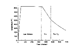
The oxyfluoride films obtained from decomposition of the metal
trifluoroacetates were subsequently converted to BazYCu~O~~ by annealing at
temperatures in the range of 700 - 835 ' C in environments of controlled Poz
and
PHZO~ Details of processes for this subsequent conversion to Ba zYCu ~J ~_X
are given
in the following examples.
Example 1. This experiment describes the preparation of YBCO oxide
superconductor thick films from TFA precursors by using a relatively low
annealing temperature.
During this heat treatment (see Figure 10), dry, 0.01 % OZ gas mixture was
injected into the processing environment for the first three minutes of the
initial
temperature ramp up. Due to a Iag in the heat up of the furnace furniture with
respect to the heat up of the furnace heating elements, the sample temperature
was
still approximately room temperature at this point. Then the incoming gas was
switched to high moisture (in the range of approximately 95-100% RH at RT)
0.01 % Oz gas mixture. The humid, low P~,2 atmosphere was passed over the
sample throughout the remainder of the heat up and high temperature hold until
the last 10 minutes of the high temperature hold. The hold temperature was 700
°C
(rounded to the nearest 10 °C and with an initial overshoot of
approximately 10
°C). With 10 minutes remaining in the high temperature anneal, flow of
the dry
27
. .. ..... . .__ .. .. . W....~-.~. _ . ..w .°.......r.~ ....
...~._..._.._ . _.~.~. .~-.. _.. ...~....___ __
CA 02295194 1999-12-17
WO 98/58415 PCT/US98/12645
low P~~ gas mixture resumed. Following this dry purge at the annealing
temperature, the dry gas mixture flow was maintained as the samples cooled
until
the furnace furniture temperature was about 525 ° C, at which point the
flow was
switched to dry oxygen and the furnace was allowed to cool to room
temperature.
The sample obtained by this procedure had a 1.0 micron thick oxide
superconductor layer. Critical current density was measured using a 1 uV/ cm
criterion. The film possessed a critical current density (J~) of 0.4 x 10~
A/cm'.
Example 2. This experiment describes the preparation of YBCO oxide
superconductor thick films from TFA precursors by annealing in low moisture.
Low moisture gas was prepared by precisely blending high moisture gas with dry
gas using a high precision manual flow meter just prior to injection into the
processing environment.
The sample preparation and furnace apparatus was as described in Example
1, with the following modifications. Low moisture 0.1% Oz gas mixture was
injected from the start of the heat treatment until the last 10 min. at the
annealing
temperature, at which point dry 0.1 % O, gas mixture was injected. The
moisture
level of the humid gas mixture used was 1.2% RH at RT. The annealing
temperature was 785 ' C (rounded to the nearest 5 °C and with no
substantial
overshoot). This heat treatment for this example is shown in Figure 11. The
film
possessed a critical current density (J~) of 1.1 x 10⁶ A/cmz.
Example 3. This experiment also describes the preparation of YBCO oxide
superconductor thick films from TFA precursors by annealing in low moisture.
The sample preparation, furnace apparatus, and heat treatment was as
described in Example 2, with the following modifications. The annealing
temperature was 835 ' C (rounded to the nearest 5 °C and with no
substantial
overshoot), the moisture level was 0.6% RH at RT, and the P~~ level was 1.0%.
The
heat treatment for this example is shown in Figure 12. The film possessed a
critical
current density (J~) of 1.0 x 10⁶ A/cm~.
Example 4. This experiment describes the preparation of YBCO oxide
superconductor thick films using the formation of an oxide superconductor
passivating layer at the substrate to reduce processing time.
28
CA 02295194 1999-12-17
WO 98/58415 PCT/US98/12645
Sample preparation. furnace apparatus, and heat treatment as described in
Example 3, with the following modifications. The high temperature anneal
consisted
of I hr. at the low moisture level (0.6% RH at RT), then 1 hr. at the high
moisture
level (in the range of about 9~-100% RH at RTj and then the 10 minute dry
purge.
The heat treatment for this example is shown in Figure I 3. The film possessed
a
critical current density (J~j of 0.9 x 1 O6 A/cm'.
Example 5. This experiment describes the preparation of YBCO oxide
superconductor thick films using the formation of a oxide superconductor
passivating
layer at the substrate to reduce processing time.
Sample preparation, furnace apparatus, and heat treatment was as described in
Example 3, with the following modifications. The high temperature anneal
consisted
of 1 ~ min. at the low moisture level (0.6% RH at RTj, then 45 min. at the
high
moisture level (in the range of approximately 95 - 100% RH at RTj and then the
10
minute dry purge. The heat treatment for this example is shown in Figure 14.
The
film possessed a critical current density (J~j of 0.~ x 10~ A/cm~.
Example 6. This example describes the treatment of a metal oxyfluoride film
prepared using conventional PVD methods through heat treatment according to
the
W vention.
Films may be prepared by coevaporation of Y, BaF, and Cu from three
separate sources. The barium fluoride and yttrium may be evaporated using
electron
beam guns and the copper may be evaporated using a resistively heated source.
The
three sources may be in triangular configuration with respect to one another
and the
rates from the sources may be monitored. The background pressure may be about
2 x
10-6 torr and during deposition oxygen is introduced into the chamber to
deposit an
oxyfluoride film resulting in a chamber pressure of about 5 x 10⁻⁵ torn. The
deposition
may be continued until a film of desired thickness is obtained.
The thus obtained metal oxyfluoride film may be treated as described in
Examples 1-6 to obtain an oxide superconducting film.
What is claimed is:
29