Note: Descriptions are shown in the official language in which they were submitted.
CA 02295225 1999-12-23
WO 99100855 PCT/US98/13535
METHOD AND SYSTEM FOR DETECTING MATERIAL
USING PIEZOELECTRIC RESONATORS
FIELD OF THE INVENTION
This invention relates generally to sensors for
detecting small quantities of materials, and more
particularly to material sensors based on piezoelectric
resonators.
BACKGROUND OF THE INVENTION
Resonators based on piezoelectric properties of
materials have been used in many important applications.
For instance, quartz crystal resonators are widely used
as frequency control elements in oscillator circuits
found in many devices such as computers and watches.
They are also used as bulk-acoustic wave filters in a
variety of circuits for frequency selection purposes.
One important application of piezoelectric
resonators is in detecting very small quantities of
materials. Piezoelectric resonators used as sensors in
such applications are sometimes called "micro-balances."
A piezoelectric resonator is typically constructed as a
thin planar layer of crystalline piezoelectric material
sandwiched between two electrode layers. When used as a
sensor, the resonator is exposed to the material being
detected to allow the material to bind on a surface of
the resonator.
The conventional way of detecting the amount of
the material bound on the surface of a sensing resonator
is to operate the resonator as an oscillator at its
resonant frequency. As the material being detected
binds on the resonator surface, the oscillation
- 30 frequency of the resonator is reduced. The change in
the oscillation frequency of the resonator, presumably
caused by the binding of the material on the resonator
surface, is measured and used to calculate the amount of
the material bound on the resonator or the rate at which
the material accumulates on the resonator surface.
SUBSTITUTE SHEET (RULE 26)
CA 02295225 1999-12-23
WO 99/00855 PCTIUS98/13535
2
The sensitivity of a piezoelectric resonator as a
material sensor is typically proportional to its
resonance frequency. Thus, the sensitivities of
material sensors based on the popular quartz crystal
resonators are limited by their relatively low
oscillating frequencies, which typically range from
several MHz to about 100 MHz. The recent development of
thin-film resonator (TFR) technology has produced
sensors with significantly improved sensitivities. A
thin-film resonator is formed by depositing a thin film
of piezoelectric material, such as A1N or ZnO, on a
substrate. Due to the small thickness of the
piezoelectric layer in a thin-film resonator, which is
on the order of several microns (um), the resonant
frequency of the thin-film resonator is on the order of
1 GHz or higher. The high resonant frequencies and the
corresponding high sensitivities make thin-film
resonators useful for material sensing applications.
The conventional method of detecting material by
measuring a change in the oscillation frequency of the
sensing resonator requires the incorporation of the
sensing resonator in an oscillator circuit to drive the
sensing resonator into oscillation. To obtain accurate
measurement results, the oscillator circuit has to be
stable and frequency matched to the resonant frequency
of the sensing resonator. This requirement, however, is
difficult to satisfy in practice. Many applications use
sensors of a disposable type, i.e., sensors have to be
replaced from time to time. In such a case, the same
electronics will be used with many sensing resonators.
Nevertheless, due to variations in the fabrication
process, the sensing resonators may have significantly
different resonant characteristics. For instance, the
non-uniformity in the deposition thickness of a
piezoelectric layer deposited across a substrate can
cause the resonance frequencies of thin-film resonators
from the same production batch to vary significantly.
SUBSTITUTE SHEET (RULE 26)
CA 02295225 1999-12-23
WO 99/00855 PCTlLIS98/13535
3
As a result, a non-adjustable oscillator circuit is
incapable of effectively driving all of the sensing
resonators into oscillation. It is possible to use
external tuning elements to fine tune an oscillator
circuit to match the resonant characteristics of
individual sensing resonators. The use of tuning
elements, however, can significantly increase
undesirable phase noise. Moreover, fine tuning the
oscillator circuit to match the sensing resonators is
not feasible in practice for field applications.
Another significant disadvantage of the
conventional approach is the difficulty in separating
the real signal from spurious environmental effects.
During material detection, a sensing resonator is often
exposed to different environmental conditions that also
tend to alter the oscillation frequency of the
resonator. It is often difficult to isolate the
frequency change caused by the material detected from
the frequency changes caused by various environmental
conditions.
SUMMARY OF THE INVENTION
In view of the foregoing, it is a primary object of
the present invention to provide a method and system for
detecting materials using piezoelectric resonators that
effectively avoids the difficulties in matching
oscillator circuits to the resonant characteristics of
individual sensing resonators.
It is a resultant object of the invention to
provide a method and system of detecting material with
piezoelectric resonators that does not require the
incorporation of sensing resonators in oscillator
circuits.
It is a related object of the invention to provide
a method and system for detecting material with
piezoelectric resonators that does not use the
conventional approach of incorporating the sensing
SUBSTITUTE SHEET (RULE 26)
CA 02295225 1999-12-23
WO 99/00855 PCT/US98/13535
4
resonators into oscillator,circuits and is capable of
providing high measurement sensitivity, stability, and
ease of operation.
It is a further related object of the present
invention to provide a method and system for detecting
materials with piezoelectric resonators that does not
require the use of the resonators in oscillator circuits
and operates in a way that allows effective separation
of the desired signal from environmental effects.
It is an object of the invention to provide a
piezoelectric sensing device suitable for a method and
system for detecting materials that does not require the
use of sensing resonators in oscillator circuits.
In accordance with these and other objects of the
invention, there is provided a method and system for
detecting material using a sensing resonator that
measures a change in insertion phase shift of the
resonator caused by the binding of the material being
detected on a surface of the resonator. An input
electrical signal having a frequency within a resonance
band of the piezoelectric resonator is coupled to and
transmitted through the resonator to generate an output
electrical signal which is phase-shifted from the input
signal due to the insertion of the resonator in the
signal path. The insertion phase shift is altered when
the material being detected binds on the resonator
surface. The output electrical signal received from the
piezoelectric resonator is analyzed to determine the
change in insertion phase shift caused by the binding of
the material on the resonator surface. The measured
change in insertion phase shift provides quantitative
information regarding the material bound to the
resonator surface.
It is a feature of the present invention to detect
material binding on a sensing resonator by measuring the
change in insertion phase shift, in contrast to the
conventional approach of operating the sensing resonator
SUBSTITUTE SHEET (RULE 26)
CA 02295225 1999-12-23
WO 99/00855 PCT/US98/13535
as an oscillator and detecting a change in the
oscillation frequency. Thus, the need for tuned
oscillator circuits is entirely eliminated, and
therewith the problem of matching oscillator circuits
5 with different sensing resonators. One of the important
advantages of the phase shift detection according to the
invention is that the input electrical signal is kept at
a constant frequency during the measurement. The
constant frequency of the input signal provides a
baseline of the measurement, and there is no longer the
need to follow an ever changing oscillation frequency as
in the conventional method.
Another advantage of the phase detection according
to the invention is the simplification of the
electronics for the sensing system. Because the input
signal is kept constant during measurement, simple and
inexpensive signal sources with adjustable output
frequencies, such as frequency synthesizers, can be
used.
Another significant advantage of the phase
detection approach is that one signal source can be used
to provide input signals simultaneously to multiple
resonators. As a result, a reference resonator may be
used in conjunction with a sensing resonator to
effectively separate environmental effects from the
phase shift change caused by the binding of the material
being detected on the sensing resonator.
The phase detection approach of the invention can
be advantageously used with different types of sensing
resonators in different configurations. For instance,
both the conventional quartz crystal resonators and the
newer thin-film resonators can be used as sensors, and
the sensing resonator may be configured as a one-port or
two-port device. Depending on the applications, the
resonators in the sensor may operate in longitudinal or
shear modes.
In a particularly advantageous embodiment, a thin-
SUBSTITUTE SHEET (RULE 26)
CA 02295225 1999-12-23
WO 99/00855 PCT/US98/13535
6
film sensing device includes a reference resonator and
at least one sensing resonator monolithically formed on
a substrate. The input electrical signal is coupled to
the electrodes of the reference and sensing resonators
via a transmission line and a power divider. The close
proximity of the reference and sensing resonators allows
the resonators to be fabricated with closely matched
resonant characteristics, which allow effective
cancellation of environmental effects during material
sensing operations.
Other objects and advantages will become apparent
with reference to the following detailed description
when taken in conjunction with the drawings in which:
BRIEF DESCRIPTION OF THE DRAWINGS
FIGURES lA and 1B are schematic diagrams
illustrating the operational principles of the
invention;
FIG. 2 is a schematic diagram of a material sensing
system having a one-port resonator as a sensor;
FIG. 3 is a schematic diagram of a material sensing
system having a one-port sensing resonator and a one-
port reference resonator;
FIG. 4 is a schematic diagram of a material sensing
system with two-port sensing and reference resonators;
FIGS. 5A and 5B are schematic top and cross
sectional views, respectively, of a three-port sensor
having thin-film sensing and reference resonators
monolithically formed on a substrate;
FIG. 6A shows measured insertion phase curves of a
sensing resonator and a reference resonator before a
material detection operation; and
FIG. 6B shows measured insertion phase curves of
the sensing and reference resonators of FIG. 6A after
the material detection operation.
While the invention is susceptible of various
modifications and alternative constructions, certain
SUBSTITUTE SHEET (RULE 26)
CA 02295225 1999-12-23
WO 99/00855 PCT/US98/13535
7
illustrated embodiments hereof have been shown in the
drawings and will be described below. It should be
understood, however, that there is no intention to limit
the invention to the specific forms disclosed, but, on
the contrary, the intention is to cover all
modifications, alternative constructions and equivalents
falling within the spirit and scope of the invention as
defined by the appended claims.
DETAILED DESCRIPTION OF THE PREFERRED EMBODIMENT
Turning now to the drawings, the general operating
principles of the invention are illustrated with the aid
of FIGS. lA and 1B. Generally, a bulk-acoustic wave
piezoelectric resonator 20 is used as a sensor to detect
the existence of a given material. The resonator 20
typically includes a planar layer of piezoelectric
material bounded on opposite sides by two respective
metal layers which form the electrodes of the resonator.
The two surfaces of the resonator are free to undergo
vibrational movement when the resonator is driven by a
signal within the resonance band of the resonator. When
the resonator is used as a sensor, at least one of its
surfaces is adapted to provide binding sites for the
material being detected. The binding of the material on
the surface of the resonator alters the resonant
characteristics of the resonator, and the changes in the
resonant characteristics are detected and interpreted to
provide quantitative information regarding the material
being detected.
It is a feature of the present invention to derive
such quantitative information by detecting a change in
the insertion phase shift of the resonator caused by the
binding of the material being detected on the surface of
the resonator. In contrast to the conventional approach
of operating the resonator as an oscillator and
monitoring changes in the oscillation frequency, the
present invention inserts the resonator in the path of a
SUBSTITUTE SHEET (RULE 26)
CA 02295225 1999-12-23
WO 99!00855 PCT/US98/13535
8
signal of a pre-selected constant frequency, and
monitors the variation of the insertion phase shift
caused by the binding of the material being detected on
the resonator surface.
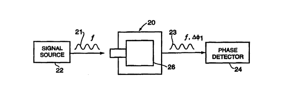
In more detail, FIG. lA shows the resonator 20
before the material being detected is bound to its
surface 26. The resonator 20 is electrically coupled to
a signal source 22, which provides an input electrical
signal 21 having a frequency f within the resonance band
of the resonator. The input electrical signal is
coupled to the resonator 20 and transmitted through the
resonator to provide an output electrical signal 23.
The output electrical signal 23 is at the same frequency
as the input signal 21, but differs in phase from the
input signal by a phase shift ~~1, which depends on the
piezoelectric properties and physical dimensions of the
resonator. The output signal 23 is coupled to a phase
detector 24 which provides a phase signal related to the
insertion phase shift.
FIG. 1B shows the sensing resonator 20 with the
material being detected bound on its surface 26. The
same input signal is coupled to the resonator 20.
Because the resonant characteristics of the resonator
are altered by the binding of the material as a
perturbation, the insertion phase shift of the output
signal 25 is changed to ~~2. The change in insertion
phase shift caused by the binding of the material is
detected by the phase detector.24. The measured phase
shift change is related to the amount of the material
bound on the surface of the resonator.
This phase detection approach of the invention can
be advantageously used with piezoelectric resonators of
different resonant frequencies and configurations. For
example, the sensing resonators may be conventional
quartz resonators or the more recently developed thin-
film resonators. Nevertheless, thin-film resonators are
generally preferred because of their high resonance
SUBSTITUTE SHEET (RULE 26)
CA 02295225 1999-12-23
WO 99/00855 PCT/US98/13535
9
frequencies and the accompanying higher sensitivities.
Depending on the applications, a thin-film resonator
used as the sensing element may be formed to support
either longitudinal or shear bulk-acoustic wave resonant
modes. Longitudinal-mode TFR sensors can be effectively
used in a vacuum or gaseous environment. On the other
hand, shear-mode TFR sensors are more suitable for use
in a liquid sample. This is because a longitudinal-mode
resonance is severely damped by the presence of liquid
at the surface, while a shear mode resonance is only
partially damped.
FIG. 2 shows a simple sensor system embodying the
invention that has a one-port resonator 27 as the
sensing element. A one-port resonator has one electrode
that is used for both signal input and output. The
other electrode of the one-port resonator is typically
grounded. As illustrated in FIG. 2, a signal source 28
provides an input signal which has a frequency within
the resonant bandwidth of the sensing resonator 27. The
input signal is coupled to a power divider 30, which
splits the input signal into two portions. One portion
of the input signal is sent through a coupler 32 to the
input/output electrode 29 of the resonator 27.
The input signal is transmitted across the
resonator 27 and reflected back to the electrode 29.
The output signal, i.e., the reflected signal which has
an insertion phase shift with respect to the input
signal, is then conducted to the coupler 32. The
coupler 32 is a directional device that is capable of
separating the output signal from the input signal. The
output signal is directed by the coupler 32 to a phase
detector 36 as a sensor signal 35. The second portion
of the input signal is also sent from the power divider
30 to the phase detector 36 as a reference signal 37.
The phase detector 36 processes the sensor signal and
the reference signal to provide a phase signal
indicative of a phase difference between the sensor and
SUBSTITUTE SHEET {RULE 26)
CA 02295225 1999-12-23
WO 99/00855 PCT/US98/13535
reference signals.
In a sensing operation, the sensing resonator is
exposed to the material being detected, and the
insertion phase shift changes as a result of the binding
5 of the material on the surface of the resonator 27.
This change is reflected in the phase signal generated
by the phase detector 36.
One of the important advantages of the phase
detection approach of the invention is that the input
10 signal is maintained at a pre-selected constant
frequency during measurement. A stable signal source
with an adjustable signal frequency is relatively simple
and inexpensive to construct, in contrast to the rather
complicated and expensive temperature-compensated high-
frequency oscillator circuitry required by the
conventional approach of tracking the changing
oscillation frequency of the resonator. As an example,
the signal source 28 may be a frequency synthesizer.
Frequency synthesizers are relatively inexpensive and
readily available.
The phase detector 36 in the illustrated embodiment
includes a double-balanced mixer 44 ( or a mathematical
multiplier) which receives the sensor and reference
signals. The sensor signal and the reference signal can
be expressed respectively as Asencos (fit) and Arefcos (~t-
where o~ is the phase difference between the sensor
signal and the reference signal. The mixer 44
multiplies the sensor signal and the reference signal to
produce a signal
Adet (t) - h (ASenAref) COS (fit) COS (fit-~~)
- L (AsenAref) (1/2) (COS (~~) + COs (2~t-0~) },
where L (ASenAref) is a generic loss function. During a
sensing operation, the output power of the signal source
28 is kept constant. The loss function L (ASenAref) is
therefore a constant. The term L (ASenAref) (1/2) cos (~~)
SUBSTITUTE SHEET (RULE 26)
CA 02295225 1999-12-23
WO 99/00855 PCT/IJS98/13535
11
varies with the phase difference, 0~, but does not vary
with time, i.e., it is a DC term. The output of the
mixer 44 is passed through a low-pass filter 46 which
eliminates the time dependent term in Adet and leaves
only the DC term as the output of the phase detector 36.
In this way, the phase detector provides a DC voltage
signal indicative of a phase difference between the
sensor signal and the reference signal. The measured
phase shift change can be used to derive the total
amount of the material bound on the surface of the
sensing resonator. Alternatively, the DC voltage signal
can be monitored as a function of time to determine the
rate at which the insertion phase shift changes. This
rate of change relates to the rate at which the material
being detected binds to the surface of the sensing
resonator 27. If the resonator is used in an aqueous
environment, the rate of change provides an indication
of the concentration or density of the material being
detected in the liquid.
In many applications, the exposure of a sensing
resonator to the material being detected involves
subjecting the resonator to different environmental
conditions which can also alter the resonant
characteristics of the resonator. For instance, when
used as a thickness monitor in an epitaxial deposition
operation, the resonator is often subjected to heat
which could shift the resonance frequency. As another
example, if the resonator is submerged in a liquid to
detect the existence of certain molecules in the liquid,
the contact of the surface with the liquid also
introduces certain viscosity loading effects that are
separate from the effects caused by the binding of the
molecules on the surface. Such environmental effects
can mask the phase change caused by the material being
detected and generate erroneous results.
In accordance with an aspect of the invention, such
environmental effects are effectively distinguished from
SUBSTITUTE SHEET (RULE 26)
CA 02295225 1999-12-23
WO 99/00855 PCT/US98/13535
12
the material binding effects by the use of a reference
resonator. The reference resonator preferably has
resonant characteristics sufficiently close to those of
the sensing resonator so that the phase shifts of the
two resonators caused by the environmental effects are
very similar in magnitude. During the sensing
operation, the sensing and reference resonators are
subject to substantially identical environmental
conditions. Nevertheless, the material to be detected
is prevented from binding on the surface of the
reference resonator. This can be achieved by blocking
the surface of the reference resonator from the material
being detected, or by coating only the sensing resonator
to provide the needed binding sites for the material.
Due to the similar resonant characteristics of the
sensing and reference resonators, the environmental
conditions are expected to cause substantially the same
insertion phase shift change in the two resonators.
Since the material being detected does not bind on the
reference resonator, the phase shift change of the
reference resonator reflects mainly the environmental
effects. The phase shift change of the reference
resonator is subtracted from the total phase shift
change of the sensing resonator to provide a difference
signal which reflects mainly the material binding
effects.
FIG. 3 shows a sensing system which has a one-port
sensing resonator 50 and a one-port reference resonator
52. The signal source, power divider, and phase
detector used in this system are identical to those in
the system of FIG. 2 and are therefore identically
numbered. The sensing resonator 50 and the reference
resonator 52 preferably have very similar resonant
characteristics and substantially overlapping resonant
bands. The signal source 28 provides an input signal of
a frequency which is within the overlapping portion of
the resonant bands of the resonators and preferably is
SUBSTITUTE SHEET (RULE 26j
CA 02295225 1999-12-23
WO 99/00855 PCTNS98/13535
13
set equal to the average of the resonance frequencies of
the two resonators. The input electrical signal
provided by the signal source 28 is split by a power
divider 30 and the split signals are coupled through
couplers 56, 58 to the respective sensing and reference
resonators 50, 52. The output signals of the resonators
are directed to the phase detector 36 by the respective
couplers 56, 58 as sensor and reference signals. The
phase detector 36 processes the sensor and reference
signals to produce a phase signal indicative of a phase
difference between the two signals. As described above,
this phase difference is expected to be caused mainly by
the binding of the material being detected on the
surface of the sensing resonator 50.
The phase detection according to the invention can
also be advantageously implemented with two-port
resonators. A two-port resonator has one electrode for
receiving an input signal, and a second electrode for
providing an output signal. FIG. 4 shows a sensing
system which has a two-port sensing resonator 60 and a
two-port reference resonator 62. The sensing and
reference resonators preferably have very similar
resonant characteristics, and the resonant bands of the
two resonators substantially overlap with each other. A
signal source 28 provides an input electrical signal
which has a frequency within the overlapping portion of
the resonant band of the two resonators. The input
signal is split by a power divider 30, and the split
signals are coupled to the respective input electrodes
64, 66 of the sensing and reference resonators 60, 62.
The input signals are transmitted through the resonators
to form output electrical signals at the respective
output electrodes 68, 70 of the sensing and reference
resonators. The output signals of the two resonators
are coupled to the phase detector 36, which produces a
phase signal indicative of a phase difference between
the two output signals. Quantitative information of the
SUBSTITUTE SHEET (RULE 26)
CA 02295225 1999-12-23
WO 99/00855 PCT/US98/13535
14
~ material bound on the surface of the sensing resonator
can then be derived from the phase signal.
In a particularly advantageous embodiment of the
invention, the two-port reference/sensing resonator
combination described above is implemented as a
monolithically fabricated three-port device which
comprises basically two two-port thin-film resonators
with their input electrodes connected to a common input.
As illustrated in FIGS. 5A and 5B, the two resonators
72, 74 are supported on a thin Si02 layer 76 which is
thermally grown on a silicon substrate 78. The Si02
layer 76 has a thickness of about 1000 A. The Si
substrate 78 has thickness of about 345 lam, a width of 4
mm and a length of 12 mm. The portions of the Si
substrate under the resonators are etched away to allow
the resonators to undergo resonant movement. The bottom
of the Si substrate 78 has a layer of silver paint 80
applied thereto which serves as a grounding plane.
In the illustrated embodiment, the resonator 72 has
an epitaxially deposited A1N layer 82 grown to a
thickness of about 2.35 um to provide a shear mode
resonance frequency of 900 MHz. Alternatively, the
piezoelectric layer may be formed of ZnO. The A1N layer
82 is in the shape of a square of side width of 500 um.
A rectangular input electrode 86 and a rectangular
output electrode 88 are formed on opposite sides of the
piezoelectric layer 82. Each of the electrodes 86, 88
is a 0.5 um thick A1 layer. The width of the electrodes
is about 200 um. The overlapping portion of the two
electrodes 86, 88 defines a square active area of the
resonator 72, which is about 200 um by 200 um. The size
of the active area of the resonator is selected to keep
the static capacitance of the resonator sufficiently
small to avoid distortion of the phase response of the
resonator around resonance. With the chosen size and
thickness of the active area of the resonator, the
static capacitance is about 0.64 pF.
SUBSTITUTE SHEET (RULE 26)
CA 02295225 1999-12-23
WO 99/00855 PCT/US98/13535
The other resonator 74 is generally a mirror image
of the resonator 72, with an A1N layer 84 formed between
an input electrode 90 and an output electrode 92. Due
to the symmetry of the two resonators, either resonator
5 can be prepared, such as by applying a proper coating,
for use as the sensing resonator. The other resonator
is then used as the reference resonator.
The input electrical signal is coupled to the two
resonators via a transmission line 96 formed on the
10 substrate. The transmission line 96 is a deposited A1
strip which has a width of 277 um and a thickness of 0.5
um. The dimensions of the transmission line are chosen
to provide a 50 S2 impedance on the Si substrate.
Similar transmission lines 97, 98 are connected to the
15 output electrodes 88, 92 of the two resonators 72, 74,
respectively, for coupling the respective output signals
to a phase detector.
The transmission line 96 conducts the input
electrical signal to a power divider 91 which splits the
input electrical signal into two portions. The split
signals are conducted to the respective input electrodes
86, 90 of the two resonators by a deposited A1 strip 94
which has the same width as the input electrodes. In
the illustrated embodiment, the power divider 91 is in
the form of a T-junction of the transmission line 96 and
the connecting strip 94. This T-junction power divider
is simple in structure and easy to fabricate.
Nevertheless, other types of power dividers may also be
used. For example, the T-junction may be replaced by a
Wilkinson power divider which is only slightly more
complicated in design but provides better isolation
between the two resonators.
It is an important advantage of the embodiment that
the two resonators are disposed close to each other on
the same substrate. The proximity ensures that the two
resonators are subjected to substantially identical
environmental conditions during a material sensing
SUBSTITUTE SHEET (RULE 2fij
CA 02295225 1999-12-23
WO 99/00855 PCT/US98/13535
16
operation. On the other hand, sufficient distance
should be provided to reduce cross talk between the two
resonators. In the illustrated embodiment, the centers
of the two resonators are separated by about 2000 um.
Another important advantage of forming the sensing
and reference sensors in close proximity on the same
substrate is that the two resonators are likely to have
closely matched resonant frequencies and phase
responses. The matched phase responses allow accurate
phase shift measurements and effective cancellation of
environmental effects.
It will be appreciated by those skilled in the art
that the general structure of the monolithic
sensing/reference resonator combination described above
can be used to fabricate sensing devices with more than
two resonators on a given substrate. For instance, two
or more three-port TFR devices each having a sensing
resonator and a reference resonator can be
monolithically fabricated on one substrate. During a
sensing operation, the output of the sensing resonator
in each three-port device can be referenced to the
output of the reference resonator in the same device.
Alternatively, the sensor can be formed as a multiple-
port device with one reference resonator and two or more
sensing resonators, with the input electrodes of the
resonators connected to a common signal input. During a
sensing operation, the output of each of the sensing
resonators is referenced to the output of the reference
resonator.
It will also be appreciated that other types of TFR
structures may be used to fabricate multiple-resonator
sensors for use with the phase detection technique of
the invention. For instance, a resonator network
illustrated in FIG. 7A of U.S. Patent 5,231,327 to
Ketcham includes two resonators which share a common
input electrode. One of the resonators may be used as
the reference resonator, and the other the sensing
SUBSTITUTE SHEET (RULE 26)
CA 02295225 1999-12-23
WO 99/00855 PCT/IJS98/13535
17
resonator. The '327 patent is hereby incorporated by
reference.
To further illustrate the operating principles of
the invention, FIGS. 6A and 6B show measured results
taken with a longitudinal-mode three-port TFR sensing
device which has a sensing resonator and a reference
resonator arranged in the general structure shown in
FIGS. 5A and 5B. The sensor was used to detect Listeria
bacteria in an aqueous sample. For that purpose, the
surface of the sensing resonator was coated with the
antibody for the Listeria bacteria. The antibody
molecules provided strong binding sites for the
bacteria. The surface of the reference sensor was
coated with a different antibody which was not expected
to have significant binding with the Listeria bacteria
in the liquid sample.
FIG. 6A shows the phase curves 102, 104 region for
the sensing and reference resonators, respectively,
taken before the sensing operation. The resonance
frequency of the sensing resonator was 840.1 MHz, as
indicated by the marker 106, and the resonance frequency
of the reference resonator was 834.5 MHz, as indicated
by the marker 108. It can be seen that the phase bands
of the two resonators have significant overlap.
The sensor was used in the phase detection system
of FIG. 4. The frequency of the input electric signal
for the two resonators was set close to 837.25 MHz
(indicated by the marker 110), which was about the
medium of the resonant frequencies of the two
resonators. At that frequency, the insertion phase
difference between the sensing and reference resonators
was about 41 degrees.
The three-port sensor was then submerged in the
liquid sample containing the material to be detected,
namely Listeria bacteria. The sensor was left in the
liquid for 5 minutes to allow the bacteria to bind to
the antibody-coated surface of the sensing resonator.
SUBSTITUTE SHEET (RULE 26)
CA 02295225 1999-12-23
WO 99/00855 PCT/US98/I3535
18
Subsequently the sensor was removed from the solution,
rinsed to remove unbound Listeria bacteria and then air
dried. FIG. 6B shows the measured phase curves 112, 114
of the two resonators after this binding procedure. It
will be appreciated that the phase curves of the
resonators are provided in FIGS. 6A and 6B only for the
purpose of illustrating the operating principles of the
invention. If the sensing system of FIG. 4 is used, it
will not be necessary to scan over the entire resonance
region. Instead, the input signal will be set at a
constant frequency, such as 837.25 MHz, and the phase
difference between the resonators at that frequency will
be detected and indicated by the phase signal generated
by the phase detector.
As can be seen in FIGS. 6A and 6B, the phase
difference between the sensing resonator and the
reference resonator was altered by the binding process.
At the input signal frequency of 837.25 MHz indicated by
the marker 110, the phase difference between the two
resonators was reduced to about 30 degrees. Thus, the
binding of the material being detected on the surface of
the sensing resonator changed the insertion phase
difference by about 11 degrees at the selected input
frequency of 837.25 MHz.
It should now become appreciated that what is
provided is a method and system for sensing a given
material with a piezoelectric sensor that transmits a
constant-frequency input signal through the sensing
resonator and measures changes in the insertion phase
shift, which are caused by the binding of the material
being detected on the sensing resonator. The insertion
phase shift change provides quantitative information of
the material being detected. By virtue of the constant
signal frequency in the phase detection, simple and
inexpensive input signal sources can be used. The phase
detection approach also allows effective cancellation of
environmental effects on the measurement by the use of a
SUBSTITUTE SHEET (RULE 26)
CA 02295225 1999-12-23
WO 99/00855 PCT/US98/13535
19
reference resonator driven by the same input electrical
signal. In the preferred embodiment, the sensing and
reference resonators are monolithically formed as a
thin-film multiple-port sensing device. The monolithic
construction ensures close matching of the resonant
characteristics of the sensing and reference resonators,
thereby allowing accurate measurement and effective
cancellation of environmental effects.
SUBSTITUTE SHEET (RULE 26)