Language selection

Search

Patent 2295248 Summary

Third-party information liability

Some of the information on this Web page has been provided by external sources. The Government of Canada is not responsible for the accuracy, reliability or currency of the information supplied by external sources. Users wishing to rely upon this information should consult directly with the source of the information. Content provided by external sources is not subject to official languages, privacy and accessibility requirements.

Claims and Abstract availability

Any discrepancies in the text and image of the Claims and Abstract are due to differing posting times. Text of the Claims and Abstract are posted:

  • At the time the application is open to public inspection;
  • At the time of issue of the patent (grant).
(12) Patent: (11) CA 2295248
(54) English Title: POWER DEVICES IN WIDE BANDGAP SEMICONDUCTOR
(54) French Title: DISPOSITIFS DE PUISSANCE DANS UN SEMI-CONDUCTEUR A LARGE BANDE
Status: Deemed expired
Bibliographic Data
(51) International Patent Classification (IPC):
  • H01L 29/78 (2006.01)
  • H01L 21/76 (2006.01)
  • H01L 29/10 (2006.01)
  • H01L 29/24 (2006.01)
  • H01L 29/739 (2006.01)
(72) Inventors :
  • COOPER, JAMES ALBERT JR. (United States of America)
  • MELLOCH, MICHAEL R. (United States of America)
  • SHENOY, JAYARAMA (United States of America)
  • SPITZ, JAN (United States of America)
(73) Owners :
  • COOPER, JAMES ALBERT JR. (United States of America)
  • MELLOCH, MICHAEL R. (United States of America)
  • SHENOY, JAYARAMA (United States of America)
  • SPITZ, JAN (United States of America)
(71) Applicants :
  • COOPER, JAMES ALBERT JR. (United States of America)
  • MELLOCH, MICHAEL R. (United States of America)
  • SHENOY, JAYARAMA (United States of America)
  • SPITZ, JAN (United States of America)
(74) Agent: SIM & MCBURNEY
(74) Associate agent:
(45) Issued: 2006-08-29
(86) PCT Filing Date: 1998-06-23
(87) Open to Public Inspection: 1998-12-30
Examination requested: 2003-05-08
Availability of licence: N/A
(25) Language of filing: English

Patent Cooperation Treaty (PCT): Yes
(86) PCT Filing Number: PCT/US1998/013003
(87) International Publication Number: WO1998/059374
(85) National Entry: 1999-12-16

(30) Application Priority Data:
Application No. Country/Territory Date
60/050,562 United States of America 1997-06-23

Abstracts

English Abstract


An insulated gate power semiconductor switching device (11) such as a lateral
DMOSFET or a lateral IGBT disposed on a
semi-insulating substrate (12). In particular, the substrate may consist of
semi-insulating silicon carbide, eg. vanadium-doped SiC. Accordingly,
high voltage lateral field-effect can be manufactured using readily available
silicon carbide wafers having epilayers of about 10-15
micrometers.


French Abstract

L'invention concerne des dispositifs préférés qui comprennent un dispositif à semi-conducteur tel qu'un dispositif de commutation de très haute puissance fabriqué sur un substrat isolé par jonction ou semi-isolant (par exemple, du carbure de silicium).

Claims

Note: Claims are shown in the official language in which they were submitted.


-5-

CLAIMS:

1. A power switching device, comprising:
a substrate;
a drift region layer adjacent to said substrate;
a source region, a drain region, and a channel region
provided within the drift region layer, wherein said
channel region encircles the lower boundary of said source
region;
an insulating layer over said channel region: and
a gate adjacent to said insulating layer;
wherein said substrate is a semi-insulating substrate.

2. The device of Claim 1, which is a transistor.

3. The device of. Claim 2, which is an insulated gate
field effect transistor.

4. The device or Claim 2, which is an insulated gate
bipolar transistor.

5. The device of Claim 1, wherein the source and drain
are N+, the channel is P, and the drift region is N-.

6. The device of Claim 1, wherein the semiinsulating
substrate is silicon carbide.

7. The device of Claim 6, wherein the semiinsulating
substrate is coped with vanadium.

8. A power switching device, comprising:
a substrate;
a drift region layer adjacent to said substrate;
a source region, a drain region, and a channel region
provided within the drift region layer wherein said channel
region encircles the lower boundary of Said source region;
an insulating layer over said channel region; and
a gate adjacent to said insulating layer;
wherein said substrate is a junction-isolated
substrate.

Description

Note: Descriptions are shown in the official language in which they were submitted.


CA 02295248 2003-05-08
POWER DEVICES IN WII;aE, BANL~C~F~E~' SE;M:LCONhUC".':~'OR.
Backcxroun;i o~ the :Lrrvent ion
The present invent:ic~r~. relates gerre:rally to
semiconductor devices anc;~ in part.:it~:u:.~~-rx- too high
voltage/high power devic~e:~ ft~b:ri.c~;~t_ec orr semi-insulating
substrates such as semi--~r~,~ui.at:i.r~:.y si l._i~~or~ carbide. For
additional backgr_~ound infc>rrnat:i_orr, irrc~Luding information
pertaining to basic semac:~ond;actor ~F~v ~.c~~ elerr~ents
incorporated irn ~aev:iLes c-.~f tJne px-~.~~er~rt; ira.vention,
reference can be made, for e~:arn~>1.G3, t:.,.:> ~J. S . Fatent~s Nos .
5, 448, 081; 5, 378, 912 arrct ~j , 9.~;:~, ~:> ~3 .
Patent A:bstx~acts of Japan Pu.bLi.c~atic:~n No. 08213606
(published Augusts 20, 19~>6j ;:~esr.~.r:i~~es a lateral high
breakdown strength NIOSFEa' having au n-P- substrate . German
publication No. X328804 A1_ dc~sc:ri.b~:~s ~::~ process for
producing hig:h--:resistar~.cc:a S:iC fx°on~ lo~a4-:resistance ~SiC
starting material. . United States ~:~at:c:>nt~ Nc. 5, 61.1, 955
describes a high resistivi.ty sil.ic~:>n ~::°a:rbi.de substrate
for use in sem:iconduc:tox~ devices . Unit.wd States Patent
No. 5, 378, 912 describes a lateral w:,c~m:i_conductor-on-
insulator ( SOI j c~evi c:e .
Sunuma~:~,~ c>:E t~~r~~ I:rrvaant:ion
One ob j ect of an aspE:ct of t hr~ pu-esent invent ion is
to provide devices which allow blo~:~kirrg of very high
voltages without trne~ need foci ~.~ ver y P~hick drift region
which must be gr~~~wn by epitax;y.
Another object oaf are. aspect oI~ the present invention
is to provide a :hater al power clev:ir~e _structure, such as a

~
CA 02295248 2006-02-17
-2-
very high voltage (greater than 1000 v up to and greater
than 10000 v) power switching device, fabricated on a
junction-isolated or semi-insulating substrate in a wide
bandgap semiconductor having a breakdown field
substantially greater than silicon.
Another object of an aspect of the present invention
is to provide such lateral power devices in the form of a
lateral metal oxide semiconductor field effect transistor
(MOSFET) or lateral insulated gate bipolar transistor
(IGBT) on silicon carbide.
Accordingly, one preferred embodiment of the
invention provides a lateral power device structure
fabricated in an epilayer (epitaxially-grown layer) on a
semi-insulating substrate, especially a semi-insulating
silicon carbide substrate. Such a semi-insulating
substrate can be achieved, for instance, by doping, e.g.,
with vanadium or similar dopant materials. The preferred
devices include a semi-insulating silicon carbide
substrate, and an epitaxially grown drift region (e. g.,
N-) adjacent the semi-insulating substrate (e. g., doped
at a level of about 2-5 x 1015 cm-3). A lateral
semiconductor device, e.g., an insulated gate field
effect transistor (or MOSFET) or IGBT is provided in the
epilayer. Such devices include generally source and
drain regions (e. g., both N+), an insulating layer (e. g.,
Si02), and a gate, e.g., formed of polysilicon. Other
conventional semiconductor device features can also be
included, as those skilled in the art will appreciate.
According to one aspect of the present invention,
there is provided a power switching device comprising:
a substrate;
a drift region layer adjacent to said substrate;
a source region, a drain region, and a channel
region provided within the drift region layer, wherein

~
CA 02295248 2006-02-17
-2a-
said channel region encircles the lower boundary of
said source region;
an insulating layer over said channel region; and
a gate adjacent to said insulating layer;
wherein said substrate is a semi-insulating
substrate.
According to another aspect of the present
invention, there is provided a power switching device
comprising:
a substrate;
a drift region layer adjacent to said substrate;
a source region, a drain region, and a channel
region provided within the drift region layer wherein
said channel region encircles the lower boundary of said
source region;
an insulating layer over said channel region; and
a gate adjacent to said insulating layer;
wherein said substrate is a junction-isolated
substrate.
Additional objects, embodiments, and features of the
invention will be apparent from the following
descr=_;- __ __a ~~._ ~,~.,..: ~~.. ..~~..~.a...~ ~,..~...~..


CA 02295248 1999-12-16
-3-
Brief Description of the Drawings
Figure 1 shows a preferred lateral power device of
the present invention.
Figure 2 shows depletion edges for several
blocking voltages in an illustrative lateral power
device of the present invention.
escription of the Preferred Embodiment
For the purposes of promoting an understanding of
the principles of the invention, reference will now be
made to certain preferred embodiments thereof and
specific language will be used to describe the same.
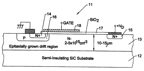
Figure 1 shows a preferred lateral power device 11
of the present invention. Device 11 includes a semi-
insulating layer 12, e.g., a semi-insulating silicon
carbide substrate. Adjacent to layer 12 is an
epitaxially-grown layer providing drift region 13
(e. g., N-). Drift region 13 may be doped, for example,
at a l eve 1 o f about 2 - 5 x 1 O 15 at / cm-3 , and may have a
thickness of up to about 15 ~,m, e.g., about 10 to about
15 Vim. Provided within layer 13 are source and drain
regions 14 and 15 (which of opposite character to drift
region 13, e.g., in the illustrated device N+; or, to
provide an IGBT, drain region 15 can be P+), and a
channel region 16. Also provided in device 11 is an
insulating layer 17 (e. g., SiOz) covering the channel
region 16, and a gate 18 adjacent the insulating layer
17, for example formed with polysilicon (doped).
Additional features may also be included in the device,
for example conductive materials such as metals) to
provide leads at the source and drain.
In an illustrative device such as that illustrated
in Figure 1, in the off, or blocking condition, the PN-


CA 02295248 1999-12-16
- -4-
junction will extend a depletion region about 56 ~,m
into the N- region before avalanche breakdown occurs
(assuming a doping of 2 x 1015 cm-3). This would
correspond to a drain voltage of V=Emax/2 Vd = 5600v.
Lateral structures in accordance with the preferred
devices of the invention are particularly advantageous,
since silicon carbide wafers with epilayers of about
10-15 um are currently readily available commercially.
In the present invention, the semi-insulating substrate
ensures that the substrate does not act as an
L equipotential boundary under the depleted drift region,
which would confine the extent of the electric field to
the regions under the base (P) region and under the
drain (N+) region. Shown in Figure 2 are approximate
depletion edges for several blocking voltages in an
illustrative device of the present invention.

Representative Drawing
A single figure which represents the drawing illustrating the invention.
Administrative Status

For a clearer understanding of the status of the application/patent presented on this page, the site Disclaimer , as well as the definitions for Patent , Administrative Status , Maintenance Fee  and Payment History  should be consulted.

Administrative Status

Title Date
Forecasted Issue Date 2006-08-29
(86) PCT Filing Date 1998-06-23
(87) PCT Publication Date 1998-12-30
(85) National Entry 1999-12-16
Examination Requested 2003-05-08
(45) Issued 2006-08-29
Deemed Expired 2014-06-25

Abandonment History

There is no abandonment history.

Payment History

Fee Type Anniversary Year Due Date Amount Paid Paid Date
Application Fee $300.00 1999-12-16
Maintenance Fee - Application - New Act 2 2000-06-23 $100.00 1999-12-16
Maintenance Fee - Application - New Act 3 2001-06-25 $100.00 2001-05-18
Maintenance Fee - Application - New Act 4 2002-06-24 $100.00 2002-05-16
Request for Examination $400.00 2003-05-08
Maintenance Fee - Application - New Act 5 2003-06-23 $150.00 2003-05-28
Maintenance Fee - Application - New Act 6 2004-06-23 $200.00 2004-06-07
Maintenance Fee - Application - New Act 7 2005-06-23 $200.00 2005-05-31
Expired 2019 - Filing an Amendment after allowance $400.00 2006-02-17
Final Fee $300.00 2006-04-26
Maintenance Fee - Application - New Act 8 2006-06-23 $200.00 2006-06-13
Maintenance Fee - Patent - New Act 9 2007-06-25 $200.00 2007-05-07
Maintenance Fee - Patent - New Act 10 2008-06-23 $250.00 2008-05-12
Maintenance Fee - Patent - New Act 11 2009-06-23 $250.00 2009-05-14
Maintenance Fee - Patent - New Act 12 2010-06-23 $250.00 2010-05-11
Maintenance Fee - Patent - New Act 13 2011-06-23 $250.00 2011-05-11
Maintenance Fee - Patent - New Act 14 2012-06-25 $250.00 2012-05-10
Owners on Record

Note: Records showing the ownership history in alphabetical order.

Current Owners on Record
COOPER, JAMES ALBERT JR.
MELLOCH, MICHAEL R.
SHENOY, JAYARAMA
SPITZ, JAN
Past Owners on Record
None
Past Owners that do not appear in the "Owners on Record" listing will appear in other documentation within the application.
Documents

To view selected files, please enter reCAPTCHA code :


To view images, click a link in the Document Description column. To download the documents, select one or more checkboxes in the first column and then click the "Download Selected in PDF format (Zip Archive)" or the "Download Selected as Single PDF" button.

List of published and non-published patent-specific documents on the CPD .

If you have any difficulty accessing content, you can call the Client Service Centre at 1-866-997-1936 or send them an e-mail at CIPO Client Service Centre.


Document
Description 
Date
(yyyy-mm-dd) 
Number of pages   Size of Image (KB) 
Representative Drawing 2000-02-25 1 5
Claims 2003-05-08 2 51
Description 2003-05-08 5 221
Cover Page 2000-02-25 1 37
Abstract 1999-12-16 1 57
Description 1999-12-16 4 159
Claims 1999-12-16 2 40
Drawings 1999-12-16 1 19
Claims 2005-04-04 1 34
Representative Drawing 2005-11-17 1 9
Description 2006-02-17 5 191
Cover Page 2006-07-31 1 41
Assignment 1999-12-16 3 116
PCT 1999-12-16 16 560
Prosecution-Amendment 2003-05-08 7 266
Prosecution-Amendment 2003-05-08 1 38
Prosecution-Amendment 2003-09-09 1 26
Correspondence 2006-04-26 1 52
Prosecution-Amendment 2004-10-05 2 63
Prosecution-Amendment 2005-04-04 6 313
Prosecution-Amendment 2006-02-17 4 131
Prosecution-Amendment 2006-03-21 1 17