Note: Descriptions are shown in the official language in which they were submitted.
CA 02295382 2000-O1-14
- 1 -
HACRGROUND OF THE INVENTION
1. Field of the Invention
The present invention relates to a switching power supply
unit, and more particularly to a switching power supply unit
of a self-excitation-type ringing choke converter (hereinafter
abbreviated as RCC) system.
2. Descri~~tion of the Related Art
In general, electronic equipment, such as electronic
calculators or communication devices, needs a stable DC
voltage. Thus, in order to supply a stable DC voltage to such
electronic equipment from a commercial AC power supply,
switching power supply units of the RCC system, in which
relatively easy construction is possible to obtain high
efficiency, have been widely used. A structure of such a
switching power supply unit will be illustrated referring to
Fig. 6.
In this figure, reference numeral 1 indicates a switching
power supply unit, which has an input circuit 2, a main
operation circuit 3, a voltage detection circuit 4, a control
circuit 5, an output terminal OUT, and a ground terminal GND.
Among these components, the input circuit 2 has a
rectifying diode bridge DB, a fuse F, and a filter circuit LF.
Both the fuse F and the filter circuit are disposed between an
AC power supply and an input end of the rectifying diode
bridge DB.
In addition, the main operation circuit 3 has a smoothing
capacitor C1 disposed between the output ends a and b of the
diode bridge DB of the input circuit 2, a transformer T having
a primary winding N1, a secondary winding N2 having the
polarity opposite to that of the primary winding N1 and a
feedback winding NB with the same polarity as that of the
primary winding N1, an FET Q1 as a main switching element
CA 02295382 2000-O1-14
- 2 -
connected in series to an end of the primary winding N1 of the
transformer T, a starting resistor R1 connected between the
other end of the primary winding N1 and the gate as the
control terminal of the FET Q1, a resistor RS connected
between the gate and source of the FET Q1, a rectifying diode
D1 connected in series to an end of the secondary winding N2
of the transformer T, and a smoothing capacitor C4 connected
between an end of the secondary winding N2 and the output
terminal.
The voltage detection circuit 4, which is disposed on the
output side of the main operation circuit 3, includes a
resistor R5, a light-emitting diode PD on the light-emitting
side of a photo coupler PC, a shunt regulator Sr, and
resistors R6 and R7. Among these components, the resistor R5,
the anode and cathode of the light-emitting diode PD, and the
cathode of the shunt regulator Sr are mutually connected in
series and are disposed in parallel to the capacitor C4 of the
main operation circuit 3. In addition, the resistors R6 and R7
are also mutually connected in series and are also disposed in
parallel to the capacitor C4. The node of the resistors R6 and
R7 is connected to a reference of the shunt regulator Sr.
Furthermore, the control circuit 5 includes a resistor R9
and a capacitor C3 connected in series between one end of the
feedback winding NB and the gate of the FET Q1, a transistor
Q2 connected between the gate and source of the FET Q1, a
resistor R2 connected between one end of the feedback winding
NB and the base of the transistor Q2, a resistor R3 and a
capacitor C2 connected in parallel between the base and
emitter of the transistor Q2, a resistor R4, a diode D2, and a
photo transistor PT on the light-receiving side of the photo
coupler PC, which are mutually connected in series between one
end of the feedback winding NB and the base of the transistor
Q2.
Next, a description will be given of the operation of a
switching power supply unit 1 having such a structure.
CA 02295382 2000-O1-14
- 3 -
First, on startup, a voltage is applied to the gate of
the FET Q1 via the resistor R1 to turn on the FET Q1. When the
FET Q1 is turned on, a power supply voltage is applied to the
primary winding N1 of the transformer T, and then, at the
feedback winding NB is generated a voltage of the same
direction as that of the voltage generated at the primary
winding N1, whereby the FET Q1 is rapidly turned on by a
positive feedback. In this situation, excitation energy is
charged in the primary winding N1.
After that, when the base potential o~ the transistor Q2
reaches a threshold, the transistor Q2 is turned on, whereas
the FET Q1 is turned off. This permits the excitation energy
charged in the primary winding N1 of the transformer T during
the ON time of the FET Q1 to be discharged as electric energy
via the secondary winding N2. The energy is rectified by the
diode D1 and is smoothed by the capacitor C4 to be supplied to
a load.
When the excitation energy charged in the primary winding
N1 of the transformer T is discharged via the secondary
winding N2, a fly-back voltage VNB is generated at the
feedback winding NB. Changes in the fly-back voltage VNB will
be illustrated referring to Fig. 7. In this figure, at a
point-in-time tll, the FET Q1 is turned off and the fly-back
voltage VNB is maintained at an almost fixed value to enter
the so-called OFF time. Then, at a point-in-time t12, the
voltage of the diode D1 becomes zero, and the fly-back voltage
VNB begins to resonate. At a point-in-time t13, when the fly-
back voltage VNB reaches a threshold Vth of the FET Q1, the
FET Q1 is turned on. The dotted line of the fly-back voltage
VNB indicates changes in a case where it is assumed that the
fly-back voltage VNB continues to resonate even after the
turn-on of the FET Q1. In this way, when the FET Q1 is turned
on, a voltage is again applied to the primary winding N1 of
the transformer T, whereby excitation energy is again charged
in the transformer primary winding.
CA 02295382 2000-O1-14
- 4 -
In the switching power supply unit 1, the above-described
oscillating operation is repeated.
In a steady state, the output voltage of the load is
divided by the resistors R6 and R7, and the divided detection
voltage is compared with a reference voltage of the shunt
regulator Sr. After the comparison, the amount of fluctuations
in the output voltage is amplified by the shunt regulator Sr,
and current flowing to the light-emitting diode PD of the
photo coupler PC changes, in which the impedance of the photo
transistor PT changes according to the light-emitting amount
of the light-emitting diode PD. This operation permits the
time for charging / discharging the capacitor C2 to be changed,
so that the output voltage is regulated.
In the conventional switching power supply unit 1,
however, switching losses under light load are large, which
leads to reduced circuit efficiency.
The present invention can solve the aforementioned
problem and provide a switching power supply unit capable of
suppressing increase in switching losses under light load.
To this end, the present invention provides a switching
power supply unit including a DC power supply, a transformer
having a primary winding, a secondary winding and a feedback
winding, and a main switching element connected in series to
be turned on by a voltage generated at the feedback winding,
so that a DC output can be obtained. In this switching power
supply unit, a voltage dropping circuit for dropping the
output voltage is provided, and the output voltage is dropped
by the voltage dropping circuit to reduce a fly-back voltage
generated at the feedback winding during the OFF time of the
main switching, so that the voltage of a control terminal of
the main switching element is maintained at a lower value than
that of a threshold voltage of the main switching element.
In addition, as the voltage dropping circuit, there are
CA 02295382 2000-O1-14
- 5 -
provided a switching element and a resistor connected in
series to the collector thereof to dispose an impedance
adjustment circuit for changing impedance determining the
output voltage.
Furthermore, as the voltage dropping circuit, there is
provided a reference-voltage adjustment circuit for changing a
reference voltage determining the output voltage.
Furthermore, the voltage dropping circuit is driven by a
signal input from the outside.
According to the switching power supply unit having the
above structure, the voltage dropping means permits an output
voltage to be dropped. In this case, since the fly-back
voltage generated at the feedback winding of the transformer
increases or decrease in proportion to the output voltage,
adjusting the dropping level of the output voltage and
reducing the fly-back voltage generated during the OFF time of
the main switching element allows the voltage of the control
terminal of the main switching element to resonate at a lower
value than that of a threshold voltage, in which the turn-on
of the main switching element by the fly-back voltage can be
prevented. This operation delays the turn-on of the main
switching element and allows the OFF time thereof to be
prolonged, in which the oscillation frequency in the switching
power supply unit is reduced. As a result, increase in
switching losses caused by the rising of the oscillation
frequency can be suppressed so that circuit efficiency can be
improved..
In addition, according to the switching power supply unit
in accordance with the present invention, the switching
element forming the impedance adjustment circuit as the
voltage dropping circuit is turned on, in which impedance for
determining the output voltage is changed or the reference
voltage is changed by impedance generated at the resistor
similarly forming the impedance adjustment circuit so as to
change the output voltage.
CA 02295382 2000-O1-14
- 6 -
For the purpose of illustrating the invention, there is
shown in the drawings several forms which are presently
preferred, it being understood, however, that the invention is
not limited to the precise arrangements and instrumentalities
shown.
BRIEF DESCRIPTION OF THE DRAWING~(S1
Fig. 1 is a circuit diagram of a switching power supply
unit according to a first embodiment of the present invention.
Fig. 2 is an illustrative view showing changes in a
voltage generated at a feedback winding of the switching power
supply unit shown in Fig. 1.
Fig. 3 is a circuit diagram showing a modification of the
switching power supply unit shown in Fig. 1.
Fig. 4 is a circuit diagram showing a switching power
supply unit according to a second embodiment of the present
invention.
Fig. 5 is a circuit diagram showing a switching power
supply unit according to a third embodiment of the present
invention.
Fig. 6 is a circuit diagram showing a conventional
switching power supply unit.
Fig. 7 is an illustrative view showing changes in a
voltage generated at a feedback winding of the switching power
supply unit shown in Fig. 7.
DETAILED DESCRIPTION OF EMBODIMENTS OFTHE INVENTION
Hereinafter, the preferred embodiments of the present
invention are explained in detail with reference to the
drawings.
A structure of a switching power supply unit according to
a first embodiment of the present invention will be
illustrated referring to Fig. 1. The switching power supply
unit la shown in the figure is different from the switching
power supply unit 1 shown in Fig. 6 in that an impedance
CA 02295382 2000-O1-14
-
adjustment circuit 6 and a DC-DC converter 7 as a voltage
dropping circuit for dropping an output voltage VO1 are
disposed on the output side of the voltage detection circuit 4.
In this figure, except for the impedance adjustment circuit 6
and the DC-DC converter 7, the same parts as those in Fig. 6
or the equivalent parts thereto are given the same reference
numerals and the explanation thereof is omitted.
In Fig. 1, the impedance adjustment circuit 6 forming the
switching power supply unit la includes a transistor Q3 as a
switching element and resistors R10 and R11. The emitter of
the transistor Q3 is connected to one end of the secondary
winding N2 of a transformer T via a diode D1, whereas the
collector thereof is connected to a shunt regulator Sr of the
voltage detection circuit 4 via the resistor R10. In addition,
the base of the transistor Q3 is connected to a reception
terminal SS via the resistor R11. The reception terminal SS is
connected to an electronic device as a load.
In addition, the DC-DC converter 7 is well known as a
step-up converter, a step-down converter, or a step-up / step-
down converter. The detailed explanation of the structure
thereof is omitted.
In this case, the switching power supply unit la is used
in conjunction with a transmission unit (not shown) disposed
in the electronic device as a load. That is, if the load of
the switching power supply unit la e.g., is a facsimile unit,
in a so-called waiting period (under light load) in which the
power supply of the facsimile unit is turned on, whereas
transmission and reception of data are not being performed, a
signal outputted from the transmission unit (not shown)
disposed in the facsimile unit is applied to the impedance
adjustment circuit 6 via the reception terminal SS of the
switching power supply unit la. This allows the transistor Q3
of the impedance adjustment circuit 6 to be put in a state of
continuity, in which impedance for determining the value of
the output voltage VO1 is generated by the resistor R10 of the
CA 02295382 2000-O1-14
_ $ _
impedance adjustment circuit 6 in addition to the resistors R6
and R7 of the voltage detection circuit 4.
A description will be given about how the value of the
output voltage VO1 varies with such changes in impedance, by
using logical expressions. In the following equations (1) to
(3), reference character Vref denotes the reference voltage of
the shunt regulator Sr, and reference numerals R6, R7, and R10
indicate the resistance values of the resistors R6, R7, and
R10.
The output voltage VO1 obtained when the transistor Q3 of
the impedance adjustment circuit 6 is not in a state of
continuity is indicated by equation (1) below.
VO1 = Vref x {(R6 + R7) / R7} ...(1)
In contrast, the output voltage VO1 obtained when the
transistor Q3 is in a state of continuity is indicated by an
equation (2) below.
VO1=Vref x (1/R7) x {R7+(R6 x R10)/(R6+R10)} ...(2)
Here, an equation (3) below holds.
R6 Z (R6 x R10)/(R6 + R10) ...(3)
In addition, the relationship between the output voltage
VO1 of equation (1) and the output voltage V02 of equation (2)
is indicated by an equation (4) below.
VO1 (the equation(1)) a VO1(the equation(2)) ...(4)
Equation (4) holds only when R10 is infinite.
As described above, when the transistor Q3 conducts and
the impedance for determining the output voltage VO1 changes,
CA 02295382 2000-O1-14
- g -
the output voltage VO1 drops.
In this situation, the absolute value of the fly-back
voltage generated at the feedback winding of the transformer
is a value in proportion to the value obtained by adding a
forward voltage drop of the diode D1 to an output voltage
according to the turn ratio of the feedback winding. In the
switching power supply unit la, advantage is taken that the
absolute value of the fly-back voltage VNB is proportional to
the output voltage VO1 in order to adjust the level of drop of
the output voltage VO1 by the impedance adjustment circuit 6.
In addition, the fly-back voltage VNB generated during the OFF
time of the FET Q1 as a switching element is reduced. With
this arrangement, the switching power supply unit la is set
such that the voltage of the gate as the control terminal of
the FET Q1 resonates at a lower value than a threshold value
at which the FET Q1 turns on.
Fig. 2 shows such changes in the fly-back voltage VNB.
In Fig. 2, at a point-in-time tl, the FET Q1 is turned
off, and after the occurrence of a surge, the fly-back voltage
VNB is maintained at an almost fixed value to enter the so-
called OFF time.
In this situation, the absolute value of the fly-back
voltage VNB during the OFF time is indicated by equation (5)
below. In equation (5), the symbol NB indicates the turn
number of the feedback winding NB of the transformer T, the
symbol N2 indicates the turn number of the primary winding,
and the symbol VF indicates a forward voltage of the
rectifying diode D1 of the main operation circuit 3.
VNB ( - (NB ~ N2) x (VO1 + VF) ...(5)
Furthermore, in proportion to the drop of the output
voltage VO1 due to the operation of the impedance adjustment
circuit 6, the output VO1 included in equation (5) becomes
smaller, whereby the absolute value of the fly-back voltage
CA 02295382 2000-O1-14
- 10 -
VNB is reduced. In other words, the absolute value of the fly-
back voltage VNB of the switching power supply unit in
accordance with the present invention, which is indicated by
the symbol Va in Fig. 2, is smaller than that of the
conventional switching power supply unit, which is indicated
by the symbol Vb in Fig. 7.
Although the fly-back voltage VNB starts to resonate at
the point-in-time t2, since it is maintained at a relatively
low value until the point-in-time t2, amplitude is small and
the value of the gate voltage of the FET Q1 is thereby lower
than the threshold value Vth, with the result that the turn-on
of the FET Q1 by the fly-back voltage VNB is prevented.
After this, at the point-in-time t3, a voltage is applied
to the gate of the FET Q1 by the starting circuit (which is
referred to as the starting resistor R1 in this embodiment) of
the FET Q1 forming the main operation circuit 3 so as to turn
on the FET Q1.
As described above, since the turn-on of the FET Q1 is
delayed and the OFF time thereof is prolonged, the oscillation
frequency is reduced. Therefore, increase in switching losses
due to the rising of the oscillation frequency is suppressed,
which leads to improvement in circuit efficiency.
The dropped output voltage VO1 is stepped up to a desired
value by the DC-DC converter 7 to an output voltage V02, which
is supplied to a load.
Next, a modification of the first embodiment will be
illustrated referring to Fig. 3. In this figure, the same
parts as those in Fig. 1 or the equivalent parts thereto are
given the same reference numerals and the explanation thereof
is omitted.
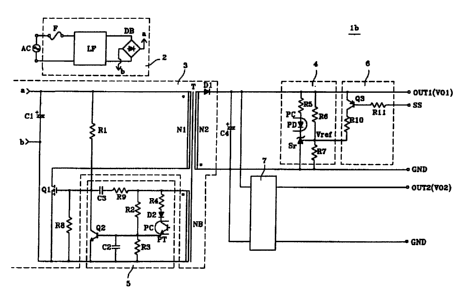
In a switching power supply unit lb shown in Fig. 3, a
DC-DC converter 7 is connected between both ends of a
secondary winding N2 of a transformer T and a voltage
detection circuit 4. An output terminal OUT1 is provided from
an impedance adjustment circuit 6, and an output terminal OUT2
CA 02295382 2000-O1-14
- 11 -
is provided from the DC-DC converter 7. From the output
terminals OUT1 and OUT2, two output voltages VO1 and V02
having mutually different values can be obtained. The
impedance adjustment circuit 6 allows the output voltage VO1
to drop to be supplied to a load. In addition, dropping of the
output voltage VO1 leads to reduction in switching losses and
improvement in circuit efficiency. The DC-DC converter 7
allows the output voltage V02 to be stepped up to a desired
value and to be supplied to the load.
Referring to Fig. 4, a description will be given of a
structure of a switching power supply unit in accordance with
a second embodiment of the present invention. In this figure,
the same parts as those in Fig. 1 and the equivalent parts
thereto are given the same reference numerals and the
explanation thereof is omitted.
In a switching power supply unit lc shown in Fig. 4, a
fly-back voltage VNB generated at a feedback winding NB is
dropped directly by an impedance adjustment circuit 6a. The
switching power supply unit lc includes a control circuit 5a,
the impedance adjustment circuit 6a, and a DC-DC converter 7.
In the control circuit 5a, a transistor Q4 is disposed as
an alternative to the photo coupler PC of the control circuit
5a shown in Fig. 1, and on the base side of the transistor Q4
are disposed resistors R12, R13, R14 and R15, a diode D3, and
a capacitor C5. The operation of the control circuit 5a is the
same as that of a control circuit used in a switching power
supply unit of a conventionally known RCC system and the
explanation thereof is omitted.
In addition, the impedance adjustment circuit 6a, which
is connected between both ends of the feedback winding NB of a
transformer T, has a transistor Q3. The emitter of the
transistor Q3 is connected to an end of the feedback winding
NB of the transformer T, and the collector thereof is
connected to a shunt regulator Srl via a resistor R10. The
shunt regulator Srl is connected to the base of the transistor
CA 02295382 2000-O1-14
- 12 -
Q4 via the resistor R13 of the control circuit Sa. A node of
the resistor R10 and the shunt regulator Srl is connected to
resistors R16 and R17. Moreover, the impedance adjustment
circuit 6a includes a rectifying diode D4 and a smoothing
capacitor C6.
Next, a description will be given of the operation of the
impedance adjustment circuit 6a having the above structure.
In a steady state, the transistor Q3 in the impedance
adjustment circuit 6a does not conduct. Under the situation,
the output voltage VO1 is indicated by equation (6) below. In
the following equations (6) to (9), the symbol Vref indicates
a reference potential of the shunt regulator Sr, and the
symbols R10, R16, and R17 indicate the resistance values of
the resistors R10, R16, and R17. In addition, the symbols N2
and NB respectively indicate voltages generated at the
secondary winding N2 and feedback winding NB of the
transformer T. The symbol VF indicates a forward voltage of
the diode D1.
VO1 = Vref x {(R16 + R17)/R17} x (N2 / NB) + VF ... (6)
Under light load, a signal from an electronic device as a
load is applied to the impedance adjustment circuit 6a via a
reception terminal SS, whereby the transistor Q3 conducts. The
output voltage VO1 obtained in this situation is indicated by
the following equation (7).
V012=Vref x (1/R17)x~Rl7+(R16xR10)/(R16+R17)} ...(7)
In this situation, the following equation (8) holds.
R16 a (R16 x R10)/(R16 + R10) ... (8)
Therefore, the relationship between the output voltage
VO1 of the above equation (6) and the output voltage VO1 of
CA 02295382 2000-O1-14
- 13 -
the above equation (7) is indicated by an inequality (9) below.
VO1 (the equation (6)) > VO1 (the equation (7))... (9)
In this way, when the transistor Q3 conducts and
impedance for determining the output voltage VO1 thereby
changes, the output voltage VO1 drops.
Furthermore, the switching power supply unit lc is set
such that the level of drop of the output voltage VO1 by the
impedance adjustment circuit 6a is adjusted and amplitude is
generated within a range below the threshold of the FET Q1 as
a main switching element. This allows the OFF time of the FET
Q1 to be prolonged so that the oscillation frequency is
reduced, as in the case of the first embodiment. Therefore,
increase in switching losses due to the rising of the
oscillation frequency is suppressed and circuit efficiency can
thereby be improved.
In addition, as the fly-back voltage VNB drops, the
output voltage VO1 having a value proportional to the value of
the fly-back voltage VNB drops. However, the DC-DC converter 7
allows the output voltage VO1 to be stepped up into a desired
value to an output voltage V02, which is supplied to a load.
Although this is not shown in the figure, as a
modification of the switching power supply unit lc shown in
Fig. 4, it is possible to use a switching power supply unit
such as the switching power supply unit lb shown in Fig. 3, in
which the position of the DC-DC converter 7 is changed and the
two output terminals capable of obtaining mutually different
output voltages are provided.
Next, a description will be given of a third embodiment
in accordance with the present invention referring to Fig. 5.
In this figure, the same parts as those in Fig. 1 or the
equivalent parts thereto are given the same reference numerals
and the explanation thereof is omitted.
In a switching power supply unit ld shown in Fig. 5,
CA 02295382 2000-O1-14
- 14 -
instead of the voltage detection circuit 4 and the impedance
adjustment circuit 6, a reference voltage adjustment circuit 8
is disposed as a voltage dropping circuit.
The reference voltage adjustment circuit 8 includes
resistors R5, R6, R7, R10, a light-emitting diode PD of the
light-emitting side of a photo coupler PC, a transistor Q4, a
capacitor C5, a differential amplifier OP, and a voltage
source 9.
The resistor R5, the light-emitting diode PD, and the
transistor Q4 are mutually connected in series and are
disposed in parallel to a capacitor 4 of a main operation
circuit 3. In addition, the resistors R6 and R7 are mutually
connected in series and are similarly disposed in parallel to
the capacitor 4. The node of the resistors R6 and R7 is
connected to an inverting input end of the differential
amplifier OP. A voltage generated at the voltage source 9
changes in response to a signal from an electronic device as a
load. The voltage generated at the voltage source 9 is applied
to the non-inverting input end of the differential amplifier
OP. the output end of the differential amplifier OP is
connected to the base of the transistor Q4.
In this situation, as a reference voltage of the
differential amplifier OP, the voltage generated at the
voltage source 9 is used. The voltage generated at the voltage
source 9 can be referred to as a variable reference voltage
that changes in response to the signal from the electronic
device as a load. The differential amplifier OP and the
transistor Q4 operate as error amplifiers. Both of them
operate to make the potential difference between the positive
(+) and negative (-) terminals zero, with the result that an
output voltage V02 proportionate to the variable reference
voltage can be obtained.
In this case, instead of changing the voltage generated
at the voltage source 9 by the signal from the electronic
device as a load, it is also possible to change the same by a
CA 02295382 2000-O1-14
- 15 -
signal from a transmitter disposed inside the switching power
supply unit ld.
Although this is not shown in the figure, as a
modification of the switching power supply unit ld shown in
Fig. 5, it is possible to use a switching power supply unit
such as the switching power supply unit lb shown in Fig. 3, in
which the position of the DC-DC converter 7 is changed and the
two output terminals capable of obtaining mutually different
output voltages are provided.
The impedance adjustment circuit described in each
embodiment above operates to drop the voltage generated at the
secondary winding NB of the transformer. However, a circuit
having any other structure can be replaced for that, as long
as the circuit operates in the same way.
Furthermore, in each of the embodiments described above,
the switching power supply unit having the two output
terminals has been illustrated as a switching power supply
unit having a plurality of output terminals. However, the
present invention can be applied even in the case of a
switching power supply unit having three or more output
terminals, from each of which an output voltage of a different
value can be obtained.
Furthermore, although each of the embodiments described
above adopts a case in which a transistor is disposed as a
switching element of a voltage dropping circuit, any other
element can be used as an alternative to the transistor, as
long as it operates in the same way as the transistor does.
Furthermore, although each of the embodiments described
above has shown a case in which under light load (in a waiting
time), after the dropping of an output voltage, the DC-DC
converter steps up the voltage, in contrast to this, it is
possible to use a structure in which the DC-DC converter (a
voltage-dropping converter) steps down an output voltage in a
waiting time, whereas the stepped-down output voltage is
outputted without being stepped up / stepped down and stepping
CA 02295382 2000-O1-14
- 16 -
down in a waiting time.
Furthermore, although each of the embodiments described
above has shown a case in which the DC-DC converter steps up
or steps down an output voltage, when the voltage drop in a
waiting time is permitted, it is not necessary to provide a
DC-DC converter.
While preferred embodiments of the invention have been
disclosed, various modes of carrying out the principles
disclosed herein are contemplated as being within the scope of
the following claims. Therefore, it is understood that the
scope of the invention is not to be limited except as
otherwise set forth in the claims.