Note: Descriptions are shown in the official language in which they were submitted.
CA 02295594 2000-O1-07
WO 99/03172 PCT/DK98/00322
A method of reducing signal coupling in a connector ~ a
connector and a cable including such a connector
The invention relates to a method of reducing signal
coupling in a connector for the transfer of balanced
electrical high frequency signals, said connector com-
prising contact springs and terminals as well as a plu-
rality of pairs of conductors arranged in an insulation
member to connect the contact springs and the terminals,
each said pair of conductors being capable of transfer-
ring one of the balanced signals.
The invention moreover relates to a connector for the
transfer of balanced electrical high frequency signals,
said connector comprising contact springs and terminals
as well as a plurality of pairs of conductors arranged in
an insulation member to connect the contact springs and
the terminals, each said pair of conductors being capable
of transferring one of the balanced signals.
The invention also relates to a connecting element com-
prising a plurality of pairs of conductors arranged in an
insulation member for the transfer of balanced electrical
high frequency signals, each said pair of conductors be-
ing capable of transferring one of the balanced signals.
The invention finally relates to a cable which is termi-
nated by a connector at one or both ends.
The transfer of data at very high transmission rates in
cables connected by plugs or connectors which may contain
many conductors, involves the known problem that so-
CA 02295594 2000-O1-07
WO 99/03172 PCTIDK98/00322
2
called crosstalk may occur between the various conduc-
tors, which means that signals carried through a conduc-
tor will give an unintentional signal contribution
through another conductor because of the inevitable ca-
pacitance which exists between the conductors. This is
aggravated particularly by the circumstance that the dis-
tances between the conductors are typically very small so
that the size of the capacitances becomes significant.
The patent literature describes many ways of minimizing
crosstalk in plugs which are used for high frequency data
transfers.
Particularly plugs connecting cables involve a great risk
of undesired crosstalk.
A plug for high transmission data usually consists of
terminals at one end which are intended to be connected
to a cable, a printed circuit board or the like . A con-
necting element extends from the terminals, consisting of
a number of conductors which are arranged in e.g. a di-
electric. A plurality of contact springs corresponding to
the plurality of conductors is arranged at the other end
of the conductors. The contact springs are intended to
make contact with another plug. Usually, the contact
springs are very closely spaced, which means that the
conductors, which are also called connecting conductors
below, are very close in the area in which the connection
between the contact springs and the connecting conductors
is established.
To prevent the previously mentioned crosstalk, the most
simple solution is to make the distance between the con-
necting conductors in the area where the terminals are
present, as great as possible. This solution, however,
does not compensate the crosstalk, which occurs in the
CA 02295594 2000-O1-07
WO 99/03172 PCT/DK98/00322
3
area where the connecting conductors are connected to the
contact springs.
Another way of minimizing crosstalk, cf. e.g. US Patent
No. 5 186 647, comprises crossing the pairs of conductors
in the area where the contact springs are connected to
the connecting conductors. This way of reducing the
crosstalk involves a balanced capacitive coupling from
each conductor to a conductor of another pair. Signal
coupling from the individual conductor will have the same
size and polarity to both conductors from another pair,
and since only differential signals are of importance,
this influence will not be regarded as crosstalk. A poss-
ible influence from the pair of conductors to the indi-
vidual conductor in another air will neutralize itself,
since crosstalk contributions from each pole in the pair
of conductors gives a capacitive coupling of almost the
same size with identical and opposite polarity, which
means that the crosstalk contributions will therefore
neutralize themselves. The crosstalk occurring between
the conductors in the connector is compensated in this
manner.
Finally, the art includes a method in which compensation
capacitances are added between the connecting conductors
which are mounted on e.g. a printed circuit board.
Accordingly, an object of the invention is to provide a
method of the type stated in the introductory portion of
claim 1 which ensures a minimum of crosstalk in a connec-
for which is used for the transfer of data.
The object of the invention is achieved in that the pairs
of conductors in the insulation member are positioned in
two mutually spaced layers in such a manner that each of
the two conductors belonging to a pair is arranged in a
CA 02295594 2000-O1-07
WO 99/03172 PCT/DK98/00322
4
layer of its own, and that said insulation member is made
of at least two dieletrics with different permittivity.
Hereby, a possible influence from the individual conduc-
for will be of the same size and have the same polarity
for both conductors from another pair, and since only
differential signals are of importance, this influence
will not be regarded as crosstalk. A possible influence
from the pair on the individual conductor will neutralize
itself, as crosstalk contributions from each pole give a
capacitive coupling of almost the same size with identi-
cal and opposite polarities and will therefore neutralize
themselves.
Crosstalk occurring in the contact spring part will be
compensated by adding an unbalanced capacitive contribu-
tion between the conductors of a pair and a conductor or
a pole from another pair in the connecting conductors
near the contact springs. All things considered, the in-
vention thus provides a method which partly neutralizes
the influence from a pole in a pair of conductors on both
poles in another pair of conductors, and partly neutral-
izes a contribution from two poles in a pair to a pole of
another pair, as well as compensates crosstalk which oc-
curs in plugs and the contact conductor part.
As stated in claim 2, it is expedient that the one di-
electric used is atmospheric air.
As stated in claim 3, the one dielectric is provided as a
notch in the insulation member. This may be done rela-
tively simply.
If it is desired to have a connector which must not be
made physically weaker, it may be an advantage, as stated
in claim 4, that the notch is filled with a dielectric
CA 02295594 2000-O1-07
WO 99/03172 PCTJDK98/00322
with another permittivity which has a lower value than
the notched material.
As mentioned, the invention also relates to a connector.
5 This connector is of the type stated in the introductory
portion of claim 5 and is characterized in that the pairs
of conductors in the insulation member are placed in two
mutually spaced layers in such a manner that each of the
two conductors associated with a pair is arranged in a
layer of its own, and that said insulation member com-
prises at least two dielectrics with different permittiv-
ity.
This connector, of course, has the advantages which have
already been explained in connection with claim 1.
Expedient embodiments of the connector are defined in
claims 6-11.
As mentioned, the invention also relates to a connecting
element. This connecting element of the type stated in
the introductory portion of claim 12 is characterized in
that the pairs of conductors in the insulation member are
placed in two mutually spaced layers in such a manner
that each of the two conductors belonging to a pair is
arranged in a layer of its own, and that said insulation
member comprises at least two dielectrics with different
permittivity.
Finally, as mentioned, the invention relates to a cable
as defined in claim 13, i.e. a cable which is terminated
by a connector according to the invention at one or both
ends.
The invention will now be explained more fully below with
reference to an example shown in the drawing, in which
CA 02295594 2000-O1-07
WO 99/03172 PCT/DK98/00322
6
fig. 1 shows an ordinary plug connection in which two
connectors are connected to their respective cables,
fig. 2 shows a typical structure of conductors in pairs
in a connector, e.g. as shown in fig. 1,
fig. 3 shows a first known way in which the conductors in
a connector may be placed,
fig. 9 shows a known way of compensating crosstalk,
fig. 5 shows another known way of compensating crosstalk,
fig. 6 shows how to neutralize crosstalk which originates
from a pole in a first pair of conductors to both poles
in a second pair of conductors according to the inven-
tion,
fig. 7 shows how the influence from two poles in a pair
of conductors on a pole in another pair of conductors may
be compensated according to the invention, and
fig. 8 shows a further embodiment of a connector accord-
ing to the invention.
As will be seen, fig. 1 shows two connectors which are
designated 1 and 2, respectively. These connectors 1, 2
are connected to a cable 3 at their ends, and contact
springs are provided at the other end for connection of
the two connectors 1, 2. It is noted that connectors may
of course be configured to be connected in other known
ways, but that the term contact springs will be used be-
low for such connecting parts.
CA 02295594 2000-O1-07
WO 99/03172 PCT/DK98/00322
7
As will moreover be seen, fig. 2 shows a connector 1 hav-
ing eight conductors which consist of four pairs of con-
ductors. These pairs of conductors are used for transfer-
ring balanced differential signals. To facilitate the
later understanding of the invention, the two poles of
the pair of conductors A will be called A,, and A_. Simi-
larly, the other pairs of conductors are called B+, B_,
C+~ C_ and D+, D_. It should also be noted that the pair
of conductors D is spaced more from each other than the
other pairs of conductors, as the pair of conductors B
has poles which are positioned within the two poles of
the pair of conductors D.
Fig. 3 shows a first example of how the conductors in a
connector may be placed. This figure schematically shows
a connector having contact springs 5 at one end and ter-
minals 4 at the other end, connected to conductors 6.
These conductors 6 will typically be arranged in an insu-
lation member having a given dielectric constant. It is
noted that terminals are used below as a term for the
means that establish the connection between the connector
and a cable, although other known means may be used for
establishing this connection. Clearly, the capacitive
coupling is greatest in the area at the contact spring
part, since the physical distances between the individual
pairs of conductors are smallest here. The resulting
crosstalk, however, will be attenuated somewhat because
the connecting conductors have somewhat greater physical
distances in the vicinity of the terminals.
Fig. 4 shows a variant of the connector shown in fig. 3,
as the various pairs of conductors, except the pair of
conductors D, are crossed here, cf. also the notation in
connection with fig. 2. A certain compensation of cross-
talk may be obtained in this manner, as the cross is po-
sitioned suitably such that the capacitive coupling be-
CA 02295594 2000-O1-07
WO 99/03172 PCT/DK98/00322
8
tween each of the two conductors which are crossed and
the adjacent conductor is of approximately the same size.
Finally, fig. 5 shows a way in which crosstalk is compen-
sated by embedding the connecting conductors 6 in a
printed circuit board (not shown) and then placing ca-
pacitances 8 between the pairs of conductors. Using the
notation from fig. 2 again, it will be seen that capaci-
tances 8 have been added between A+ and D+, between D+ and
B_, between B+ and D_, and between D_ and C_ . These capaci-
tances 8 are added to obtain compensation of differences
in the capacitive couplings between the individual con-
ductors 6. For example, the capacitance 8 between A+ and
D+ will be selected suitably so that the total capacitive
coupling between A+ and D+ will correspond to the ca-
pacitive coupling between A_ and D+. Addition of these
capacitances 8 can thus provide a certain compensation of
crosstalk between the conductors 6.
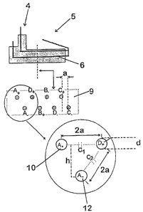
Fig. 6 shows the connector according to the invention in
three degrees of detail, where the upper one in fig. 6
schematically shows part of the connector itself, the
central one shows how the connecting conductors 6 are
mounted in an insulation member 9, and the lower part of
fig. 6 shows a detailed section of the conductor arrange-
ment. As will be seen in fig. 6, the conductors are
placed in two rows or layers. These layers may e.g. form
parallel planes with parallel conductors. The conductors
in the individual layers in the connector may e.g. be ar-
ranged such that these have the same or approximately the
same mutual spacing, as shown in the figure, but may of
course also have different mutual spacings, if this
should be desirable. The two layers may be staggered with
respect to each other, so that the staggering is of a
suitable size. In the embodiment shown in the figure, the
staggering is selected so as to achieve a suitable sym-
CA 02295594 2000-O1-07
WO 99/03172 PCT/DK98/00322
9
metrical conductor arrangement in the connector and
thereby the same coupling between various conductors in
the connector, which will appear from the following.
As will appear from the figure, the conductors of each
pair of conductors are arranged in their respective lay-
ers. As an example, it is shown that the conductors in
the pair of conductors A+, A_ are placed such that the
conductor A+ is placed in one layer, while the conductor
A_ is placed in the other layer. It will also be seen
that, in the example shown, the pole D+ in the pair of
conductors D is placed in the same layer as the pole A+.
The conductors A+, A_ and D, are used below for describing
the conditions in the compensation of crosstalk in a con-
nector, but it should be stressed that other conductors
might be used of course. It should also be noted that the
conductors might of course be placed in other ways in the
connector and yet be distributed such that the two con-
ductors in each pair of conductors are placed in their
respective layers. In the embodiment shown, as will addi-
tionally appear from fig. 6, the centre distance between
all the poles in the individual layers equals 2a, while
the distance between the two layers or rows of conductors
is designated h. A capacitive coupling C1 is schemati-
cally shown between A,~ and D+, while a coupling capacitor
CZ is shown between the pole A_ and the pole D+.
It can be shown that the coupling capacitors C (i.e. C1
or CZ) between two conductors of circular cross-sections
may be calculated by means of the equation:
L~~~~r~~o ~
C = _ (rr~F(L),
~n D+ D-d
d
CA 02295594 2000-O1-07
WO 99!03172 PCT/DK98/08322
where
D is the centre distance (2a) between the conductors,
5 d is the conductor diameter,
L is the length of the conductor,
sr is the relative dielectric constant (permittivity),
10 and
Eo is the dielectric constant in vacuum.
The distance between the two layers may be selected so as
to achieve a suitably small capacitive coupling between
the conductors in the two layers by selecting a suitably
great distance between the two layers. Increasing the ca-
pacitive coupling results in a reduction of the crosstalk
between the layers. For examz~le, when the distance h be-
tween the two layers is selected such that h equals
~.a, the conductors will be positioned entirely symmet-
rically, which means that C1 equals CZ. It is hereby en-
sured that the ~_nfluence from a pole, e.g. D" on two
poles, e.g. A+ arvd A_, in another pair of conductors is
the same on both poles in the pair of conductors. Con-
versely, it thus applies that the influence from the two
poles in a pair of conductors on a pole in another pair
of conductors is neutralized, as the influence of the two
poles is of the same size, but oppositely directed. Com-
pensation of the crosstalk between the conductors in the
connector is achieved hereby.
It is noted that it may be desirable to place the layers
at a mutual distance which is greater than ~.a in order
to achieve full or partial compensation of the crosstalk
which will inevitably occur in other parts of the connec-
CA 02295594 2000-O1-07
WO 99/03172 PCT/DK98/00322
11
tor, e.g. at the contact springs, because of capacitive
couplings between the conductors in these parts. As the
connector typically has to satisfy some specific require-
ments with respect to physical dimensions, it is not
always possible to place the layers at a suitably great
mutual distance. It is described in connection with fig.
7 how this problem is solved.
As mentioned, it is desirable to compensate crosstalk,
which occurs because of capacitive couplings in all parts
of the connector. It is schematically shown in fig. 7 how
compensation of crosstalk, which might e.g. have occurred
in connection with the contact springs, takes place in
the connecting wires. As will be seen, schematically
shown is again part of a connector which is shown on an
enlarged scale at the reference numeral 13. A notch has
been made between the poles A_ and D+ in the connector,
which comprises an insulation member with a first dielec-
tric with the permittivity Er-a. The notch is filled by a
second dielectric 14, as illustrated in the figure. This
material is designated 14 and has another permittivity
which is designated sr_b. It is noted that this second di-
electric may e.g. be atmospheric air or a solid material
having a permittivity which is lower than Er_a. The second
material in the notch shown will give rise to another ca-
pacitive coupling between A_ and D+ compared with the
situation shown in fig. 6 for one thing, and for another
give rise to another capacitive coupling between A_ and
B+, cf. the notation previously used. In the case where
Er_b is selected smaller than ~r_a, these capacitive coup-
lings will thus be reduced compared with the situation
shown in fig. 6.
In this case, the capacitances, cf. the equation stated
above, may be described as
CA 02295594 2000-O1-07
WO 99/03172 PCT/DK98/00322
12
C1 = gr_1 . F ( L ) , and
Cz = ~r_z . F ( L )
where sr_1 and Er-z designate the effective permittivity
between A+ and D+ and A_ and D+, respectively.
Where just a compensation of the crosstalk in the con-
necting conductors 5 in the insulation member 9 is de-
sired, then Er_1 must equal sr_z. When, in the situation
shown, it is additionally desired to compensate crosstalk
between the conductors A_ and D+. which may e.g. be
caused by the capacitive coupling between A_ and D+ be-
cause of their close physical position at the contact
springs, a value of sr_b smaller than sr_a is selected,
however. This will appear more clearly from the follow-
ing.
If e.g. total compensation of crosstalk between D+ and
the pair of conductors A+ and A_ is desired, then it is
necessary to perform compensation of the coupling between
A_ and D+ and of the coupling between A+ and D+, which oc-
cur e.g. because of capacitive coupling at the contact
springs and at the terminals.
The contribution from the coupling between A+ and D+ is
disregarded below, as the coupling between A_ and D+ will
be dominating because of the mutual position of the con
ductors, as will appear from fig. 2. This provides com
pensation when
CA-~D+
Cz + CA_,o+ = Ci => sr-1-Er-2=
CA 02295594 2000-O1-07
WO 99/03172 PCT/DK98/00322
13
which e.g, for a given L, may be realized by suitable se-
lection of Er-1 and Er_2, which reflects the selection of
dielectrics and thereby selection of sr-a and Ez-b.
For reasons of symmetry, this compensation by using the
second dielectric 14 from said compensation of said
crosstalk will also result in an advantageous reduction
of crosstalk between the poles A_, B+ and B_, C+. It is
noted that a suitably low value of the permittivity Er_b
of the second dielectric 14, the mentioned desired com-
pensation of crosstalk can be achieved even when the dis-
tance between the layers is selected smaller than ~.a,
since, in this situation, it is still possible to achieve
compensation of crosstalk between A+ and D+ and between A_
and D+ as well as the desired reduction of crosstalk be-
tween A_, B+'
Fig. 8 shows a further embodiment of a connector accord-
ing to the invention. The figure illustrates that it is
possible to achieve a further reduction of the crosstalk
between individual conductors by placing these at a
greater mutual distance. Since, as mentioned, it is expe-
dient to achieve a reduction of the capacitive coupling
between A_, B+ and B_, C+, the figure shows an example
where the distance between A_, B+ and B_, C+, respec
tively, has been made greater than in the embodiment
shown in figs. 6 and 7. A suitable selection of the per
mittivity may ensure that the desired compensation be
tween the conductors is still achieved, as mentioned
above.
Although the invention has been explained in connection
with specific embodiments of the connecting conductors,
nothing prevents the method from being used in other con-
figurations, for the mere reason that the notch may be
made with many geometrical shapes.