Note: Descriptions are shown in the official language in which they were submitted.
CA 02295840 2000-O1-07
WO 99/03197 PCT/SE98/01347
A~~~~4~~
Field of the invention
The present invention relates to the design of high speed
and high gain operational amplifiers for the use in high
performance switched-capacitor analog circuits, e.g., high
performance analog-to-digital converters. Operational
amplifiers are the most crucial building blocks of analog
circuits. For high perfomance analog-to-digital converters
in wideband radio systems the operational amplifiers set the
limit of speed and accuracy.
Background of the invention
Operational amplifiers are the heart of most voltage-mode
analog circuits. They usually dictate the operation speed
and the accuracy of the switched-capacitor (SC) cicuits.
They also consume most of the power in the SC circuits. High
performance analog-to-digital (A/D) coverters usually use
the SC circuit technique. Therefore, the performance of the
operational amplifiers determines the perfornance of the A/D
converters.
For the SC citcuits, the load is purely capacitive. Usually
single stage operational transconductance amplifiers (OTAs)
are preferred over multi-stage operational amplifiers. In
OTAs, the capacitive load is used to create the single
dominant pole , which usually yields high unity-gain
bandwidth. The DC gain is usually moderate but can be
improved by cascoding. For multi-stage operational
amplifiers, internal miller capacitors and sometimes
resistors are used to split poles and introduce zeros to
compensate for the phase lag and the frequency response can
be independent of the load. However, the unity-gain bandwith
SUBSTITUTE SHEET (RULE 26)
CA 02295840 2000-O1-07
WO 99/03197 PCT/SE98/01347
2
is usually lower than the single-stage OTAs, though the DC
gain is higher due to the cascading of more stages. For high
speed A/D converters, usually single-stage architectures are
preferred in that it is possible to achieve a single-pole
settling and to have a very wide bandwidth. However, the
gain is usually not enough for high accuracy A/D converters.
In for example the document US-A-4 749 956 is shown a fully-
differential operational amplifier for MOS integrator
circuits, where the operational amplifier has one cascode
transistor pair in the P-branch and one cascode transistor
pair in the N-branch, see figure 5 in the said document.
Summary of the invention
ThF- aim of the invetion is to increase the gain without
suffering the speed and that may be achieved by designing a
high speed and high gain operational amplifier for the use
in high performance switched-capacitor analog circuits,
e.g., high performance analog-to-digital coverters. The
invented operational amplifier is a single-stage operational
transconductance amplifier type with single cascode for the
N-type transistors and double cascode for the P-type
transistors. With reference to the cited document there
should be a single-cascode in the N- and P-branches. The
invention may also comprise a cotinuous-time common-mode
feedback. With this design of the invention , high speed and
high gain can be maintained with a large phase margin to
guarantee the stability.
Brief description of the drawings
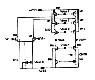
Figure 1 is schematic view of the invented operational
tranconductance amplifier OTA.
CA 02295840 2000-O1-07
WO 99/03197 PCT/SE98/01347
3
Figure 2 is a schematic view of the common-mode feedback
circuit according to the embodiment.
Figure 3 shows a simulated frequency response of the OTA
according to the invention.
Detailed description of the preferred embodiments
The operational amplifier shown in figure 1 is a folded-
cascode OTA. Unlike coventional OTAs a double cascode is
used in the P-branch to increase the gain without much speed
penalty.
Transistors MO and M1 are the input devices and a transistor
M12 provides bias current for them. Input signals Vin+ and
Vin- are applied to the gates of transistors MO and M1,
respectively. Transistors M2 and M3 are bias transistors for
the P-branch. Transistors M4 and M5 and the first cascode
transistor pair in the P-branch and transistors M10 and M11
are the second cascode transistor pair in the P-branch.
Transistors M6 and M7 are bias transistors for the N-branch
and at the same time they provide a means to control the
common-mode component via a signal CMFB generated in a
common-mode feedback circuit. Transistors M8 and M9 are the
cascode transistor pair in the N-brach. Vout+ and Vout- are
the fully differential outputs. VbiasO is the bias voltage
for transistor M12, Vbiasl is the bias voltage for
transistors M8 and M9, Vbias2 is the bias voltage for
transistors M10 and M11, Vbias3 is the bias voltage for
transistors M4 and M5, and Vbias4 is the bias voltage for
transistors M2 and M3. AVCC and AVSS are the supply voltages
usually having values of 5 and OV, respectively.
The invented operational amplifier shown in figure 1 is a
CA 02295840 2000-O1-07
WO 99/03197 PCT/SE98/01347
4
single-stage OTA-type oprational amplifier and the unity-
gain bandwidth is given by: fu = _1 . g"""
2n C
where $min iS the transconductance of the input transistors
MO and M1, and CL is the load capacitance of the OTA.
Suppose the frequence of the parasitic poles formed at the
sources of the cascode transistors are considerably larger
than the dominant pole frequence, a single-pole settling
results. The settling error in unity-gain buffer
configuretion is given by B. Kamth, R. Meyer and P. Gray,
20 "Relationship between frequency response and settling time
of oprational amplifiers", IEEE J. Solid-State Circuits,
vol. SC-9. Dec. 1974, pp. 347-352 b ~V _ ADc
y V 1-EA 'exp(-2lt~fu~t),
DC
where AD~is the DC gain of the oprational amplifier.Suppose
a 12-bit accuracy is needed. The operational amplifier needs
to settling within a half clock sampling period with a 12
2 12
bit accuracy and the relation will be : exp (-2r ~ fu ~ t) <
and thus : fu > li4 = Ol T = ~ = 2.8 ' fsQ,~ptt ,
where T is the sampling period andf is the sampling
sornprc
frequency. The unity gain bandwidth must be three times
larger than the sample frequence to guarantee a 12-bit
settling accuracy.
Considering the parasitic poles and the different
surroundings for the OTA during different clock phases,
there will be required that the unity-gain bandwidth will be
at least six times larger than the sample frequency. Suppose
a sampling frequence of 50 Mhz, then the unity-gain
bandwidth should be over 300 Mhz.
_ _-_.___.._
CA 02295840 2000-O1-07
WO 99/03197 PCTISE98/Q1347
The smaller the load capacitance is, the larger unity-gain
bandwidth will be. However,there are two advers effects of
using small load capacitance. The thermal noise power and
other noise power is inversely proportional to the sampling
5 capacitance. Also the non-dominant poles can decrease the
phase margin, if the non dominant poles are not so far apart
from the dominant pole that is inversely proportional to the
load capacitance. Therefore the load capacitance will be
chosen 2~ 4 pF. With this large sampling capacitance, the
thermal noise does not limit the dynamic range of 12 bits if
the peak input signal is larger than 0.5 V.
As a general rule, the phase margin should be larger than a5
deg for SC applications. With this large load capacitance,
the phase margin is easy to guarantee.
The accuracy is directly related with the DC gain of the OTA
and its capacitive surroundings. Suppose a 12-bit accuracy
is needed, a rough estimation of DC gain is given by:
ADS>2~212=78dB.
Considering the design margin, the DC gain is reqiured to b'
larger than: 78 + 3 - 81 dB. To achieve this high gain, it
is necessary to use cascode technique. Since the gain and
output resistance of a PMOS transistor is considerably
smaller than the gain and output resistance of an NMOS
transistor, double cascodes are used for the upper branch as
sho4m in figure 1. The DC gain is given by:
ADC ~ groin ~ro6 ' Abt3 ~~ ro2 ' Aht : ' Abtlo~
where rob and t'o2 are the output resistance of the transistors
rI5 and M2, respectively, A M8 ' AMT and AMJD are the gain of
the transistors M5, M4 and M10, respectively. The drawback
CA 02295840 2000-O1-07
WO 99/03197 PCT/SE98/01347
6
is the limited output voltage range. However, it is of
benefit to reduce the voltage swing to reduce distortion due
to the sampling. Since the mobility in NMOS transistors is
more than 4 times larger than that in PMOS transistors in
certain aviable CMOS process, it is a good choice to design
the common-mode voltage as low as possible to reduce the
switch-on resistance of NMOS switches. The common-mode
voltage is set to be 2V. The output voltage can swing more
than +/- 1.2V without degradation in performance.
Shown in figure 2 is the common-mode feedback circuit.
Transistors M35 and M36 are the input devices of the common-
mode feedback circuit and their gates are connected with the
input voltages Vin+ and Vin-, respectively, which are the
fully-differential outputs Vout+ and Vout- of the
operational amplifier of figure 1. Transistors M33 and M34
provide bias currents for the input devices M35 and M36.
Resistors I37 and I38 are used to generate the common-mode
voltage in the fully differential input voltages at the gate
of transistor M66. Noticable is that the common-mode voltage
is level-shifted due to the gate-source voltage of
transistors M35 and M36. The common-mode input voltage Vcm
is applied to the gate of transistor M67 via transistor M39
and level-shifted by the gate-source voltage of transistor
M39. Transistor M40 provides the bias current for transistor
M39. The difference between the voltages applied at the
differential pair M66 and M67 i.e., the level-shifted
common-mode voltage in the fully differential signals and
the level-shifted common-mode input voltage is used to
generate the common-mode control signal CMFB used in the
operational amplifier of figure 1. Transistors M68 and M69
are the loads for the differential transistor pair M66 and
CA 02295840 2000-O1-07
WO 99/03197 PCT/SE98/01347
7
M67 and the current in transistor M69 is used to control the
common-mode voltage in the operational amplifier of figure 1
via the signal CMFH. Transistor M64 is the bias transistor
for the differential pair M66 and M67 and transistor M65 is
the cascode transistor for transistor M64. VbiasO is the
bias voltage for transistors M33, M34, and M40, Vbias3 is
the bias voltage for transistor M65, and Vbias4 is the bias
voltage for transistor M64. AVCC and AVSS are the supply
voltages having values of 5 and OV, respectively.
To verify the performance a SPICE simulation is carried out
within the CADENCE platform. An optimization of DC
operation points is prioritized to make the circuit less
sensitive to process variation. The optimization is carried
out in such a way that there is enough source-drain voltage
to guarantee all the transistors iri saturation region even
when there is a considerable change in threshold voltage and
transistor dimension. The simulation result is shown in
ffigure 3, where both the amplitude and the the phase
response are shown.
To check the robustness of the circuit the bias current is
varied by 200, and both the input and the output common-mode
voltage are varied from 1.8 to 2V. Under all these
variations, the DC gain is larger than 83dB, the unity gain
bandwidth is larger than 400Mhz, and the phase margin is
around 60deg with a 4-pF capacitance, as seen in figure 3.
The performance of the OTA is summarized in table 1.
While the foregoing description includes numerous details
and specificities, it is to be understood that these are
merely illustrative of the present invention, and are not to
be construed as limitations. Many modifications will be
CA 02295840 2000-O1-07
WO 99/03197 PCT/SE98/01347
8
readily apparent to those skilled in the art, which do not
depart from the spirit and the scope of the invention, as
defined by the appended claims andtheir legal equivalents.
10
20
_.T __ _
CA 02295840 2000-O1-07
WO 99/03197 PCT/SE98/01347
Table 1: Summary of the performance of the OTA
2-pF capacitive load 4-pF capacitive load
power dissipation C~ 25 mW 25 mW
SV
DC gain (dB) 85 ~ 85 dB
Unity-gain bandwidth 750 MHz 420 MHz
Phase maigin 49 deg 66 deg
Slew rate (positive 340 Vlus ~ 180 V/us
transition)
Slew rate (negative 530 V/us ' 270 Vlus
transition)
CMRR (matched) > 100 dB ! > 100 dB~
PSRR (positive supply) 66 dB 66 dB
PSRR (negative supply) 69 ~ 69 dB