Note: Descriptions are shown in the official language in which they were submitted.
CA 02296026 2000-O1-10
WO 99/03087 PCT/US98/13935
1
BONDED ACTIVE MATRIX ORGANIC LIGHT EMITTING DEVICE
DISPLAY AND METHOD OF PRODUCING THE SAME
Cross Reference To Related Patent Application
This application relates to and claims priority on provisional application
serial
number 60/052,357, filed July 11, 1997 and entitled "Bonded Active Matrix
Organic
Light Emitting Display."
Field of the Invention
The present invention relates to organic light emitting devices. In
particular, the
present invention relates to a method of sealing an organic light emitting
device plate and
an active matrix plate sealed together to create a high performance video
display.
Background of the Invention
Light emitting devices, which may be generally classified as organic or
inorganic,
are well known in the graphic display and imaging art. Among the benefits of
organic
light emitting devices are high visibility due to self emission, as well as
high power
efficiency, and ease of handling of the solid state devices. Organic light
emitting display
devices may have practical application for television and graphic displays, as
well as in
digital printing applications.
An organic light emitting display device is typically a laminate formed on a
substrate such as soda-lime glass. A light-emitting layer of a luminescent
organic solid,
as well as adjacent semiconductor layers, are sandwiched between a cathode and
an
anode. The semiconductor layers may be hole-injecting and electron-injecting
layers.
The light-emitting layer may be selected from any of a multitude of light
emitting organic
solids. The light-emitting layer may consist of multiple sublayers.
When a potential difference is applied across the cathode and anode, electrons
from the electron-injecting layer, and holes from the hole-injecting layer are
injected into
the light-emitting layer. They recombine, emitting light.
CA 02296026 2000-O1-10
WO 99/03087 PCT/US98I13935
2
In a typical matrix-addressed organic light emitting display device, numerous
light emitting devices are formed on a single substrate and arranged in groups
in a regular
grid pattern. Several light emitting device groups forming a column of the
grid may
share a common cathode, or cathode line. Several light emitting device groups
forming
a row of the grid may share a common anode, or anode line. The individual
light
emitting devices in a given group emit light when their cathode and anode are
activated
at the same time. Activation may be by rows and columns or in an active matrix
with
individual cathode or anode pads.
Organic light emitting devices have a number of beneficial characteristics.
These
include a low activation voltage (about 3 to 6 volts), fast response when
formed with a
thin light-emitting layer, and high brightness in proportion to the injected
electric current.
By changing the kinds of organic solids making up the light-emitting layer,
many
different colors of light may be emitted, ranging from visible blue, to green,
yellow, and
red. Organic light emitting devices are currently the subject of aggressive
investigative
efforts.
Organic light emitting devices need to be protected from the atmosphere. The
light emitting organic material in the light-emitting layer can be highly
reactive. The
material is susceptible to water, oxygen, etc. Moisture and oxygen may cause a
reduction
in the useful life of the light emitting device. The cathode and anode may
also be
affected by oxidation. One disadvantage of oxygen and moisture penetration
into the
interior of the organic light emitting device is the potential to form metal
oxides at the
metal-organic interface. These metal oxide impurities may allow separation of
the
cathode or anode and the organic in a matrix addressed OLED, especially the
oxidation
sensitive cathode, such as, Mg-Ag or Al-Li. This can result in the formation
of dark non-
emitting spots (i.e., no illumination) because no current flows through the
area of the
separation.
As discussed above, exposing a conventional light emitting device to the
atmosphere shortens its life. To obtain a practical, useable organic light
emitting device,
it is necessary to protect the device, so that water, oxygen, etc., do not
infiltrate the light-
emitting layer.
Methods commonly employed for protecting or sealing inorganic light emitting
devices are typically not effective for sealing organic light emitting
devices. Resin
CA 02296026 2000-O1-10
WO 99/03087 PCT/US98/13935
3
coatings that have been used to protect inorganic light emitting devices are
not suited for
organic light emitting devices. The moisture and oxygen permeability of even
the best
organic adhesives is far too high, and the organic light emitting device often
degrades due
to chemical or mechanical effects.
The present invention is directed to a method for processing active matrix
organic
light emitting device displays with nontransparent substrates, such as, for
example,
silicon. Non-transparent substrates provide a low cost method for obtaining
active matrix
circuitry and high performance drivers, along with an opportunity to integrate
other
system or display functions into small-medium size displays. The organic light
emitting
device can be fabricated using this method without the need for silicon
substrate
planarization, and with optimized organic light emitting device structures on
an
independent glass plate.
Objects of the Invention
It is therefore an object of the present invention to bond an OLED plate and
an
active matrix plate together to create a high performance video display.
It is another object of the present invention to provide a method for
processing
active matrix OLED displays with non-transparent substrates such as silicon.
It is a further object of the present invention to provide a low cost method
for
obtaining active matrix circuitry and high performance drivers, along with an
opportunity
to integrate other system or display functions into small to medium sized
displays.
It is still another object of the present invention to provide a method for
fabricating an active matrix OLED without the need for silicon substrate
planarization,
and with optimized OLED structures on an independent glass plate.
It is still yet another obj ect of the present invention to provide a method
of sealing
the active matrix substrate and the OLED plate together to bring the two
plates into
intimate contact.
Additional objects and advantages of the invention are set forth, in part, in
the
description which follows and, in part, will be apparent to one of ordinary
skill in the art
from the description and/or from the practice of the invention.
CA 02296026 2000-O1-10
WO 99/03087 PCT/IJS98113935
4
Summary of the Invention
The present invention is directed to a method of forming an active matrix
organic
light emitting device display. The method includes the steps of providing an
organic
light emitting plate assembly, providing an active matrix plate assembly, and
sealing the
organic light emitting plate assembly to the active matrix assembly.
The active matrix plate assembly may include a substrate, drive circuitry
formed
thereon, and at least one pixel pad. The at least one pixel pad may be formed
from an
electron injector material. The electron injector material may be selected
from one of the
group consisting of Mg+Al, Al+Li, LiF/Al and CsC.
The method may further include the step of cleaning the at least one pixel pad
prior to the step of sealing the organic light emitting plate assembly to the
active matrix
plate assembly. The cleaning step may include the step of ion beam cleaning of
at least
one pixel pad.
The organic light emitting plate assembly may include a substrate, a conductor
layer and at least one OLED layer. The organic light emitting plate assembly
may further
include at least one color filter.
The step of sealing the organic light emitting plate assembly to the active
matrix
plate assembly may comprise the steps of locating the organic light emitting
plate
assembly and the active matrix plate assembly in a sealing environment, and
securing a
perimeter of the organic light emitting plate assembly to a perimeter of the
active matrix
plate assembly. The environment may be one of a vacuum environment, an inert
gas
environment and a moisture absorbing gas environment.
The step of securing the perimeter of the organic light emitting plate
assembly to
the perimeter of the active matrix plate assembly may include sealing the
perimeter ofthe
organic light emitting plate assembly to the perimeter of the active matrix
plate assembly
with a fused metal seal. Alternatively, the step of securing the perimeter of
the organic
light emitting plate assembly to the perimeter of the active matrix plate
assembly may
include sealing the perimeter of the organic light emitting plate assembly to
the perimeter
of the active matrix plate assembly with a polymer. The polymer may be a low
moisture
diffusivity polymer. The low moisture diffusivity polymer may be a two-
component
adhesive, or cured by heat or ultraviolet light.
3
coatings that have been used to
CA 02296026 2000-O1-10
WO 99/03087 PCT/US98I13935
The sealing of the organic light emitting plate assembly to the active matrix
plate
assembly may be done in a low-pressure inert environment by bringing the
surfaces of
the two assemblies into intimate contact, and may include the application of
pressure
and/or heat.
S The present invention is also directed to a high performance display
including an
organic light emitting device, an active matrix substrate; and an assembly for
bonding the
organic light emitting device to the active matrix substrate. The organic
light emitting
device may include a substrate, at least one conductor formed on the
substrate, and a first
insulator layer formed on the conductor. The organic light emitting device may
include
a color filter disposed between the substrate and the conductor. The organic
light
emitting device may include a color conversion filter disposed between the
substrate and
the conductor.
The substrate may be a thin transparent material. The active matrix substrate
may
include a second substrate, independently addressed pixel pads, and driver
circuitry. The
active matrix substrate may be fabricated on a non-transparent substrate.
The independently addressed pixel pads may be produced from an electron
injector material with high vertical conductivity and low horizontal
conductivity. The
independently addressed pixel pads make contact with the organic light
emitting device.
The independently addressed pixel pads may be elevated by at least one
insulator. The
independently addressed pixel pads may be elevated by stacking the pixel pads
on top of
at least one lower silicon circuit structure.
The organic light emitting device and the active matrix substrate may be
sealed
together in an inert or moisture-reactive gas environment. The organic light
emitting
device and the active matrix substrate may be sealed together using a fused
metal seal.
The organic light emitting device and the active matrix substrate may be
sealed
together using at least one low moisture diffusivity polymer. The low moisture
diffusivity polymer may be a non-solvent containing epoxy or acrylic. The low
moisture
diffusivity polymer may be a W or heat cured adhesive.
It is to be understood that both the foregoing general description and the
following detailed description are exemplary and explanatory only, and are not
restrictive
of the invention as claimed. The accompanying drawings, which are incorporated
herein
by reference, and which constitute a part of this specification, illustrate
certain
CA 02296026 2000-O1-10
WO 99103087 PCT/US98/13935
6
embodiments of the invention, and together with the detailed description serve
to explain
the principles of the present invention.
Brief Description of the Drawings
Fig. 1 is a side view of an active matrix organic light emitting display
device prior
to assembly according to the present invention;
Fig. 2 is a side view of the active matrix organic light emitting display
device in
an assembled state according to the present invention; and
Fig. 3 is a side view of an active matrix organic display device prior to
assembly
with OLED stacks on both assemblies according to the present invention.
Detailed Description of the Preferred Embodiments
Reference will now be made in detail to a preferred embodiment of the present
invention, an example of which is illustrated in the accompanying drawings.
The present
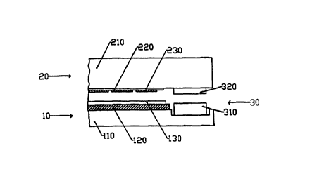
invention is directed to an improved light emitting device 1 that includes an
organic light
emitting plate assembly 10 that is secured to an active matrix plate assembly
20.
The organic light emitting plate assembly 10 includes a substrate 110. The
substrate 110 is preferably formed from a transparent material such as, for
example,
mylar or glass. It, however, is contemplated by the inventors of the
prevention that other
suitable materials may be used for forming the substrate 110. This substrate
might be
particularly flat and flexible. A conducting layer 120 is formed on the
substrate 110. The
conducting layer 120 is preferably formed from indium tin oxide (ITO). A
planar OLED
stack 130 is formed on the conducting layer 120. The OLED stack 130 may
include an
electron injector material with high vertical conductivity and low horizontal
conductivity.
The electron injector material may be LiF.
The organic light emitting plate assembly 10 may include at least one color
changing filter 140. The at least one color changing filter 140 is probably
located
between the substrate 110 and the conducting layer 120. The surfaces of the
OLED
materials and the filters should be smooth and nearly planar to ensure proper
orientation
with the plate assembly 20 after fabrication. Alternatively, the OLED
materials may be
patterned into red, green and blue emitters to produce a color display. A
color display
CA 02296026 2000-O1-10
WO 99/03087 PCT/US98l13935
7
may also be produced by patterning part of the color OLED emitter on one
substrate and
the other two color OLED emitters on another substrate, as shown in Fig.3.
This makes
direct shadow masking of direct color organic light emitting display devices
more simple.
The active matrix plate assembly 20 includes a substrate 210. The substrate
210
S is preferably formed from silicon or another suitable substrate material.
The active
matrix plate assembly 20 further includes driver circuitry and other system
related
electronics 220. The matrix plate assembly 20 preferably includes CMOS drivers
and
transistor and capacitor cells.
The active matrix plate assembly 20 also includes at least one pixel pad 230.
Each pixel pad 230 corresponds to a pixel on the display device and is
independently
addressable. Each pixel pad 230 is preferably formed from a good quality
electron
injector material. The electron injector material may be formed from Mg+Ag,
Al+Li,
LiF/Al or CSC. The present invention is not limited to these materials or
polarlity;
rather, it is contemplated that other suitable injector materials may be used.
Each pixel
pad 230 must be sized such that it contacts the OLED stack 130 when the
organic light
emitting plate assembly 10 is secured to the active matrix plate assembly 20.
A thickness
of between 0.5-10 microns is acceptable for this purpose. The pixel pads 230
may be
elevated by other structures, such as, for example, a thick insulator and a
via plug.
Additionally, the pixel pads 230 may be stacked on top of lower silicon
circuit structures.
Additionally, a shallow trench might be etched for the seal.
A sealing assembly 30 is provided to secure the organic light emitting plate
assembly 10 to the active matrix plate assembly 20. The sealing assembly 30
preferably
includes a first sealing assembly 310 formed on the organic light emitting
plate assembly
10 and a second sealing assembly 320 formed on the active matrix plate
assembly 20.
The sealing assembly 30 may be a fused metal seal. The sealing assembly 30 is
not
limited to a metal seal; rather, low moisture diffusing polymers including but
not limited
to a non-solvent containing a UV or heat cured adhesive may be used.
The method of sealing the organic light emitting plate assembly 10 to the
active
matrix plate assembly 20 will now be described.
The active matrix plate assembly 20 is formed by fabricating the driver
circuitry
and other system related electronics 220 on the substrate 210. The active
matrix plate
assembly 20 may be fabricated using known techniques. The organic light
emitting plate
CA 02296026 2000-O1-10
WO 99/03087 PCTNS98/13935
8
assembly 10 is formed by fabricating an OLED structure on a substrate 110. The
OLED
structure may be formed using known techniques. The OLED structure includes
the
conducting layer 120, the planar OLED stack 130. The OLED structure may
further
include at least one color changing filter 140.
A first sealing assembly 310 is formed along the perimeter of the organic
light
emitting plate assembly 10. A second sealing assembly 320 is formed along the
perimeter of the active matrix plate assembly 20. The plate assemblies 10 to
20 are
located in a vacuum or inert gas environment. The first and second sealing
assemblies
310 and 320 are then brought into contact. After sealing, the light emitting
device 1 is
removed from the low-pressure environment. Under the influence of atmospheric
pressure, the plate assemblies 10 to 20 move into intimate contact such that
each pixel
pad 230 is in contact with the organic light emitting plate assembly 10. This
works when
the pressure of the inert gas inside is sufficiently below the ambient
pressure.
It is important to avoid air and moisture exposure between the preparation of
the
plate assemblies 10 to 20 and the sealing operation. Accordingly, the entire
fabrication
process may take place in a vacuum or an inert gas environment. Alternatively,
a
moisture reactive gas may be employed to keep the surfaces of the plate
assemblies 10
to 20 free of moisture before and during the sealing process. Non-vacuum
sealing can
best be performed by applying pressure in the center of one or both of the
plastic
assemblies 10 to 20. Alternatively, one or both of the plastic assemblies 10
to 20 may
be bowed prior to sealing.
The pixel pads 230 may be ion bean cleaned prior to sealing the plastic
assemblies
10 to 20 together.
While the invention has been described in conjunction with specific
embodiments
thereof, it is evident that many alternatives, modifications and variations
will be apparent
to those skilled in the art. For example, the above-described method may be
used with
other TFT active matrix substrates when larger displays are fabricated. This
permits
more processing options and the ability to build transport displays. The above-
described
method can also be used for passive OLED fabrication where the election
injector/conductor lines and ITO/OLED lines cross over at the OLED light
generating
pixels. Additionally, the OLED structure can be built on either the
transparent conductor
side or the active matrix side of the plate assembly 10. If the OLED structure
is reversed
CA 02296026 2000-O1-10
WO 99/03087 PCTIUS98/13935
9
with the hole injector on top, then a gold interface layer can be used on the
pixel pads
230. Furthermore, a thin Mg+Ag, A1+Li, LiF/A1 or CsC layer can act as a
transparent
electron injector on the transport ITO layer. Accordingly, the preferred
embodiments of
the invention as set forth herein are intended to be illustrative, not
limiting. Various
changes may be made without departing from the spirit and scope of the
invention as
defined in the following claims.