Note: Descriptions are shown in the official language in which they were submitted.
CA 02296090 2004-05-11
- 1 -
PRESSURE SENSOR AND METHOD OF
MANUFACTURING THE SAME
Technical Field
s This invention relates to a pressure sensor
which permits an ultra fine element to be formed easily,
and which is optimumly used to determine various kinds of
pressures in the body, such as a blood pressure, etc. by
incorporating the pressure sensor in a catheter and a.
to guide wire inserted into the body, or by directly
inserting the pressure sensor into a blood vessel and the
like, and to form a photodetector type pressure sensor
for a capillary and the like; and a method of
manufacturing the same.
Background of the Invention
A pressure sensor of related art utilizing a
photodetecting principle by using an optical fiber does
not utilize an electric signal, such as a piezoresistive
2o signal, etc. Accordingly, this pressure sensor rarely
receives environmental disturbance ascribed to the
electricity and magnetism, and has a possibility of being
applied to the interior of an organism (refer to Japanese
Patent Publication 57-207838 published on 20-12-1982,
Japanese Patent Laid-Open No. 235731/1986 and Japanese
Patent Laid-Open No. 201196/1996).
CA 02296090 2000-O1-12
-2-
The pressure sensors using an optical fiber are
roughly classified under pressure sensors of the type
which has a cantilever beam type silicon structure fixed
to a side surface of an optical fiber with a mirror, which
faces an end surface of the optical fiber, fixed to a front
end of the beam, and which utilizes the variation of the
quantity of reflected light caused by the variation of
the position of the mirror due to the flexure of the beam
ascribed to pressure variation, and pressure sensors of
the type which has on a front end of an optical fiber a
silicon structure having a total reflection mirror
serving also as a movable diaphragm, and joined to a glass
structure and fixed to an end surface of the optical fiber
by using a bonding agent, and which measures an amount
of flexure of the diaphragm as variation of the intensity
of the light.
However, in a pressure sensor of the type which
utilizes a side surface of an optical fiber, a side wall
is tapered to form a large etching window. This causes
the dimensions of a pressure sensor portion to increase,
and also makes it difficult to insert the pressure sensor
into a working channel of a catheter and an endoscope,
and obtain a pressure sensor capable of being inserted
directly into a capillary, such as a blood vessel and the
like.
There are related techniques comprising a method,
as a method of fixing a total reflection mirror serving
CA 02296090 2000-O1-12
-3-
also as a movable diaphragm to a front end of an optical
fiber, of forming a fine ring-shaped bonding agent layer
on a posiresist layer, which is provided on a glass plate,
by exposing the posiresist layer via an A1 mask,
transferring the bonding agent layer onto a front end of
an optical fiber, fixing the resultant layer to a
diaphragm formed and held in a frame of a silicon substrate
via a holding portion, and cutting off the holding portion
with a laser beam. However, in this method, an efficiency
of transferring the bonding agent layer onto the front
end of the optical fiber is low, and it takes much time
and labor to separate the diaphragm from the silicon
substrate by cutting off the holding portion with a laser
beam. Therefore, this method is inferior in the
manufacturing efficiency of a pressure sensor and the
yield thereof.
The present invention has been devised so as to
eliminate the drawbacks, such as a low yield on the
manufacturing of a pressure sensor portion, or a low yield
on the connecting of a pressure sensor and an optical fiber
together which are encountered in an optical fiber type
pressure sensor of related art capable of being used in
the interior of an organism such as a blood vessel, etc.
and a capillary.
Disclosure of the Invention
The present invention provides a pressure sensor
CA 02296090 2000-O1-12
-4-
characterized in that a reflective type movable diaphragm
unit which has a mesa portion of a circular, thick Si02
film, and a light reflecting mirror portion formed of a
thin A1 film in the center of a diaphragm portion formed
of a circular, thin SiOz film, and which has a ring-shaped
spacer serving also as a bonding agent layer at a
circumferential edge section of the diaphragm portion,
is fixed in a sealed state to a front end, which has a
half mirror layer thereon, of an optical fiber of not
larger than 125 um in diameter, the diaphragm portion
having a cross-sectionally substantially semicircular
part.
The present invention further provides a method of
manufacturing pressure sensors, characterized in that
the method includes a step of accumulating Si02 layers
on a front surface of a silicon substrate and forming mesa
portions by circularly leaving the Si02 layers, a step
of accumulating on a rear surface of the silicon substrate
SiOz layers as masks for separating reflective type
movable diaphragms from the silicon substrate, a step of
forming diaphragm portions by further accumulating Si02
layers on the front surface of the silicon substrate, a
step of forming light reflecting mirror portions by
accumulating A1 layers on the mesa portions, a step of
forming around the diaphragm portions spacers serving
also as adhesive layers and comprising polyimide, a step
of separating the reflective type movable diaphragm units
CA 02296090 2000-O1-12
-5-
from the silicon substrate, a step of forming half mirror
layers on front ends of optical fibers, a step of fixing
the reflective type movable diaphragm units to the front
ends of the optical fibers by inserting the reflective
type movable diaphragm units into capillaries so that the
end surfaces of the diaphragm units and those of the
optical fibers are opposed to each other, bringing the
reflective type movable diaphragm units and optical
fibers into close contact with each other by microbeads
and other optical fibers inserted from the other ends of
the capillaries, and turning the polyimide layers into
bonding agents by heating the diaphragm units, and a step
of withdrawing the optical fibers from the capillaries,
the step of forming the diaphragm portions including a
step of accumulating Si02 layers in annular grooves
provided in the front surface of the silicon substrate
and thereby forming cross-sectionally substantially
semicircular parts.
The present invention still further provides a
method of manufacturing pressure sensors, characterized
by forming reflective type movable diaphragm unit and
optical fibers by using the above-mentioned initial step
to the step of forming half mirror layers; inserting the
above-mentioned movable diaphragm unitsinto capillaries
so that the end surfaces of the diaphragm units and those
of the optical fibers are opposed to each other; bringing
the reflective type movable diaphragm units and optical
CA 02296090 2000-O1-12
-6-
fibers into close contact with each other by microbeads
and other optical fibers inserted from the other ends of
the capillaries; turning the polyimide layers into
bonding agents by heating the diaphragm units, whereby
the reflective type movable diaphragm units are fixed to
the front ends of the optical fibers.
Brief Description of the Drawings
Fig. 1 is a sectional view of an example of a pressure
sensor;
Figs. 2a to 2h are explanatory drawings showing
examples of steps of manufacturing reflective type
movable diaphragm units;
Figs . 3a to 3d are explanatory drawings showing an
example of a process for bonding a reflective type
diaphragm unit and an optical fiber to each other; and
Fig. 4 is a sectional view of another example of
a pressure sensor.
Mode for Carrying Out the Invention
In the pressure sensor according to the present
invention, a reflective type movable diaphragm unit
having a mesa portion of a thick SiOZ film and a light
reflecting mirror portion of a thin A1 film in the center
of a corrugated type diaphragm portion formed of a
circular, thin film of Si02, and a spacer serving also
as an adhesive layer and comprising a thick film of
CA 02296090 2000-O1-12
polyimide at a circumferential edge section of the
diaphragm portion is fixed in a sealed state to a front
end, which has a half mirror layer of ZnS, of an optical
fiber of not larger than 125 um in diameter. An example
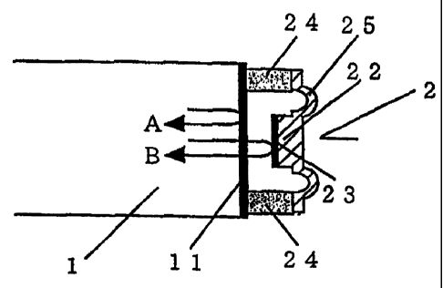
of this pressure sensor is shown in Fig. 1. A reference
numeral 1 denotes an optical fiber, 11 a ZnS layer (half
mirror layer) thereof, 2 a reflective type movable
diaphragm unit, 25 a Si02 layer (corrugated type diaphragm
portion) thereof, 22 a Si02 layer (mesa portion) thereof,
23 an A1 layer (light reflecting mirror portion) thereof,
and 24 a polyimide layer (spacer serving also as an
adhesive layer) thereof.
The manufacturing of the reflective type movable
diaphragm unit of this pressure sensor can be done, for
example, bythefollowing method. Namely, thereflective
type movable diaphragm unit of the pressure sensor can
be manufactured as shown in the examples of steps in Figs.
2a to 2h, by a step (a, b) of forming mesa portions 22
by digging annular grooves 26 for corrugated diaphragm
portions in a front surface of a silicon substrate 3,
accumulating Si02 layers on central circular portions
defined by the grooves 26, and leaving the SiOZ layers
circularly, a step (a, b) of accumulating on a rear surface
of the silicon substrate 3 Si02 layers as masks 31 for
separating reflective type movable diaphragm units 2
individually from the silicon substrate 3, a step (c, d)
of forming corrugated type diaphragm portions 25 by
CA 02296090 2000-O1-12
_8_
further accumulating Si02 layers on the front surface of
the silicon substrate 3 including the grooves 26, a step
(e, f) of forming light reflecting mirror portions 23 by
accumulating A1 films on the mesa portions 22, a step (e,
f ) of forming spacers serving also as adhesive layers 24
and comprising polyimide on circumferential edge
sections of the corrugated type diaphragm portions 25,
and a step (g, h) of separating the reflective type movable
diaphragm units 2 from the silicon substrate 3.
The manufacturing steps illustrated in Fig. 2 are
the manufacturing steps used in a case where a plurality
of reflective type movable diaphragm units are formed on
one silicon substrate, and then separated therefrom.
Accordingly, a plurality of reflective type movable
diaphragm units can be formed at once by using a silicon
substrate of a large area, and, moreover, the
manufacturing steps themselves are simple. Therefore,
the through-put and yield become high, and a production
efficiency can be improved easily.
The bonding of an optical fiber 6 of not larger than
125 um in diameter having a half mirror layer of ZnS at
a front end thereof to a front end of a reflective type
movable diaphragm unit manufactured by the steps of Fig.
2 can be done, for example, by the following method.
Namely, as shown the examples of steps in Figs . 3a to 3d,
the method includes a step (a) of inserting the
above-mentioned reflective type movable diaphragm unit
CA 02296090 2000-O1-12
_g_
2 and an optical fiber 1 of not larger than 125 um in
diameter having a half mirror layer of ZnS at a front end
thereof into a capillary 4 so that the ends thereof are
opposed to each other, and inserting a microbead 5 and
another optical fiber 6 for a bonding purpose from the
other end of the capillary thereinto, a step (b) of
bringing the reflective type movable diaphragm unit 2 and
optical fiber 1 into close contact with each other by the
microbead 5 and bonding optical fiber 6, and heating the
diaphragm unit, a step (c) of fixing in a sealed state
the diaphragm unit to the optical fiber 1 with a polyimide
layer 24 turned into an adhesive layer by the heating
operation, and a step (d) of removing the silicon
substrate 3 by etching the same.
Referring to Fig. 2, the thickness of the silicon
substrate 3 in use is suitably determined in the step of
bonding the reflective type movable diaphragm unit 2 and
optical fiber 1 together. When the silicon substrate is
too thin, the handling thereof with respect to the
capillary 4 becomes difficult, and, when it is too thick,
it is tapered in the step of separating the reflective
type movable diaphragm unit 2 therefrom, so that the
diaphragm unit cannot be inserted into the capillary 4.
Anot greater than 5 mm silicon substrate is used generally,
25 a not greater than 1 mm silicon substrate particularly,
and a 0. 1 to 0. S mm silicon substrate more particularly.
A both-side polished silicon substrate is used to
CA 02296090 2000-O1-12
-10-
carry out photolithography on both surfaces thereof.
Although a surface direction is not specially limited
when the silicon substrate is removed by a dry etching
method based on a micromachining system directed to the
formation of a semiconductor circuit, it is suitably
determined when wet etching is carried out. In general,
a surface direction of (100) or (110) is used.
Referring to Figs. 2a and 2b, the annular grooves
26, which are dug in the front surface of the silicon
substrate 3, for the corrugated type diaphragm portions
determine the shape of the diaphragm portions 25, and the
shape of the grooves 26 can be determined suitably in
accordance with the residual stress on and the pressure
deformability of the corrugated type diaphragm portions
25. The depth of the annular grooves 26 is 2 to 6 dun,
and preferably 5 um, the width thereof 8 to 12 ~.~m, and
preferably 10 ~.un, and the diameter thereof 71 to 79 um,
and preferably 75um.
The Si02 layers provided on the front surface of the
silicon substrate 3 are to form mesa portions 22 of the
reflective type movable diaphragm units 2, and the
thickness of the layers can be determined suitably in
accordance with the function, etc. of the mesa portions
of preventing the light reflecting mirror portions 23
comprising Al layers from being bent when the diaphragms
are deformed. This thickness is set to not larger than
15 um generally, not larger than 10 um particularly, and
CA 02296090 2000-O1-12
-11-
2 to 5 um more particularly.
Accordingly, a method of forming the mesa portions
22 by circularly leaving the Si02 layers on the front
surface of the substrate can be carried out by
additionally providing a Si02 layer by a suitable system,
such as a CVD system and the like, and removing (a, b)
an unnecessary part of the Si02 layer by a micromachining
system and the like directed to the formation of a
semiconductor circuit in which the SiOz layer is subj ected
to patterning and etching based on photolithography,
whereby the Si02 layers 22 are circularly left.
Referring further to Figs . 2a and 2b, in order that
the Si02 layers provided on the rear surface of the silicon
substrate 3 are used as masks 31 for an etching operation
for separating the reflective type movable diaphragm
units 2 from the silicon substrate 3, the thickness of
the same layers can be determined suitably in accordance
with the etching selectivities of the Si02 and silicon.
This thickness is set to not larger than 2 um generally,
not larger than 1 um particularly, and 0.5 to 1 um more
particularly.
Therefore, forming the masks 31 for an etching
operation by circularly leaving the Si02 layers on the
rear surface of the substrate can be carried out by a
method identical with that used for forming mesa portions
22 on the front surface of the silicon.
As shown in Figs . 2c and 2d, the circular corrugated
CA 02296090 2000-O1-12
-12-
type diaphragm portions 25 comprising SiOZ on the silicon
substrate constitute substantial movable portions.
Therefore, the formation of the diaphragm portions 25 can
be suitably determined in accordance with the pressure
deformability, etc. of the diaphragm portions 21 with
respect to the residual stress at the time of forming the
SiOZ layers . The diaphragm portions can be formed easily,
for example, by thermal CVD, plasma CVD using as a material
TEOS the residual stress of which can be controlled, etc.
The thickness of the circular corrugated type
diaphragm portions 25 comprising Si02 layers can be
determined suitably in accordance with the pressure
deformability of the diaphragm portions working as
diaphragms . This thickness is set to not larger than 5
um generally, not larger than 2 um particularly, and 0.5
to 1 um more particularly.
As shown in Figs . 2e and 2f, the formation of the
light reflecting mirror portions 23 comprising A1 layers
can be carried out by removing unnecessary portions of
the A1 layers, which are provided additionally by a
suitable system, such as vapor deposition, etc., by a
micromachining system directed to the formation of a
semiconductor circuit in which patterning and lift-off
by photolithography are carried out, and thereby
circularly leaving the Al layers . The formation of the
light reflecting mirror portions 23 can also be carried
out by providing A1 layers additionally by a suitable
CA 02296090 2000-O1-12
-13-
system, such as vapor deposition, etc., and etching the
unnecessary portions of the Al layers by utilizing a
photolithographicsystem. Thethicknessof theAllayers
23 can be determined suitably in accordance with the
necessity of the A1 layers of functioning as total
reflection mirrors . This thickness is set to not smaller
than 0.2 um generally, 0.2 to 1 um particularly, and 0.2
to 0.5 um more particularly.
Referring to Figs. 2e and 2f, the formation of the
spacers serving also as adhesive layers 24 and comprising
polyimide which extend around the corrugated type
diaphragm portions 21 is carried out by patterning the
polyimide in the same manner as in a micromachining system
directed to the formation of a semiconductor circuit in
which the patterning of regular photoresist is done. The
conditions for a curing operation carried out after the
patterning of the polyimide can be determined suitably
due to the necessity of utilizing the polyamide as an
adhesive layer for the bonding of the optical fiber 1.
The curing operation is carried out at not higher than
250°C for within 1 hour generally, at 100° to 200°C for
within 30 minutes particularly, and at 120° to 180°C for
10 to 30 minutes more particularly.
The thickness of the polyimide layers 24 can be
determined suitably in accordance with the interference
conditions of the light A reflected on the half mirror
layer 11 and that B reflected on the light reflecting
CA 02296090 2000-O1-12
-14-
mirror portion 23. This thickness is set to not larger
than 50 um generally, not larger than 10 um particularly,
and 2 to 5 um more particularly.
As shown in Figs . 2g and 2h, the separation of the
reflective type movable diaphragm unit 2 from the silicon
substrate 3 can be carried out by a suitable method, such
as etching and the like. Limitations are not specially
placed on the etching method as long as proper portions
only of the silicon substrate 3 are removed thereby with
each constituent element of the reflective type movable
diaphragm unit 2 not removed. In general, the separation
operation is carried out by dry etching.
Referring to Fig. 3, the optical fiber 1 is obtained
by forming the half mirror layer 11 on the end surface
thereof, which is formed by processing the fiber so that
the flat fiber has a flat surface perpendicular to the
lengthwise direction thereof. How to form the half
mirror layer 11 is determined suitably in accordance with
the necessary conditions for setting the intensity and
visibility of reflected light to high levels. For
example, a layer of ZnS, etc. having a high refractive
index, and a satisfactory reflectance in view of the
single layer structure is formed by vapor deposition.
The thickness of the layer used is not larger than 200
nm generally, not larger than 100 nm particularly, and
50 to 100 nm more particularly. The meterial suitable
may use plasticss or glass or the like.
CA 02296090 2000-O1-12
-15-
The thickness and shape of the optical layer are
not specially limited, i.e., an optical fiber of a
suitable thickness and shape can be used. When the
optical fiber is used for a pressure sensor having a
superior thinness, especially, a pressure sensor applied
to the interior of an organism, such as a blood vessel
and the like and a capillary and the like, the diameter
thereof is set to not larger than 250 um generally, not
larger than 200 um particularly, and 100 to 150 um more
particularly.
The inner diameter of the capillary 4 in Fig. 3a
can be determined suitably depending upon the outer
diameters of the optical fiber 1 and reflective type
movable diaphragm unit 2 which are to be bonded together.
The inner diameter of the capillary 4 is not specially
limited as long as it permits the combining of the optical
fiber 1 and reflective type movable diaphragm unit 2 with
each other to be done. The outer diameter of the
capillary is not specially limited either. In addition,
the material for the capillary 4 is not specially limited
as long as the optical fiber 1 and reflective type movable
diaphragm unit 2 can be brought into close contact with
each other therein and heated. For example, glass and
the like can be used.
Furthermore, regarding the microbead 5 and optical
fiber 6 to be bonded, the materials therefor and the sizes
thereof are not specially limited as long as the optical
CA 02296090 2000-O1-12
-16-
fiber 1 and reflective type movable diaphragm unit 2 can
be brought into close contact with each other and heated.
For example, glass and the like can be used to form the
microbead 5. A stainless steel wire can be substituted
for the optical fiber 6 to be bonded.
The shape of the microbead 5 is not specially limited
as long as the spacer serving also as an adhesive layer
24 of the reflective type movable diaphragm unit 2 can
adhere uniformly to the end surface of the optical fiber
1. For example, the microbead 5 is made spherical, and
the microbead 5 and reflective type movable diaphragm
unit 2 are brought into point contact with each other.
This enables the end surface of the spacer serving also
as an adhesive layer 24 and that of the optical fiber 1
can be stuck uniformly to each other even when the end
surface of the optical fiber 6 to be bonded and that of
the optical fiber 1 are not parallel to each other.
The bonding of the optical fiber 1 and reflective
type movable diaphragm unit 2 to each other as shown in
Fig. 3b is done by inserting the optical fiber 1 and
reflective type movable diaphragm unit 2 into the
capillary so that the end surface having the half mirror
layer 11 of the former and that having the spacer serving
also as an adhesive layer 24 of the latter are opposed
to each other, bringing these end surfaces into close
contact with each other by the microbead 5 inserted from
the other end of the capillary, and heating the diaphragm
CA 02296090 2000-O1-12
-17-
unit. The adhesion of the reflective type movable
diaphragm unit may be at such a level that permits the
diaphragm unit 2 to be fixed after it is heated to the
optical fiber l, and is not specially limited. The
heating conditions can be determined suitably depending
upon the conditions for giving adhesiveness to the spacer
serving also as an adhesive layer and comprising
polyamide. The heating operation is carried out at 300°
to 500°C for within 2 hours generally, at 300° to 450°C
for within 1 hour particularly, and at 300° to 400°C for
to 40 minutes more particularly.
As shown in Figs. 3c and 3d, the unnecessary silicon
3 on the rear surface of the reflective type movable
diaphragm unit 2 can be removed by a suitable method, such
15 as an etching method and the like. Regarding the etching
method, special limitations are not placed thereon as
long as it permits the unnecessary silicon substrate 3
alone to be removed with each constituent element of the
optical fiber 1 and reflective type movable diaphragm
20 unit 2 not removed thereby. In general, dry etching is
carried out.
The hollow space between the half mirror layer 11
and light reflecting mirror portion 23 can be formed as
an atmospheric pressure atmosphere, a depressurized
atmosphere or a hot atmosphere of a suitable gas, such
as argon, nitrogen, air, etc. The controlling of the
pressure in the hollow space can be done by a system for
CA 02296090 2000-O1-12
-18-
tightly sealing a depressurized atmosphere and a
pressurized atmosphere, whereby an absolute pressure
measuring pressure sensor utilizing a vacuum in the space
and a high pressure measuring pressure sensor utilizing
a high pressure in the small-diameter space can be
obtained.
The pressure sensor according to the present
invention utilizes the interference with each other of
the light A reflected on the half mirror layer 11 and that
B reflected on the light reflecting mirror portion 23,
and is placed in a pressure atmosphere to be measured,
whereby the diaphragm portion 21 is deformed in
accordance with the pressure to cause a phase shift to
occur between the reflected light A, B, interference
light on which the phase shift is reflected being formed,
a pressure being detected owing to the properties of the
interference light. Namely, a pressure can be detected
on the basis of the correlation between the variation of
an optical distance due to the displacement of the
diaphragm portion 21 based on the pressure of an object
to be measured and the phases of the reflected light, or
the quantity of the reflected light.
The pressure sensor according to the present
invention is shaped so that it can be suitably used to
measure the pressure in an organism, such as a blood vessel
and the like, a capillary, or other narrow parts. The
pressure sensor can be manufactured at a high yield, and
CA 02296090 2000-O1-12
-19-
the connecting of the reflective type movable diaphragm
unit 2 and optical fiber 1 together can be done
efficiently.
In the example shown in Fig. 4, a reference numeral
1 denotes an optical fiber, 11 a ZnS layer (half mirror
layer) thereof, 2 a reflective type movable diaphragm
unit, 21 a Si02 layer (diaphragm portion) thereof, 22 a
Si02 layer (mesa portion) thereof, 23 an A1 layer (light
reflecting mirror portion) thereof, and 29 a polyimide
layer (spacer serving also as an adhesive layer) thereof.
The example shown in Fig. 4 is different in construction
of diaphram portion 21 from that shown in Fig. 1. The
example of Fig. 4 has a diaphragm portion of a flat shape,
the manufacturing of which may be done in accordance with
that of the diaphragm portion of Fig. 1.
Industrial Applicability
According to the present invention, a pressure
sensor having at a front end of an optical fiber a circular
reflective type diaphragm unit the diameter of which is
not larger than that of the optical fiber, and capable
of being used in an organism, such as a blood vessel and
the like and a capillary can be obtained. The
manufacturing method according to the invention is
capable of solving the problems of an optical fiber type
pressure sensor of related art which include a low yield
of manufacturing a pressure senser portion and a low yield
CA 02296090 2000-O1-12
-20-
of connecting the pressure sensor and an optical fiber
together, and obtaining a pressure sensor, which has the
above-mentioned characteristics, at a high yield and a
high manufacturing efficiency.