Note: Descriptions are shown in the official language in which they were submitted.
CA 02296209 2000-O1-17
METHOD AND APPARATUS FOR DYNAMICALLY GENERATING
MULTIPLE LEVEL DECISION THRESHOLDS OF AN M-ARY CODED
SIGNAL
Field of the Invention
The invention relates generally to radio architectures, and more particularly
to the
generation multiple level decision thresholds of an M-ary coded signal.
Background of the Invention
In high power digital architectures, the demodulated received signal is often
found
to be a good representation of the binary or M-ary code that was originally
transmitted
given that channel perturbations are small with regard to signal parameters.
Such a
demodulated signal, as shown in figure 1, represents an ideal signal which has
relatively
constant minimum and maximum peaks about a relatively constant threshold
level. Such
a signal may easily be converted into ones and zeroes through the use of hard
limiters.
However in low power radio architectures that are presently required in
wireless
applications, the transmitted signals have low amplitudes and/or low FSK/PSK
deviations
for low bandwidths; therefore when detected are found to experience
degradations from
noise and such as Rayleigh/Ricean fading where the maximum and minimum peaks
are
far from constant. In addition, the frequency offsets between the transmitter
and receiver,
and the do offsets in the circuitry will change the mean value of the
demodulation level.
In the case where a fixed threshold is used to determine the bit values, it
may occur that
some minimum peaks are above the threshold or some maximum peaks are below the
threshold resulting in bit errors. One solution used in such cases is to
generate a dynamic
threshold which is calculated to be midway between a sequential maximum and
minimum as illustrated in figure 2. Though this type of solution has merit for
the
CA 02296209 2000-O1-17
2
detection of binary signals, high bit error rates (BER) can still occur when
detecting M-
ary signals.
Therefore there is a need for quickly and dynamically generating decision
thresholds that can effectively be used to decode signals having multiple
levels.
Summary of the Invention
The invention is directed to a method and apparatus for generating up to
2"' - 1 threshold levels where m z 1 for decoding a demodulated M-ary level
signal. It
comprises detecting a maximum peak and a minimum peak in the M-ary level
signal
during each of sequential periods P, continuously averaging the maximum peaks
and the
minimum peaks over a number n of the sequential periods, and processing the
coincident
averages of the maximum peaks and the minimum peaks to provide the up to 2m -
1
threshold levels.
In accordance with another aspect of the invention, during at least a
programmed
number of sequential periods P', the 2'" - 1 threshold levels may initially be
generated
directly from the maximum peaks and the minimum peaks detected, and then be
followed by 2"' - 1 threshold levels generated from the averages of the
maximum beaks
and the minimum peaks.
With regard to another aspect of this invention, the processor adds the
averages of
the maximum peaks with the coincident averages of the minimum peaks and
divides the
added averages by substantially two to provide a first decision threshold
level. A second
decision threshold level is produced by the processor by dividing the addition
of the first
threshold level and the averages of the maximum peaks by a factor (3, while a
third
decision threshold level is produced by the processor by dividing the addition
of the first
threshold level and the averages of the minimum peaks by the factor ~3. The
factor (3 may
be in the order of 2.
CA 02296209 2000-O1-17
In accordance with yet another aspect of this invention, an M-ary level signal
may
be decoded by comparing the M-ary level signal to the 2'" - 1 threshold
levels. The M-ary
level signal may also first be delayed before comparing to compensate for
processing
delays in generating the threshold levels.
With regard to a further aspect of this invention, the averaging circuits may
comprise infinite impulse response filters. Each filter may comprise an input
and an
output terminal, a first amplifier having an input coupled to the input
terminal and an
output, a summing circuit having a first input, a second input and an output
with the first
input coupled to the first amplifier output and the output coupled to the
output terminal,
and a feedback circuit coupled between the summing circuit output and the
summing
circuit second input. The infinite impulse response filter may further
comprise a second
amplifier having an input coupled to the input terminal and an output, and a
switch which
has a first position for connecting the second amplifier output to the
feedback circuit and
a second position for connecting the summing circuit output to the feedback
circuit.
Other aspects and advantages of the invention, as well as the structure and
operation of various embodiments of the invention, will become apparent to
those
ordinarily skilled in the art upon review of the following description of the
invention in
conjunction with the accompanying drawings.
Brief Description of the Drawings
The invention will be described with reference to the accompanying drawings,
wherein:
Figure 1 illustrates an ideal demodulated FSK/PSK signal (binary case);
Figure 2 illustrates a demodulated signal which is experiencing fading (binary
case);
CA 02296209 2000-O1-17
4
Figure 3 illustrates a demodulated four level signal;
Figure 4 illustrates the decision device in accordance with the present
invention;
Figure 5 illustrates an infinite impulse response filter used as an averaging
filter in
the preferred embodiment of this invention;
Figure 6 illustrates a threshold combiner that may be used in the present
invention;
Figure 7 illustrates a decoder that may be used with the present invention;
and
Figure 8 illustrates the M-ary signal with P' periods identified for preload
mode
and P periods for averaging mode operation.
Detailed Description of the Invention
Though the present invention may be used to decode demodulated M-ary signals,
for simplicity, the present invention will be described in conjunction with a
demodulated
four level signal 31, as illustrated in figure 3. Figure 3 has been drawn for
illustrative
purposes only, signal 31 would not normally vary as quickly as shown, however
these
extreme amplitude variations do take place over longer periods of time. The
transmitted
signal that is being received and demodulated may have resulted from the phase
or
frequency shift keyed modulation of digital data. In figure 3, the demodulated
signal 31
is seen to be experiencing substantial fading such that the signal maximum
peaks are at
times below a fixed threshold 32 and at other times the minimum peaks are
above the
fixed threshold 32. Thus if signal 31 was decoded using the fixed threshold 32
or a
slowly varying threshold, a large BER would occur. In order to decode signal
31 in
accordance with the present invention, a threshold 33 is established quickly,
and
dynamically generated from the received demodulated signal 31.
CA 02296209 2000-O1-17
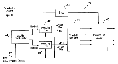
In accordance with the present invention, the signal 31 is applied to a
decision
device 40 illustrated in figure 4. The decision device 40 includes a
maximum/minimum
peak detector 41 which receives signal 31 and determines its maximum and
minimum
peak over a period of time P. Period P is programmable and selectable, and may
also
vary from application to application depending on parameters such as the bit
rate. In
figure 3, for regular operation the period P is shown to be equal to the
duration of five
symbols such that during period P,, the maximum and minimum measured would be
sl
and s4 respectively; during PZ - ss and s, respectively, during P3 - s, and s4
respectively,
during P4 - s2 and ss respectively, and so on.
After each period P, the maximum peak sample detected during that period is
fed
to a first averaging filter 42, while the minimum peak sample detected during
that period
is fed to a second averaging filter 43, with both filters ultimately operating
in parallel.
The averaging filters 43 may be finite impulse response filters (FIR) or
infinite impulse
response filters (IIR). If FIR filters are used for averaging, filters 42 and
43 will produce
an output signal representing the average maximum and average minimum
respectively at
the end of each period of time equivalent to nP based on n samples where n may
be in the
order of fifty (SO). Alternately, if IIR filters are used for averaging, the
filters provide a
dynamic average wherein the average of n samples is taken after each new
sample is
received. This allows the filters 42 and 43 to update the averages after every
period P.
In the preferred embodiment, filters 42 and 43 are infinite impulse response
(IIR)
filters 50 of the type shown in figure 5. The characteristic of IIR filter 50
is, that in its
averaging mode, it continuously provides at its output 52 the average of an
infinite
number of samples that it receives at its input 51. However, in filter SO the
input samples
are weighted such that the latest sample carries the most weight and the
weighting of each
sample by age may decrease exponentially. This is accomplished by the feedback
circuit
53 which applies a weighting factor Z-' and an amplification of a to the
output signal
CA 02296209 2000-O1-17
6
before feeding it back to summing circuit 55. The input sample on line 51 is
fed to an
amplifier 54 which applies an amplification factor of (1 -a) to the sample
before it is fed
to summing circuit 55. Thus once again the average at the output 52 is updated
with
every sample received at the input S 1. Though an infinite number of samples
theoretically enter into the determination of the average, in practice
depending on factors
a and Z-', and the precision used for computation, the latest fifty (50) or so
samples
actually affect the average.
Returning to figure 4, the average maximum signal Am~ and the average
minimum signal A~;~ are fed to a threshold combiner 44 where threshold levels
are
determined. One example of a threshold combiner 44 is illustrated in figure 6
as
combiner 60. Signals Am~ and A~,;n are applied to lines 61 and 62
respectively. Line 61
is connected to a first summing circuit 63 and a second summing circuit 64,
while line 62
is connected to the first summing circuit 63 and a third summing circuit 65.
The output
of the first summing circuit 63 is connected to a divide by 2 divider 66 to
provide an
output threshold signal To which is midway between A,~,~ and Amin at that
instant in time.
Threshold signal To may then be used to decode binary demodulated signals such
as the
one illustrated in figure 2. In an FSK demodulator, To represents the mid or
carrier
frequency of the FSK frequencies f~l and f_l.
To is also applied to summing circuits 64 and 65 which produce outputs equal
to
A",~ + To and Am;" + To respectively. These outputs are applied to divide by
(3 dividers 67
and 68 in order to produce two further threshold signals T+, and T_1
respectively.
Depending on the factor (3, T.,1 will be somewhere between To and Am~ and T_1
will be
somewhere between To and Am;". With factor (3 = 2, T+1 and T_, will be midway
between
To and Am~ and T., will be midway between To and A,n;o. Using the three
threshold levels
T+1, Ta and T.1, four level demodulated signals such as illustrated in figure
3 may be
efficiently decoded as will be described. However, in addition, the three
threshold levels
T+,, To and T_~ may further be used in the same manner as above to produce
further
CA 02296209 2000-O1-17
7
threshold levels T+~, and T_m if they are required to decode signals having
2'" levels where
m Z 3.
In order to decode the demodulated signal 31 received from the
demodulator/detector as illustrated in figure 4, the signal 31 is applied to a
delay circuit
45 which provides a small delay to the signal to make up for the inherent
delays produced
by signal processing in the averaging filters 42 and 43 as well as in the
threshold
combiner 44, but more importantly by the delay created in the peak detector 41
which
selects a maximum peak and a minimum peak during a period P. To compensate for
the
peak detector 41 delay, a delay of P would be required in the delay circuit
45. The
delayed signal 31 is then applied to decoder 46 where it is compared to the
threshold
levels T+,, To and T_1 to determine the actual output level of the signal 31.
One example of the decoder 46 is shown as decoder 70 in figure 7. Decoder 70
includes three comparators 71, 72 and 73. The delayed demodulated four level
signal 31
is applied to line 74 which is connected to the positive input of each of the
comparators
71, 72 and 73. T+, is applied to the negative input of comparator 71, To is
applied to the
negative input of comparator 72 and T-, is applied to the negative input of
comparator 73.
The outputs of comparators 71 and 72 are applied to the two inputs of a NAND
gate 75
and the outputs of comparators 72 and 73 are applied to the inputs of NAND
gate 76. In
addition, the output of comparator 71 is applied to one input of an OR-gate 77
with the
output of NAND-gate 76 applied to the other input of OR-gate 77. The resulting
outputs
on lines 78 and 79 from NAND-gate 75 and OR-gate 77 respectively represent the
signal
31 magnitude value for the four level FSK case.
In comparators 71, 72 and 73, when the input signal 3lis greater than the
threshold value applied to a comparator, the comparator generates a "1" and
when the
input signal is smaller than the threshold value applied to a comparator, the
comparator
generates a "0". Therefore, when signal 31 > T+,, the outputs of 71,72 and 73
are all "1";
CA 02296209 2000-O1-17
8
when signal 31 < T+I but > To, the output of 71 is "0" and the outputs of 72
and 73 are
" 1 "; when signal 31 < To but > T.+,, the outputs of 71 and 72 are "0" and
the output of 73
is "1 "; and when signal 31 < T_1 the outputs of 71, 72 and 73 are "0". As a
result, the
lines 78 and 79 will provide the following parallel binary code for the four
level signal:
line 78 line 79
signal 31 > T+1 0 1
T+, > signal 31 > To 0 0
To > signal 31 > T_, 1 0
signal 31 < T_1 1 1
Though the above coding was arbitrarily selected different coding may be
selected if
desired, then only the combinatorial logic following the comparators will
change. As the
number of levels in the signal 31 increases, the number of parallel binary
codes will also
increase. Thus a signal 31 with 2'" levels will result in m parallel binary
bits at the output
of decoder 46.
Referring to figure 4, the decision device 40 is activated when the peak
detector
41 receives a signal 47 from the received signal strength indicator (RSSI) in
the radio
receiver which normally indicates that the incoming signal is present. This
step signal 47
is also shown in figure 8. In order not to lose the data in the first part of
an incoming
signal, it is desirable to preload the averaging filters 50 using maximum and
minimum
sample values since the average maximum and average minimum values that can be
used
by the threshold combiner 44 are not initially available. As shown in figure
5, this is
achieved by including a bypass line 56, an amplifier 57 with an amplification
factor of
1/a and a switch 58 in each of the averaging filters 50 such that, when the
switch 58 is
positioned in the preload mode, a maximum/minimum sample value is applied to
the
summing circuit SS and out onto line 52 to the combiner 44 to generate
threshold values.
CA 02296209 2000-O1-17
9
As illustrated in figure 8, after the RSSI signal 47 goes high, the preload
mode is
initiated and the peak detector 41 is controlled to output maximum and minimum
sample
values at the end of each preload period P',where the preload period P' is
shorter than the
averaging period and is equal to the length of two symbols. In the averaging
mode, the
S peak detector 41 is controlled to output a maximum peak sample and a minimum
peak
sample at the end of each period P, where P is equal to the length of 5
symbols. It is
noted that initially signal 31 is somewhat erratic with substantial swings
between maxima
and minima, however the preloading of filters 50 is programmed to be repeated
for a
number of periods P' with the result that the maximum sample value and the
minimum
sample value being fed to the combiner 44 will result in the generation of
acceptable
threshold levels to decode the initial data in signal 31 after which time
switch 58 is
switched to the averaging mode such that the output of summing circuit 55 is
fed back to
the summing circuit 55 through feedback circuit 53. There is a smooth
transition between
the preload mode and the averaging mode, since the averaging circuit 50 uses
the last
preload sample value on which to apply the averaging process.
Though for convenience, the present invention was described using digital
circuitry, analog circuitry may also be used in its implementation.
While the invention has been described according to what is presently
considered
to be the most practical and preferred embodiments, it must be understood that
the
invention is not limited to the disclosed embodiments. Those ordinarily
skilled in the art
will understand that various modifications and equivalent structures and
functions may be
made without departing from the spirit and scope of the invention as defined
in the
claims. Therefore, the invention as defined in the claims must be accorded the
broadest
possible interpretation so as to encompass all such modifications and
equivalent
structures and functions.