Note: Descriptions are shown in the official language in which they were submitted.
CA 02296339 2000-O1-18
WO 99/05546 PCT/US98/12707
IMPROVED ANTI REFLECTIVE COMPOSTrE
The invention relates generally to improved composite structures exhibiting
optical properties and more specifically to such structures which exhibit anti-
reflective
properties utilized in display applications.
BACKGROUND OF THE INVENTION
For the last several years, anti-reflective composites have been used on an
ever
expanding basis for a myriad of purposes. Anti-reflective composites are most
commonly
used on windows, mirrors, and an assortment of display applications which
includes
television screens and computer monitor screens to minimize reflective
"glare."
The most common design for such composites is one having a quarter-wave
optical thickness at a particular wavelength. This design is capable of
reducing reflectance of
a surface to less than 1 ~ over the visible range.
A typical anti-reflective composite consists of a light transmissive substrate
and one or more transparent anti-reflective top layers. A transparent hard
coat layer is often
deposited between the substrate and the anti-reflective layers to give the
composite both
mechanical durability and physical strength. The materials used in each layer
and the
thicknesses of each layer are chosen so that a maximum amount of light is
transmitted
through the composite while a minimum amount of light is reflected by the
composite.
Numerous anti-reflective composite designs are known to date, most of which
are comprised of high and low refractive index materials in pairs. One of the
earliest patents
in this field, i.e., U.S. Patent No. 2,478,385, describes a three-layer
structure of
medium/high/low refractive index materials over a glass substrate.
CA 02296339 2000-O1-18
WO 99/05546 PCT/US98/12707
2
Another earlier patent dealing with anti-reflective coatings is U.S. Patent
No.
3,432,225, wherein is disclosed a method of combining a four-layer anti-
reflective coating
system using two different materials, i.e. ZrOi and MgF2. A basic problem with
this
approach is the inherent softness of MgF2, which limits the use of this
approach in many
applications.
Another mufti-layer anti-reflective coating is disclosed in U.S. Patent No.
3,565,509 wherein a three layer system is reduced to two using two materials
for production
simplicity.
The most common anti-reflective coating is a four layer structure. Such a
design can be made from two anti-reflective coating materials rather than from
three or four
different materials as indicated in some earlier patents. The thickness of
each layer is
optimized to obtain the best properties over a broad range of the spectrum.
Most anti-reflective composite designs utilize high index dielectric anti-
reflective layers as part of the construction. In applications where
electromagnetic shielding
and static discharge control are of primary concern, conductive high index
oxides such as
indium oxide or tin oxide are incorporated in the design structure. U.S.
Patent No.
4,422,721 covers the use of conductive coatings as part of the anti-reflective
design structure.
U.S. Patent No. 5,170,291 discloses a four-layer anti-reflective composite
where DC reactive sputtering has been suggested as a preferred method of
deposition. U.S.
Patent No. 5,5?9,162 discloses a mufti-layer anti-reflective composite
utilizing DC reactive
sputtering as a preferred method of deposition for temperature sensitive
substrates.
There are several problems with the anti-reflective composites presently
known. A first problem is that special processes are required to deposit anti-
reflective
coatings onto a polymeric substrate.
CA 02296339 2000-O1-18
WO 99105546 PCTIC1S98/I2707
3
A second problem is that most production techniques proposed for deposition
of various layers of anti-reflective composites are possible, but few are
practical. This is
particularly important since there is no documented method of depositing anti-
reflective
coatings in a continuous roll coating (web) system.
A third problem with presently known and-reflective composites is the general
lack of manufacturing efficiency and low deposition rates previously inherent
in the
manufacture of anti-reflective composites.
A fourth problem with presently known anti-reflective composites is the great
difficulty in being able to adhere anti-reflective coatings onto a polymeric
substrate,
especially a polymeric substrate which is covered with a hard coat.
Accordingly, there is a need for an improved anti-reflective composite which
overcomes these problems in the prior art.
The present invention solves these problems. The present invention is an anti-
reflective composite having very high visible light transmission and
negligible visible
reflectance over 400nm - 800nm wavelengths. Such coatings may be suitable for
any
surfaces requiring low light reflectance and requiring electrical and magnetic
shielding. The
proposed anti-reflective composites have utilization in a variety of display
applications.
In one embodiment, the invention is an anti-reflective composite comprising:
(a) a light transmissive substrate; (b) a hard coat deposited onto the
substrate; (c) a first
transparent oxide layer deposited onto the hard coat; and (d) a second
transparent oxide layer
deposited onto the first transparent oxide layer. Preferably, the transparent
oxide layers are
deposited by pulsed magnetron sputtering comprising either medium frequency AC
sputtering
or symmetric/asymmetric bi-polar DC sputtering.
CA 02296339 2002-03-15
4
In another preferred embodiment of the invention, a
thin carbon layer, having an average thickness between about
2~ and about 1OOI~ is deposited between the hard coat and the
substrate. In another preferred embodiment of the invention,
a thin carbon layer, having an average thickness of between
about 2~ and about 100 is deposited between the outermost
transparent oxide layer and the low surface energy layer.
In more sophisticated embodiments of the invention,
the composite comprises at least one pair of oxide layers
deposited on top of the hard coat. Each pair of oxide layers
comprises (i) a first transparent oxide layer deposited onto
the hard coat, the first transparent oxide layer having a
refractive index between about 1.65 and about 2.65 and having
an average thickness between about 100 and about 3200; and
(ii) a second transparent oxide layer deposited onto the first
transparent oxide layer, the second transparent oxide layer
having a refractive index between about 1.2 and abut 1.85 and
having an average thickness between about 100 and about 3200.
In a preferred embodiment of the composite described
immediately above having at least one pair of oxide layers, one
of the transparent oxide layers is a tertiary oxide layer.
In another preferred embodiment of the composite
having at least one pair of oxide layers, a layer of aluminum
oxide or zirconium oxide having a thickness between about 400
and about 1000 is deposited between the hard coat and the
pair of oxide layers. Other oxides possessing refractive
indices of about 1.50 to about 2.20 can replace the above
mentioned articles.
In still another preferred embodiment of the
composite having at least one pair of oxide layers, the second
transparent oxide layer in the outermost pair has an index of
refraction between about 1.2 and about 1.85 and has a low
surface energy of 40 dynes/cm or less.
CA 02296339 2000-O1-18
WO 99/05546 PCT/US98/12707
In another preferred embodiment, the low surface energy layer is a vacuum
deposited organic/inorganic mixture.
The transparent layers may be deposited by vacuum or non-vacuum processes
5 or by a combination of both.
The hard coat layer may be an "ordinary" organic hard coat layer having an
index of refraction between about 1.4 and about 2 and having an average
thickness between
about 0.5 and about 10 microns, preferably deposited by a wet chemistry
process. The hard
coat layer can also be either an inorganic material or an organic/inorganic
material having an
index of refraction between about 1.5 and about 2 and having an average
thickness between
about 0.5 and 10 microns, preferably deposited by a vacuum process.
DIGS
These features, aspects and advantages of the present invention will become
better understood with regard to the following description, appended claims
and
accompanying figures where:
Figure 1A is a diagrammatic representation of an anti-reflective composite
having features of the invention;
Figure 1B is a graph showing the anti-reflectance properties of an anti-
reflective composite such as illustrated in Figure 1 A;
Figure 2A is a diagrammatic representation of a second anti-reflective
composite having features of the invention;
Figure 28 is a graph showing the anti-reflective properties of an anti-
reflective
composite such as illustrated in Figure 2A;
CA 02296339 2000-O1-18
WO 99/05546 PCT/US98/12707
6
Figure 3A is a diagrammatic representation of a third anti-reflective
composite
having features of the invention;
Figure 3B is a graph showing the anti-reflective properties of an anti-
reflective
composite such as illustrated in Figure 3A;
Figure 4A is a diagrammatic representation of a fourth anti-reflective
composite having features of the invention;
Figure 4B is a graph showing the anti-reflective properties of another anti-
reflective composite, such as illustrated in Figure 4A; and
Figure 5 is a diagram of a sputter coating machine useable in the invention.
The following discussion describes in detail one embodiment of the invention
and several variations of that embodiment. This discussion should not be
construed,
however, as limiting the invention to those particular embodiments.
Practitioners skilled in
the art will recognize numerous other embodiments as well.
The invention is an improved anti-reflective composite. In all embodiments of
the invention, the composite comprises a substrate and one or more anti-
reflective layers
deposited onto the substrate.
The substrate is light transmissive. The substrate can be a rigid material,
such
as glass or rigid polycarbonate. Preferably, the substrate is a flexible
material, capable of
being provided in a roll format, such as flexible polymeric material.
Typically, such
materials are flexible polycarbonate, polyethylene terephthalate ("PET") and
other flexible
polymeric materials having excellent optical and roll conformation properties.
CA 02296339 2002-03-15
7
Where the substrate is a flexible material, a
transparent hard coat is commonly applied to give the substrate
both additional physical strength as well as mechanical durability.
The hard coat can also possess certain optical properties which can
be used in structuring the overall anti-reflective composite.
In one embodiment of the invention, the hard coat is a
"massive hard coat" layer having a thickness between about 0.5 and
about 10 microns, and having a refractive index between about 1.2
and about 2. Typically, such a massive hard coat layer is chosen
to be vacuum compatible for reduced degassing properties when being
vacuum deposited. Suitable materials used to produce such massive
hard coat layers are (i) polyurethanes, (ii) polymerizable long
chain acrylics and methoxsiloxanes, and (iii) silicates, densely
cross-linked acrylic polymers, solvent-cast epoxies and
combinations of the above.
A preferred massive hard coat useful in the invention is
an inorganic hard coat having an index of refraction between about
1.5 and about 2. Such a hard coat can be comprises of A1203, and/or
Si02. Alternatively, a massive hard coat can also consist of an
organic/inorganic material having an index of refraction between
about 1.5 and about 2 deposited preferably by a vacuum deposition
process.
One or more anti-reflective layers are deposited onto
the hard coat. Such anti-reflective layers are chosen to have a
thickness and refractive index so that the anti-reflective layers,
in combination with the substrate and the hard coat, providing a
composite exhibiting anti-reflective properties.
Preferably, a thin layer of carbon is deposited between
the hard coat layer and the anti-reflective layers. The carbon
layer has a thickness between about 2~ and about 100. The carbon
layer serves as an adhesion promoting layer between the hard coat
and the anti-reflective layers, particularly where the anti
reflective layers are deposited by sputtering. The carbon layer
has also been found to minimize surface out gassing from the hard
coated substrate. The nature of the carbon layer and methods for
depositing it are fully described in U.S. Patent Nos. 4,802,967,
4,865,711 and 4,913,762 (all issued to Wilfred Kittler).
CA 02296339 2002-03-15
8
Without such_a carbon layer, other techniques such
as chemical treatment, corona discharge, glow discharge or the
deposition of a sub-oxide (primer) layer are used in an attempt
to provide adequate adhesion between the hard coated substrate
and the anti-reflective layers. All of these prior art
attempts, however, provide insufficient adhesion, are unduly
expensive or have other associated production problems with
them.
In the invention, the thin layer of carbon is
deposited on top of the hard coat, preferably by sputtering.
The carbon layer is especially useful in promoting
the adhesion of the hard coat to materials having a low surface
energy or a critical surface tension.
The carbon layer has further been found to minimize
the outgassing of hard coats, one of the major problems in
working with hard coats. By minimizing outgassing, composites
of the invention using the thin carbon layer are considerably
more stable and uniform during the deposition of the anti
reflective coating.
The carbon layer can also be used as an adhesion
promoting layer interposed between the substrate and the hard
coat layer and between the low surface energy layer and the
outermost transparent oxide layer. For example, an anti-
reflective composite can be provided which comprises a flexible
(substrate normally PET), a massive hard coat layer disposed
onto the flexible substrate, and oxide layers disposed onto the
hard coat layer, wherein a thin layer of carbon is interposed
between the substrate and the hard coat, between the hard coat
and oxide layers and/or between the oxides and the low surface
energy layer of less than 40 dynes/cm.
The anti-reflective layers can be deposited by vacuum
deposition techniques well-known in the art. Examples are
evaporation, sputtering, PECVD, etc. In a typical embodiment,
the anti-reflective layers are deposited by single or multiple
CA 02296339 2002-03-15
9
cathode sputtering processes.
In one embodiment of the invention, the anti-reflective
layers are deposited by a dual cathode sputtering method. A dual
cathode sputtering method employs a mid-frequency AC sine wave
pulse power supply. Dual cathode systems use two magnetron
cathodes, disposed side by side. Dual cathode systems minimize
problems with traditional DC magnetron sputtering, including arc
control and inherent anode problems.
Inherent anode problems arise in reactive DC sputtering
because the process chamber, the anode, as well as the greater part
of the target, become covered by randomly grown insulating layers.
The coverage of the anode and shielding with the insulating layer
results in varying and difficult process conditions. Many "micro-
arcs" are created during the sputtering of oxides causing defects
in the deposited layer. To avoid this arcing, some people have
used RF sputtering techniques, but the industrial applicability of
RF sputtering is very restricted due to its low deposition rates
and difficulty in matching network requirements.
In dual cathode sputtering, two magnetron sources are
connected to a bi-polar pulse generator so that each cathode
alternatively acts as the cathode and an anode of a magnetron
discharge. In contrast to DC sputtering, the power is fed into the
reaction discharge in a pulsed mode with a frequency in the range
of 20-100 khz, which hinders the discharging of insulating regions
and prevents the target from arcing. Dual cathode sputtering
provides for the creative sputter deposition of coating materials
which otherwise could not be produced on a large scale using DC
sputtering technology.
Dual cathode magnetron sputtering methods offer the
following advantages over DC sputtering methods of the prior art
and other prior art coating technologies, such as DC and RF
methods:
(1) Deposition rates are higher than in equivalent DC
and RF-type sputtering methods:
(2) Increased process stability over long operating
periods;
CA 02296339 2000-O1-18
WO 99/05546 PCT/US98/12707
(3) Minimized layer imperfections due to arcing; and
(4) Cross-web uniformity of less than 2 Y can be readily achieved.
Dual cathode sputtering methods are preferred, especially for the production
of
5 both conductive and non-conductive anti-reflective composites comprising
multiple anti-
reflective coating layers.
Dual cathode sputtering is especially preferred where the anti-reflective
layers
are highly insulating (e.g., dielectric) materials. Arcing in reactive DC
sputtering
10 depositions of highly insulating materials is initiated by the electrical
breakdown processes of
the insulating layer on the magnetron cathode. This is because the deposition
equipment
includes a looping magnetic field which restricts the sputter erosion of the
target to the "race
track" area. In this area, the sputter rate is higher than the growth caused
by back-sputtering.
However, in a location further away from the race track growth rate exceeds
target erosion
IS and consequently these parts of the target will be covered with an
insulating layer. This
coverage will cause arcing of various types. Because of these arcs, there are
defects in the
coating layer and it is also very difficult to control the process.
The above-mentioned problem regarding DC sputtering can be resolved in
principal by using RF techniques. However, RF sputtering does not provide high
deposition
rates. RF sputtering also generally entails high thermal substrate loads and
high particle
energy. Thus, RF sputtering is unsuitable for large area substrate coatings
and for thermally
sensitive flexible film substrates.
In another embodiment of the invention, the method of depositing the anti-
reflective layers is symmetric/asymmetric bi-polar pulsed DC sputtering.
Asymmetric bi-
polar pulsed DC sputtering is preferred for single cathode sputtering because
it minimizes
problems with target poisoning associated with reactive DC sputtering methods.
In reactive
DC sputtering methods, there is a tendency to build up insulating layers on
the target surface
("target poisoning"). When an insulator is deposited on the surface of the
target, a capacitor
is formed. The target acts as one conductor, the plasma as the other conductor
and the
CA 02296339 2000-O1-18
WO 99/05546 PCT/US98/12707
11
insulating film forms the dielectric of the capacitor. Problems then occur
because DC
currents cannot flow through a capacitor. The first problem is that, without
current flow,
there can be no sputtering from this area of the target. Current flow is ion
current, and
therefore, if no argon ions strike the area, then no target atoms can be
freed, and therefore no
sputtering can occur. The second problem is that the capacitor formed may not
have enough
dielectricity to withstand the capability to charge all the way up to the
applied voltage. If
not, the breakdown of the insulation will cause a sudden release of charge
carriers, forcing
the local current density to increase into the area discharge region, which
results in arcing.
This arcing causes defects in the insulator films.
Asymmetric bi-polar pulsed DC sputtering, on the other hand, allow the set up
of conditions which cause insulators on the target to be sputtered first with
a higher sputter
yield than the base material. This "preferential sputtering" effectively
eliminates target
poisoning. Preferential sputtering is accomplished by adding a reverse voltage
bias pulse to
the normal DC waveform. If the typical sputtering runs at -400 volts, the
polarity is rapidly
reversed to about + 100 volts, causing the capacitor to be charged to opposite
(-100 volts) on
the surface exposed to the plasma. No sooner the reverse pulse ends and the
voltage returns
to sputter mode (-400 volts), the plasma side of the capacitor is charged to -
100 volts. When
the target reaches -100 volts, the effective voltage on the plasma is -500
volts. Thus, the
argon ions are drawn by electrostatic attraction to the insulators and strike
with extra energy
(-500 volts), which sputters the insulators off the target first, eliminating
target poisoning and
arcing.
Asymmetric bi-polar pulsed DC method depends on pulse frequency because
the pulses must occur frequently enough to prevent charge build-up on the
capacitors from
exceeding the breakdown voltage. Typical process frequencies are between about
80 khz and
about 150 khz. The reverse bias cannot be too high, as it will make a change
from charging
the capacitors to sputtering the shields and chamber walls. Typical voltages
use are between
about +75 to about + 150 volts.
Dual cathode symmetric/asymmetric bi-polar pulsed DC method uses a bi-
CA 02296339 2000-O1-18
WO 99/05546 PCT/US98/12707
12
polar pulse power source with a periodic square-wave pulse chain. This offers
independent
control of positive and negative pulse times for the output voltage, and
delivers maximum
performance. By virtue of the free adjustability and the selectivity of the bi-
polar pulsed DC
do+, dc-, unipolar+ and unipolar- control functions are possible. This allows
a plasma
treatment of materials, such as conductors, semi-conductors and non-
conductors.
In general, for insulating layers one can use pulse DG sputtering for
increasing
the deposition rate, eliminating arcing and obtaining high quality film at low
temperatures.
Unlike sinusoidal (AC) sputtering, the bi-polar pulsed DC (square wave form)
gives
independent control of "on and off times to adjust the balance between plasma
density and
avoidance of arcing. The positive and negative pulse widths are adjustable
over a
considerable range from a few microseconds up to about one half second, and
variable off
times are available between the pulses. Frequency can be varied.
Dual cathode sputtering methods utilizing medium frequency AC pulsed power
supply and symmetric/asymmetric bi-polar DC sputtering techniques are easily
adaptable to
wide area roll coating machines capable of depositing the anti-reflective
layers over a
continuous length of a substrate material.
In preferred embodiments of the invention, the anti-reflective layers are
provided by at least one pair of oxide layers deposited on top of the hard
coat. Each pair of
oxide layers comprises (i) a first transparent oxide layer deposited onto the
hard coat, the
first transparent oxide layer having a refractive index between about 1.65 and
about 2.65 and
having an average thickness between about 100 and about 3200 ~; and (ii) a
second
transparent oxide layer deposited onto the first transparent oxide layer, the
second transparent
oxide layer having a refractive index between about 1.2 and about 1.85 and
having an
average thickness between about 100 and about 3200 A. Preferably, the first
transparent
oxide layer is an electrically conductive coating.
CA 02296339 2002-03-15
13
In one most preferred embodiment, one of the transparent
oxide layers is a tertiary alloy, such as InZNSnOx InZnGaOx and
InZnMgOX .
In another highly preferred embodiment, a layer of
aluminum oxide or zirconium oxide having a thickness of about 400
and about 1000 is interposed between the hard coat and the pair
of oxide layers. This interposed layer is chosen to have an index
of refraction between about 1.50 and about 2.20.
In all of the embodiments of the invention, a low
surface energy layer commonly known as an "anti-smudge" layer can
be disposed on top of the anti-reflective layers. Typically, such
an anti-smudge layer has a low surface energy of about 40 dynes/cm
or less. In unique embodiments of the invention, at least one pair
of the oxide layers, the second transparent oxide layer in the
outermost pair, has an index of refraction between about 1.2 and
about 1.85, and has a low surface energy of 40 dynes/cm or less.
In a preferred embodiment of the invention, by
interposing a layer of aluminum oxide or zirconium oxide between a
carbon coated hard coat and a pair of transparent oxide layers, a
composite having two anti-reflective layers can be made to perform
as well as prior art composites having four or more anti-reflective
layers.
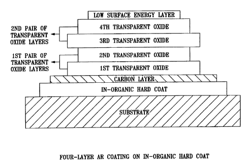
Figures 1A and 4A illustrate two different anti-
reflective composites comprising four anti-reflective layers
disposed on a hard coat layer. Figure 2A illustrates an anti-
reflective composite having two anti-reflective layers, and Figure
3A illustrates~an anti-reflective composite having three anti-
reflective layers.
Figure 1B illustrates the anti-reflective properties of
an anti-reflective composite such as illustrated in Figure 1A. The
substrate is PET and has a refractive index of 1.65. The hard coat
is an inorganic A1203 material, vapor deposited onto the substrate.
The hard coat has a refractive index of 1.70 and has an average
thickness of 4 microns. The carbon layer has an average thickness
of 5~. The carbon layer is deposited by vacuum deposition. The
first transparent oxide layer is Si02, having a refractive index of
1.46. The second transparent oxide layer is A1203, having a
CA 02296339 2002-03-15
14
refractive index of 1.70. The third transparent oxide layer is
ITO, having a refractive index of 2.0, and the fourth refractive
oxide layer is Si02, having a refractive index of 1.46. Each of
the transparent oxide layers is deposited by pulsed magnetron
sputtering comprises of medium frequency AC sine wave sputtering
and symmetric/asymmetric bipolar pulsed DC sputtering. The low
surface energy layer is deposited on the top of the fourth
transparent oxide layer. The low surface energy layer is a
fluoropolymer material having a refractive index of 1.38, and an
average thickness of 20~. The low surface energy layer has a
surface energy of less than about 40 dynes/cm.
Figure 2B illustrates the anti-reflective properties of
two anti-reflective composites having a two-layer design, such as
illustrated in Figure 2A. In both designs, the substrate material
is PET and has a refractive index of 1.65. The hard coat is a W
cured acrylic hard coat applied onto the substrate. The hard coat
has a refractive index of 1.63 and has an average thickness of 6
microns. The carbon layer has an average thickness of 5~. The
carbon layer is deposited by vacuum deposition. The first
transparent oxide layer is ITO having a refractive index of 2Ø
The second transparent .oxide layer is Si02, having a refractive
index of 1.46. Each of the transparent oxide layers is deposited
by pulse magnetron sputtering comprised of medium frequency AC sine
wave sputtering and symmetric/asymmetric bipolar pulsed DC
sputtering. The low surface energy layer is deposited on the top of
the second transparent oxide layer. The low surface energy layer
is a fluoropolymer material, having a refractive index of 1.38, and
an average thickness of 20~. The low surface energy layer has a
surface energy of less than about 40 dynes/cm.
The only difference between the two anti-reflective
composites whose anti-reflective properties are illustrated in
Figure 2A is the hard coat refractive indices and the coating
thicknesses.
Figure 3B illustrates the anti-reflective properties of
two anti-reflective composites, one having a three-layer design,
such as illustrated in Figure 3A, and one having a four-layer
design, such as illustrated in Figure 1A. In the three-layer
design, the substrate material is PET and has a refractive index of
CA 02296339 2002-03-15
1.65. The hard coat is a W cured acrylic hard coat applied onto
the substrate. The hard coat has a refractive index of 1.50, and
has an average thickness of 6 microns. The carbon layer has an
average thickness of 5I~ and is deposited by vacuum deposition. The
first transparent oxide layer is A1203, having a refractive index
of 1.70. The second transparent oxide layer is ITO, having a
refractive index of 2Ø The third transparent oxide layer is
Si02, having a refractive index of 1.46. The low surface energy
10 layer is deposited on the top of the third transparent oxide layer.
The low surface energy layer is a fluoropolymer material, having a
refractive index of 1.38, and an average thickness of 20~. The low
surface energy layer has a surface energy of less than about 40
dynes/cm.
The four-layer design whose reflective properties are
illustrated in Figure 3B has a PET substrate with a refractive
index of 1.65. The hard coat is a UV cured acrylic hard coat
material, applied onto the substrate. The hard coat has a
refractive index of 1.50, and has an average thickness of 6
microns. The carbon layer has an average thickness of 5~. The
carbon layer is deposited by vacuum deposition. The first
transparent oxide layer is ITO, having a refractive index of 2Ø
The second transparent oxide layer is Si02, having a refractive
index of 1.46. The third transparent oxide layer is ITO, having a
refractive index of 2.0, and the fourth transparent oxide layer is
Si02, having a refractive index of 1.46. Each of the transparent
oxide layers is deposited by pulsed magnetron sputtering comprises
of medium frequency AC sine wave sputtering and
symmetric/asymmetric bipolar pulsed DC sputtering. The low surface
energy layer is a fluoropolymer material, having a refractive index
of 1.38, and an average thickness of 20~. The low surface energy
layer has a surface energy of less than about 40 dynes/cm.
Figure 4B illustrates the anti-reflective properties of
an anti-reflective composite, such as illustrated in Figure 4A. In
this embodiment, the substrate is PET and has an index of 1.65.
The hard coat is a UV cured acrylic hard coat material, applied
onto the substrate. The hard coat has a refractive index of 1.50,
and has an average thickness of 6 microns. The carbon layer has an
average thickness of 5~ and is deposited by vapor deposition. The
CA 02296339 2002-03-15
16
first transparent oxide layer is ITO, having a refractive index of
2Ø The second transparent oxide layer is Si02, having a
refractive index of 1.46. The third transparent oxide layer is
ITO, having a refractive index of 2.0, and the fourth transparent
oxide layer is Si02, having a refractive index of 1.46. Each of the
transparent oxide layers is deposited by pulsed magneton sputtering
comprised of medium frequency AC sine wave and asymmetric bipolar
pulsed DC sputtering. The low surface energy layer is a
fluoropolymer material, having a refractive index of 1.38, and an
average thickness of 20~. The low surface energy layer is
deposited by wet chemistry and sputtering. The low surface energy
layer has a surface energy of less than about 40 dynes/cm.
The following describes the preparation of an anti-
reflective composite having features of the invention. This
example is provided for illustrative purposes only, and is not
meant to limit the scope of the invention.
EXAMPLE
A four-layer anti-reflective composite is produced in a
laboratory scale research and development roll to roll sputtering
coater, such as illustrated in Figure 5. The cathode size is 15"
x 4.5" and the drum size is 16". Figure 5 shows a schematic
diagram of a laboratory scale R & D sputtering coater.
Description of Vacuum Coating Process:
Substrate: Flexible roll of 175 microns hard coated PET.
Refractive index of PET is 1.65 thickness of
the hard coat is 6 microns and refractive
index is 1.50
Pass 1: Glow discharge (plasma cleaning) process
conditions:
Gas: argon: oxygen 50:50
Power: 50 watts
Voltage: 900 volts
Current: 0.06 amps
Speed: 2.5 ft/min.
CA 02296339 2000-O1-18
WO 99105546 PCT/US98112707
17
Pass 2:
Carbon layer process conditions:
Target: Carbon (99.9999
0
Gas: Argon 100 sccm
Power: 1.5 kilowatts
Voltage: 562 volts
Current: 2.68 amps
Speed: 24 ft./min.
Total Pressure: 2.56 microns
Deposition Technique: DC sputtering
Pass 3:
First transparent oxide layer process conditions:
Target: In/Sn 90/ 10
Gas: Argon: 100 sccm Oxygen: 34 sccm
Power: 2.5 kw
Voltage: 369 volts
Current: 6.8 amps
Speed: 4.5 ft.lmin.
Total Pressure: 2.54 microns
Deposition Technique: Asymmetric bipolar pulsed DC
sputtering
Pass 4:
Second transparent oxide layer process conditions:
Target: Silicon (Boron doped)
Gas: Argon: 68 scan Oxygen: 25 sccm
Power: 2.5 kw
Voltage: 396 volts
Current: 6.3 amps
Speed: 2.6 ft./min.
Total Pressure: 2.0 microns
Deposition Technique: Asymmetric bipolar pulsed DC
sputtering
CA 02296339 2000-O1-18
WO 99/05546 PCT/US98/12707
18
Third transparent oxide layer process conditions:
Target: 90:10 Indium/Tin.
Gas: Argon: 100 sccm Oxygen: 34 sccm
Power: 2.5 kw
Voltage: 369 volts
Current: 6.8 amps
Speed: 1.63 ft./min.
Total Pressure: 2.54 microns
Deposition Technique: Asymmetric bipolar pulsed DC sputtering
Pass 6:
Fourth transparent oxide layer process conditions:
Target: Silicon (Boron doped)
Gas: Argon: b8 sccm Oxygen: 25 sccm
Power: 2.5 kw
Voltage: 396 volts
Current: 6.3 amps
Speed: 0.68 ft./min.
Total Pressure: 2.0 microns
Deposition Technique: Asymmetric bipolar pulsed DC
sputtering
After the vacuum deposition of the hardcoated PET, a very thin low surface
energy layer (fluoropolymer) was deposited onto the sample by wet chemistry.
Properties of the above anti-reflective composite:
Total transmittance: > 92 36
Reflection average between 450 and 650nm: 0.45 %
Adhesion test (cmss cut 100 squares 1.5 mm, snap 5 times): pass
Hardness test (ASTM D 3363): Pass (3H pencil)
CA 02296339 2002-03-15
19
Steel wool abrasion (#0000 Steel wool 60 strokes 200 gms
weight): pass (no visible deterioration)
Humidity test (50°c, 95~ RH for 48 hours): pass
reflectance, adhesion and ethanol abrasion
Electrical conductivity: less than 250 ohms/sq.
Low surface energy layer (anti-smudge): less than 40
dynes/cm.
Samples produced had excellent anti-reflective
properties, extremely durable, with very low reflection and good
transmission. These samples, when applied to display screen
(television or computer monitor) drastically enhanced the
brightness by reducing light glare on the screen.
Having thus described the invention, it should be
apparent that numerous structural modification and adaptations may
be resorted to without departing from the scope and fair meaning of
the instant invention.