Note: Descriptions are shown in the official language in which they were submitted.
CA 02296519 2000-O1-12
WO 99/04452 PCT/KR97/00270
- 1 -
DUAL BAND ANTENNA
BACKGROUND OF THE INVENTION
1. Field of the Invention
The present invention relates to antennas, and more
particularly, to a dual band antenna for mobile
communications.
2. Description of the Related Art
With the rapid progress of mobile communications,
the capacity of existing systems is becoming saturated,
and thus, new systems are being developed at new
frequencies to enhance capacity. Accordingly, the
interrelationship between existing arid new systems must
be taken into consideration in the design of mobile
communications equipment. For mobile communications
antennas, major design concerns are power efficiency and
effective use of frequency.
In practice, it is desirable in the Republic of
Korea (South Korea) to interlink the existing CDMA (Code
Division Multiple Access) system with the new PCS
(Personal Communication System) system, in the U.S.A. to
interlink the existing AMPS (Advanced Mobile Phone
Service) system with the PCS system, and in Europe to
interlink the existing GSM (Groupe Speciale Mobile)
system with the DCS (Digital Communication System) 1800
system. Generally, a "dual band system" is a system that
CA 02296519 2000-O1-12
WO 99/04452 PCT/KR97/00270
- 2 -
allows for communications within two different systems at
different frequency bands, such as in above examples. It
is desirable to manufacture communications equipment
capable of operating within dual band systems.
Heretofore, each radio telephone terminal in the
dual band systems are provided with two separate
miniature antennas for two different bands, which results
in increased production cost. Also, the use of two
antennas for this purpose is an obstacle to the
miniaturization of the radio telephone terminal, and
results in an inconvenience to the user. For these
reasons, it is required to develop a dual band antenna
capable of being used for both bands.
U.S. Patent No. 4,509,056 discloses a
mufti-frequency antenna employing a tuned sleeve choke.
Referring to FIG. 1, an antenna of the type disclosed in
that patent is shown. This antenna operates effectively
in a system in which the frequency ratio between
operating frequencies is 1.25 or higher. The internal
conductor 10 connected to coaxial feed line 2 and the
sleeve choke 12i act as a radiating :element. The feed
point of sleeve choke 12i is short-circuited and the
other end thereof is open. The lengths of conductor 10
and sleeve choke 12i are designed so as to achieve
maximum efficiency at a desired frequency.
The choke 12i is partially filled with dielectric
material 16i that is dimensioned so that the choke forms
a quarter wavelength transmission line and prevents
coupling between the shell 14i and the extension 10 at
the open end of the choke at the highest frequency. At
some lower frequency of operation, the choke 12i becomes
ineffective as an isolation element and the entire length
P of the structure from the ground plane to the end of
the conductor, becomes a monopole antenna at the lower
CA 02296519 2000-O1-12
WO 99/04452 PCT/KR97/00270
- 3 -
resonant frequency.
The coupling between conductor 10 and sleeve choke
12i occurs at the open end of sleeve choke 12i. That is,
when the length 1 = 4 , the choke acts as a high
impedance, whereby the coupling between conductor 10 and
sleeve choke 12i is minimal. When 4 ~1, the choke
acts as a low impedance, whereby the coupling between
conductor 10 and choke 12i is higher. The electrical
length of choke 12i can be adjusted by varying the
dielectric constant of dielectric material 16i.
The construction consisting of internal and external
conductors 10, 14i is regarded as coaxial transmission
line, and its characteristic impedance is expressed as
foflows
Z~ = 59 . 95/~ In (D/d) ( 1)
where eI is dielectric constant, D is the diameter
of the external conductor, and d is the diameter of the
internal conductor. The input impedance between internal
and external conductors 10, 14i is denoted by the
following equation:
Zin = Z ZL+~Z~tanhy'1 ( 2 )
Z~+ j ZLtanhy'1
where y = a+j~3 , a is attenuation factor, b is
propagation constant, I is length of transmission line,
and zL is load impedance.
In the antenna of FIG. 1, the ground plate 20 and
external conductor 14i are structurally adjacent to each
other, thereby causing parasitic capacitance which
degrades the antenna efficiency. To improve the antenna
efficiency, the parasitic capacitance can be decreased.
Accordingly, in the construction of FIG. 1, the diameter
of external conductor 14i must be reduced for this
CA 02296519 2000-O1-12
WO 99/04452 PCT/KR97/00270
- 4 -
purpose, which is ultimately the same as the reduction of
characteristic impedance of choke 12i according to the
above equation (1). That is, such reduction in the
characteristic impedance of choke 12i gives rise to a
change in the amount of coupling, resulting in a
degradation of the antenna's performance.
Thus, to minimally affect the amount of coupling and
to keep the characteristic impedance of choke 12i
essentially the same as it was previously (i.e., before
the diameter of conductor 14i changed), the diameter of
internal conductor 10 must be reduced. This results in
a reduction in the antenna's bandwidth. Therefore, when
the antenna is manufactured in such a manner, the same
cannot satisfactorily cover the frequency bandwidth
required for the system.
Further, since the dielectric material is employed
to adjust the quantity of coupling, the dielectric
constant and the dimension of the dielectric material
must be accurately selected for proper coupling.
SUMMARY OF THE INVENTION
It is an object of the present invention to provide a
dual band antenna with improved performance and
bandwidth, by minimizing parasitic capacitance between
ground and an external conductor thereof.
It is another object of the present invention to provide
a dual band antenna which has a simple and compact
structure and high performance.
It is still another object of the present invention to
provide a dual band antenna which is inexpensive and
convenient to use.
In an exemplary embodiment of the present invention, a
CA 02296519 2002-08-22
75998-55
- 5 -
dual band antenna includes an inductor, first and second
rod-like radiating elements connected to opposite ends of
the inductor, and dielectric material surrounding both the
inductor and the joining portions of the first and second
radiating elements on the respective ends of the inductor.
A conductive support housing, e.g., a cylindrical metal
housing, surrounds the dielectric and supports the inductor
and the joining portions of the first and second radiating
elements. The housing and dielectric create a capacitance,
such that an LC resonant circuit is formed in conjunction
with the inductor. The LC circuit is designed so that only
one radiating element radiates at the higher band of the
dual operating band, whereas both radiating elements radiate
at the lower band.
A broad aspect of the invention provides a dual
band antenna comprising an inductor, first and second rod-
shaped radiating elements connected to opposite ends of said
inductor; dielectric material surrounding: said inductor, a
portion of said first radiating element connected to one end
of said inductor, and a portion of said second radiating
element connected to the other end of said inductor; and a
conductive housing surrounding said dielectric material and
supporting said inductor together with joined portions of
said first and second radiating elements, thereby forming
capacitance together with said dielectric material.
BRIEF DESCRIPTION OF THE DRAWINGS
FIG. 1 is a sectional view of a monopole antenna
operating at dual frequencies according to a conventional
embodiment of a multi-frequency antenna employing tuned
sleeve chokes;
CA 02296519 2002-08-22
75998-55
- 5a -
FIG. 2 is a sectional view illustrating the
construction of a dual band antenna according to an
embodiment of the present invention;
FIG. 3 is a circuit diagram illustrating the
equivalent circuit of the antenna shown in FIGS. 1 and 2;
FIG. 4 is a graph illustrating standing wave ratio
(SWR) of an experimental dual band antenna in accordance
with a embodiment of the invention; and
FIG. 5 is a Smith chart illustrating measured
results for a dual band antenna in accordance with an
embodiment of the invention.
CA 02296519 2000-O1-12
WO 99/04452 PCT/KR97/00270
- 6 -
DETAILED DESCRIPTION OF THE PREFERRED EMBODIMENT
The present invention will now be described more
specifically with reference to the drawings attached only
by way of example. It is to be noted that like reference
numerals and characters used in the accompanying drawings
refer to like constituent elements.
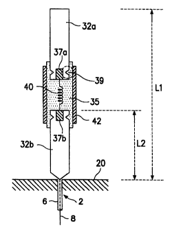
Referring to FIG. 2, a cross section of an exemplary
dual band antenna in accordance with the invention is
shown. The antenna includes an inductor 40, first and
second rod-shaped radiating elements 32a, 32b, each
connected to the respective ends of inductor 40, with
dielectric material 35 surrounding the entire inductor
and the joined portions of first and second radiating
elements 32a, 32b on the respective ends connected to the
inductor 40. A conductive cylindrical support housing
42, e.g., a cylindrical metal housing, fixes inductor 40
in place and supports the same, as well as supporting the
related joint portions of first and second radiating
elements 32a, 32b. Support housing 42 and dielectric 35
together form a capacitive structure, whereby an LC
resonant circuit is created in conjunction with inductor
40.
First and second radiating elements 32a, 32b are each
provided with grooves 39 which are filled with dielectric
material 35. A bearing structure of the radiating
elements 32a, 32b is thereby formed, since a uniform
horizontal force is applied from the cylindrical metal
housing 42 to the dielectric~inaterial 35. The other end
of the second radiating element 32b is connected to
internal conductor 8 of coaxial feed line 2. The outer
conductor 6 of coaxial line 2 is connected to ground
plate 20. The reference numerals 37a and 37b indicate
the joint portions between inductor 40 and first and
CA 02296519 2000-O1-12
WO 99/04452 PCT/KR97/00270
second radiating elements 32a, 32b. For example, these
joints can be solder connections.
FIG. 3 shows a circuit diagram illustrating a lumped
element equivalent circuit for the antenna of FIG. 1 or
2. In the equivalent circuit, the coupling between first
and second radiating elements 32a, 32b is denoted by
capacity C and inductor L.
Referring collectively to FIGS. 2 and 3, in the
embodiment of the present invention, the amount of
coupling between the first and second radiating elements
32a, 32b can be controlled via inductor 40, dielectric
material 35, and cylindrical metal housing 42. The
overall length of the antenna is determined on the basis
of first and second radiating elements 32a, 32b, inductor
40, and the operating frequency band. More specifically,
the overall antenna length L1 is determined as a function
of wavelength in the lower operating frequency band. In
the lower frequency band, both the first and second
radiating elements 32a, 32b radiate electromagnetic
energy. The physical length L1 is preferably selected
such that the electrical length of the overall antenna
encompassing L1 is, e.g., ~/4 or 5~/8 at the center
frequency of the lower frequency band.
For the higher frequency band, due to the resonance
of the LC resonant circuit, only the lower radiating
element 32b radiates. Consequently, the length L2 of
radiating element 32b is preferably selected such that
the electrical length of element 32b is, e.g., ~/4 or
5~/8 at the center frequency of the higher frequency
band. By way of example, the lower frequency band can be
intended for the range of about 824 MHz-894 MHz, and the
higher frequency band can be intended for the range of
about 1,750 MHz-1,870 MHz.
The inductor 40, dielectric material 35, and
CA 02296519 2000-O1-12
WO 99/04452 PCT/KR97/00270
_ g _
cylindrical metal housing 42, connected as shown in FIG.
2 to form the LC resonant circuit of FIG. 3, are designed
to produce resonance within the higher frequency band to
thereby provide a high impedance. Consequently, in the
higher frequency band, coupling between first and second
radiating elements 32a, 32b does not occur, and only the
lower radiating element 32b radiates. In the lower
frequency band, the design of inductor 40, dielectric 35
and housing 42 is such that the LC resonant circuit
assumes a relatively lower impedance value, and
accordingly, the second radiating element 32b is coupled
with the first radiating element 32a, thereby being
electrically connected to each other to form a low
frequency antenna.
FIG. 4 is a graph illustrating standing wave ratio
{SWR) of an exemplary dual band antenna in accordance
with the present disclosure. The graph represents
experimental values obtained from hand-held telephone
terminals {Model No. SCH-100) of the CDMA system
manufactured by Samsung Electronics Co. Ltd. At
experimental point D 1, the standing wave ratio is
1.1732 at 0.8240 GHz. At experimental point D 2, the
standing wave ratio is 1.2542 at 0.8940 GHz. As such, it
is readily apparent that embodiments of the present
invention can achieve good SWR performance over the range
of 849 MHz - 894 MHz for transmitting/receiving in a CDMA
system.
FIG. 5 is a Smith chart illustrating measured input
impedance for an experimental dual band antenna
fabricated according to an embodiment of the present
invention.
Although the principles of the present invention
have been explained in detail with reference to a
specific embodiment thereof, it must be in no way
CA 02296519 2000-O1-12
WO 99/04452 PCT/KR97/00270
_ g _
construed as a limitation of the invention itself, and it
will be apparent that many changes and modifications may
be made thereto without departing from the spirit of the
present invention. The appended claims cover all such
changes and modifications which fall within the true
spirit and scope of the present invention.
As described above, the above inventive antenna can
be applied to dual band systems such as GSM/DECT,
GSM/DCS1800, AMPS or CDMA (824MHz-894MHz)/PCS systems.
Further, if the frequency separation between the two
desired operating bands is not an integer multiple of 1/4
wavelength, an antenna in accordance with the invention
can nevertheless be easily manufactured by changing the
inductance of the inductor and/or dimensions or constants
of the dielectric material. Also, for the relatively
longer antenna length of 5~/8 mentioned above, the
radiation pattern of the antenna is still isotropic in
azimuth, while the antenna gain increases. Therefore,
the above inventive antenna can be advantageously applied
to mobile communication systems such as vehicle mounted
mobile telephones. In addition, the present invention is
advantageous in that the parasitic capacitance between
ground and the external conductor can be minimized so as
to improve the antenna performance. Moreover, the
construction allows for a reduction in weight and antenna
size.
*rB