Note: Descriptions are shown in the official language in which they were submitted.
CA 02296594 2000-03-17
SEMICONDUCTOR PHOTONIC ELEMENT, METHOD OF FABRICATING THE SAME,
AND SEMICONDUCTOR PHOTONIC DEVICE EQUIPPED THEREWITH
BACKGROUND OF THE INVENTION
1. Field of the Invention
The present invention relates to a semiconductor photonic
element such as a semiconductor laser having a multilayer
current-constricting structure, a method of fabricating the
element, and a semiconductor photonic device using the element.
2. Description of the Prior Art
In recent years, to realize semiconductor lasers having
excellent characteristics such as low threshold current, high
efficiency, and high output, there has been the strong need to
form a high-performance current-constricting structure thereby
increasing the injection efficiency of a driving current. To meet
the need, conventionally, various improvements have ever been
made for the current-constricting structure.
Fig. 1 shows a partial cross-section of a prior-art
semiconductor laser of this sort, in which a conventional
current-constricting structure is used.
As shown in Fig. 1, the prior-art semiconductor laser 100
comprises an n-type InP substrate 101, and a mesa structure 140
formed on an upper main surface of the substrate 101, and a
current-constricting structure 150 formed on the surface of the
-1-
CA 02296594 2000-03-17
substrate 101 at each side of the mesa structure 140. The mesa
structure 140 includes an n-type InP cladding layer 102 formed
on the surface of the substrate 101, a semiconductor active layer
103 formed on the layer 102, and a p-type InP cladding layer 104
formed on the layer 103. The current-constricting structure 150
includes a p-type InP current-blocking layer 105 formed on the
surface of the substrate 101, and an n-type InP current-blocking
layer 106 formed on the layer 105.
A p-type InP burying layer 107 is formed to cover the mesa
structure 140 and the current-constricting structure 150. A
p-type InGaAs contact layer 108 is formed on the layer 107. A
p-side electrode 109 is formed on the layer 108. An n-side
electrode 110 is formed on a lower main surface of the substrate
101.
As seen from Fig. 1, the current-constricting structure
150 is formed by the p- and n-InP current-blocking layers 105 and
106, which intervene between the n-type InP substrate 101 and the
p-type InP burying layer 107. Thus, the prior-art semiconductor
laser of Fig. 1 has a pnpn structure (i.e., the thyristor
structure), which causes the following problem.
It is supposed that a leakage current flows from the point
A in the burying layer 107 to the point B in the substrate 101.
In this case, this leakage current serves as a gate current of
the thyristor structure and as a result, a leakage current (which
-2-
CA 02296594 2000-03-17
serves as an anode current of the thyristor structure) tends to
flow from the point C in the burying layer 107 to the point D in
the substrate 101, as shown in Fig. 1. Accordingly, the undesired
turn-on tends to occur in the thyristor structure, thereby losing
the current-constricting function of the current-constricting
structure 150. When the prior-art laser 100 operates in a
high-temperature and/or high-output condition where the leakage
current becomes large, the undesired turn-on often occurs in
particular.
As described above, although the current-constricting
structure 150 in the prior-art semiconductor laser 100 of Fig.
1 is effective for lowering the threshold current, it has the
above-identified problem due to the undesired turn-on in the
thyristor structure.
Fig. 2 shows a partial cross-section of a prior-art
semiconductor laser of this sort using an improved current-
constricting structure for suppressing the above-described
undesired turn-on problem.
The prior-art semiconductor laser 200 of Fig. 2 has the
same configuration as that of the prior-art semiconductor laser
100 of Fig. 1 except that a current-constricting structure 250
including two mesa structures 251 is used instead of the
current-constricting structure 150. Therefore, the explanation
about the same configuration is omitted here for simplification
-3-
CA 02296594 2000-03-17
of description by attaching the same reference symbols as those
used in Fig. 1 to corresponding elements in Fig. 2.
Each of the mesa structures 251 in the current-
constricting structure 250 includes an n-type InP layer 202 formed
on the upper main surface of the substrate 101, an InGaAsP
recombination layer 212 formed on the layer 202, and a p-type InP
layer 204 formed on the layer 212. The structures 251 are located
under the p-type InP blocking layer 105 at each side of the mesa
structure 140 having the active layer 103.
The recombination layer 212 serves to cancel the leakage
current (which serves as the anode current of the thyristor) due
to carrier recombination, thereby decreasing the current gain
factor of the thyristor structure. Thus, the unwanted turn-on
of the thyristor structure can be suppressed.
Another improved current-constricting structure using a
dielectric layer is disclosed in the paper written by N. Iwai et
al. , Electronics Letters, Vol. 34, No. 14, pp. 1427-1428, 9th July,
1998. Figs. 3A and 3B show partial cross-sections showing the
fabrication method of a prior-art semiconductor laser of this sort,
which has the improved current-constricting structure disclosed
in this paper.
First, as shown in Fig. 3A, a p-type InP layer 317 with
a thickness of 50 nm is formed on an upper main surface of a p-type
InP substrate 316. Then, a p-type InAlAs layer 314 with a
-4-
CA 02296594 2000-03-17
thickness of 50 nm is formed on the layer 317, and a p-type InP
layer 321 with a thickness of 100 nm is formed on the layer 314.
A Multiple Quantum Well (MQW) active layer 303, which is formed
by alternately stacking InGaAsP barrier sublayers and InGaAsP
well sublayers, is formed on the layer 321. An n-type InP layer
315 is formed on the layer 303. An n-type InGaAs contact layer
318 is formed on the layer 315. These layers 317, 314, 321, 303,
315, and 318 are formed by using the Metal Organic Vapor Phase
Epitaxy (MOVPE) technique.
Subsequently, channels 320 are formed to reach the
underlying InP substrate 316 through the layers 318, 315, 303,
321, 314, and 317, thereby forming a mesa structure 328, as shown
in Fig. 3A. For example, the pitch of the channels 320 (i.e.,
the width of the mesa structure 328) is set as approximately 10
Vim.
Following this, the substrate 316 having the structure
of Fig. 3A is placed in an oxidation furnace, thereby selectively
oxidizing the p-type InAlAs layer 314 to form a dielectric layer
319 while only the strip-shaped middle mart of the layer 314 is
not oxidized, as shown in Fig. 3B. The oxidation of the layer
314 begins at its ends exposed to the channels 320, and progresses
laterally toward the center of the layer 314. The middle part
of the layer 314 serves as the current inj ection region through
which a driving current is injected. The oxidation period is
-5-
CA 02296594 2000-03-17
adjusted so that the remaining middle part of the layer 314 has
a width of approximately 4.6 Vim. For example, it is set as 150
minutes.
Furthermore, a silicon dioxide (Si02) layer 313 is formed
on the n-type InGaAs contact layer 318 and the inner walls of the
channels 320. A strip-shaped window 313a is formed in the layer
313 to be overlapped with the remaining InAlAs layer 314. An
n-side electrode 310 is formed on the Si02 layer 313. A p-side
electrodes 311 is formed on the lower main surface of the substrate
316. Thus, the prior-art semiconductor laser 300 is fabricated,
as shown in Fig. 3B.
In the prior-art semiconductor laser 300 shown in Fig 3B,
the dielectric layer 319 serves as a current-blocking layer. When
the length of the resonator ( i . a . , the optical waveguide ) is set
as 300 ~m and high-reflectance coating with a 96% reflectance is
applied to the rear end of the waveguide, the obtainable threshold
current for continuous oscillation at 25 °C is 18 mA and the
obtainable slope efficiency is 0.55 W/A.
A further improved current-constricting structure using
a dielectric layer is disclosed in the 16th Semiconductor Laser
International Conference Digest, pp. 157-158, 1998, which was
reported by Wang Zhi Jie et al.. Figs. 4A and 4B show partial
cross-sections showing the fabrication method of a prior-art
-6-
CA 02296594 2000-03-17
semiconductor laser 400 of this sort, which includes the improved
current-constricting structure disclosed in this digest.
As shown in Fig. 4A, first, an n-type InP cladding layer
402 is formed on the whole upper main surface of an n-type InP
substrate 416. Then, a MQW active layer 403, which is formed by
alternately stacking InGaAsP barrier sublayers and InGaAsP well
sublayers, is formed on the layer 402 . A p-type InP cladding layer
404 is formed on the layer 403. These layers 402, 403, and 404
are formed by using the MOVPFr technique.
Next, the stacked layers 402, 403, and 404 are selectively
etched to form a strip-shaped mesa structure 440 on the surface
of the substrate 416. For example, the mesa structure 440 is 2
~,m in width and 0.6 ~m in height.
Thereafter, a p-type InP layer 415 with a thickness of
0. 65 N,m is formed on the main surface of the substrate 416 to cover
the mesa structure 440. A p-type InAlAs layer 414 with a thickness
of 100 nm, which is used for making a current-blocking dielectric
layer 419, is formed on the layer 415. A p-type InP burying layer
407 is formed on the layer 414. A p-type InGaAs contact layer
408 is formed on the layer 407.
Subsequently, channels 420 are formed to reach the
underlying InP substrate 416 through the layers 408, 407, 414,
and 415, forming a strip-shaped mesa structure 428, as shown in
Fig. 4A. Thus, the so-called double mesa structure is formed on
-7-
CA 02296594 2000-03-17
the substrate 2 by the mesa structures 440 and 428. For example,
the pitch of the channels 420 (i.e., the width of the structure
428) is set as approximately 10 Vim.
Following this, the substrate 416 having the structure
of Fig. 4A is placed in an oxidation furnace, thereby selectively
oxidizing the p-type InAlAs layer 414 to form the dielectric layer
419 while only the strip-shaped middle mart of the layer 414 is
not oxidized, as shown in Fig. 4B. The oxidation of the layer
414 begins at its ends exposed to the channels 420, and progresses
laterally toward the center of the layer 414. The unoxidized
middle part of the layer 414, which extends along the mesa
structure 440, serves as the current injection region through
which a driving current is injected. The oxidation period is
adjusted so that the remaining middle part of the layer 414 has
a width of approximately 5 Vim. For example, it is set as one hour.
Furthermore, a Si02 layer 413 is formed on the contact
layer 408 and the inner walls of the channels 420. A window 413a,
which has a shape corresponding to that of the mesa structure 440,
is formed in the layer 413 to be overlapped with the remaining
InAlAs layer 414 and the mesa structure 440. A p-side electrode
410 is formed on the Si02 layer 413 to be contacted with the contact
layer 408 through the window 413a. An n-side electrode 411 is
formed on the lower main surface of the substrate 416. Thus, the
prior-art semiconductor laser 400 is fabricated, as shown in Fig.
_g_
CA 02296594 2000-03-17
4B.
In the prior-art semiconductor laser 400 shown in Fig 4B,
the dielectric layer 419 serves as a current-blocking layer.
With the above-explained prior-art semiconductor lasers
200, 300, and 400, the unwanted turn-on of the thyristor structure
in the prior-art semiconductor laser 100 of Fig. 1 can be
suppressed or eliminated. However, they have other problems
described below.
With the prior-art semiconductor laser 200 shown in Fig.
2, a comparatively large current tends to flow through the
recombination layer 212 along the path from the point A in the
layer 107 to the point B in the substrate 101 even when the driving
or injection current is low. Thus, a problem that the threshold
current is unable or difficult to be lowered as desired will occur.
With the prior-art semiconductor laser 300 shown in Fig.
3B, the strip-shaped optical waveguide formed under the window
313a of the Si02 layer does not have the buried mesa structure,
which is of the ridge type. Thus, effective current constriction
is unable to be realized, resulting in the same problem as that
identified in the prior-art semiconductor laser 200.
Moreover, because of a crystallographic reason, the
dielectric layer 319 given by the oxidation. of the InAlAs layer
314 is difficult to be located at a short distance of 0.1 ~m or
less from the MQW active layer 303. Thus, a comparatively large
_g_
CA 02296594 2000-03-17
leakage current tends to flow through the gap between the
dielectric layer 319 and the active layer 303. As a result, there
arises a problem that the laser efficiency cannot be raised in
the high-output operation condition, although the undesired
turn-on of the thyristor structure can be prevented.
Additionally, the oxidation length of the p-type InAlAs
layer 314 that determines the width of the current injection
region is controlled only by changing the oxidation period of the
layer 314. Thus, there arises a problem that the formation of
the dielectric layer 319 through the oxidation process does not
have satisfactory reproducibility and satisfactory in-plane
uniformity, and that the width of the current injection region
fluctuates along its axial direction to result in degradation in
laser characteristics.
With the prior-art semiconductor laser 400 shown in Fig.
4B, the optical waveguide has the buried mesa structure 440 and
therefore, the path for the leakage current can be limited or
narrowed compared with the prior-art laser 300 shown in Fig. 3B.
However, the width of the current injection region is unable to
be narrowed as desired, because the formation process of the
current injection region is performed by controlling the
oxidation period of the InAlAs layer 414 similar to the prior-art
laser 300. Accordingly, a comparatively large leakage current
tends to flow, thereby causing a problem that the threshold
-10-
CA 02296594 2000-03-17
current is unable or difficult to be decreased.
There is another problem that the formation of the
dielectric layer 419 through the oxidation process does not have
satisfactory reproducibility and satisfactory in-plane
uniformity, similar to the prior-art laser 300.
Furthermore, as seen from Fig. 4B, the unoxidized InAlAs
layer 414, the resistance of which is difficult to be lowered,
exists over the active layer 403. Thus, there is a further problem
that the current injection efficiency is degraded remarkably.
In summary, the prior-art semiconductor laser 100 of Fig.
1 has the problem that the unwanted turn-on of the thyristor
structure tends to occur although the threshold current can be
lowered. This means that the laser 100 has unsatisfactory
characteristics in the high-temperature and/or high-output
operation condition.
Each of the prior-art semiconductor lasers 200, 300, and
400 of Figs. 2, 3B, and 4B can solve the unwanted turn-on problem
of the prior-art semiconductor laser 100. However, it has the
problem that the threshold current is unable or difficult to be
lowered. In other words, none of them realizes a current-
constricting structure that satisfies both the low threshold
current and the satisfactory characteristics at high-temperature
and/or high-output operating conditions.
-11-
CA 02296594 2000-03-17
SUMMARY OF THE INVENTION
Accordingly, an object of the present invention is to
provide a semiconductor photonic element and a semiconductor
photonic device that realize low threshold current and
satisfactory characteristicsin the high temperaturesand/or high
output operating condition, and a method of fabricating the same.
Another obj ect of the present invention is to provide a
semiconductor photonic element and a semiconductor photonic
device that can be fabricated with satisfactory reproducibility
and uniformity, and a method of fabricating the same.
Still another object of the present invention is to
provide a semiconductor photonic element and a semiconductor
photonic device that prevents the current injection efficiency
from lowering, and a method of fabricating the same.
The above objects together with others not specifically
mentioned will become clear to those skilled in the art from the
following description.
According to a first aspect of the present invention, a
semiconductor photonic element is provided, which is comprised
of
(a) a semiconductor substrate having a first surface and a
second surface opposite to the first surface;
-12-
i
CA 02296594 2000-03-17
(b) a mesa structure formed on the first surface of the
substrate to extend in a specific direction;
the mesa structure including an active layer and a pair
of p- and n-type cladding layers located respectively at top and
bottom sides of the active layer, forming a double heterojunction;
(c) a multilayer current-constricting structure for
constricting an injection current;
the current-constricting structure being formed at each
side of the mesa structure to expose a top of the mesa structure
from the current-constricting structure;
the current-constricting structure comprising a first
current-blocking part and a second current-blocking part;
the first current-blocking part having a dielectric
current-blocking layer that extends to the mesa structure;
the dielectric current-blocking layer being contacted
with top edges of the mesa structure;
the second current-blocking part having a semiconductor
current-blocking layer; and
(d) a semiconductor burying layer formed to cover the mesa
structure and the multilayer current-constricting structure;
the semiconductor burying layer being contacted with the
top of the mesa structure.
With the semiconductor photonic element according to the
first aspect of the present invention, the multilayer
-13-
CA 02296594 2000-03-17
current-constricting structure is provided at each side of the
mesa structure. Also, since the first current-blocking part of
the current-constricting structure has the dielectric
current-blocking layer, the leakage current can be effectively
blocked, in other words, the current-constricting structure
exhibits a good current-constricting function.
As a result, the threshold current of the semiconductor
photonic element according to the first aspect can be effectively
lowered. Also, even if the element according to the first aspect
operates in a high-temperature and/or high-output condition where
the leakage current becomes large, the undesired turn-on of the
thyristor structure can be effectively prevented, in other words,
the laser has satisfactory characteristics in the high-
temperature and/or high-output operation condition.
Next, the dielectric current-blocking layer of the first
current-blocking part of the current-constricting structure is
formed at each side of the mesa structure so as to expose the top
of the mesa structure and at the same time, the semiconductor
burying layer is formed to be contacted with the top of the mesa
structure. Thus, no semiconductor layer suppressing the applied
injection current exists over the mesa structure.
Moreover, since the dielectric current-blocking layer of
the first current-blocking part of the current-constricting
structure is contacted with the top edges of the mesa structure,
-14-
CA 02296594 2000-03-17
the width of the current injection region can be set as narrow
as possible.
As a consequence, the current injection efficiency of the
semiconductor photonic element according to the first aspect can
be prevented from lowering.
Finally, the dielectric current-blocking layer of the
first current-blocking part of the current-constricting
structure is contacted with the top edges of the mesa structure .
Therefore, the dielectric current-blocking layer can be formed
by fully oxidizing a semiconductor layer that has been formed at
each side of the mesa structure to be contacted with the top edges
of the mesa structure. Thus, the semiconductor photonic element
according to the first aspect can be fabricated with satisfactory
reproducibility and uniformity.
In a preferred embodiment of the element according to the
first aspect, the second current-blocking part has three stacked
semiconductor current-blocking layers of p-, n-, and p-type or
n-, p-, and n-type.
In another preferred embodiment of the element according
to the first aspect, the semiconductor current-blocking layer
of the second current-blocking part has a semi-insulating
property, in other words, the semiconductor current-blocking
layer is doped with an impurity such as Fe to raise its electric
resistance.
-15-
CA 02296594 2000-03-17
In this embodiment, there is an additional advantage that
the current blocking effect is further improved because the
electric resistance of the semiconductor current-blocking layer
is increased.
In still another preferred embodiment of the element
according to the first aspect, the first current-blocking part
of the current-constricting structure is located to be near the
substrate and the second current-blocking part of the
current-constricting structure is located to be apart from the
substrate.
In this embodiment, there is an additional advantage that
the second current-blocking part is utilized for blocking the
injection current.
In a further preferred embodiment of the element
according to the first aspect, a space is formed between the first
surface of the substrate and the current-constricting structure.
The space is filled with a semiconductor layer formed on the first
surface of the substrate.
In this embodiment, there is an additional advantage that
there is no possibility that the dielectric current-blocking
layer of the first current-blocking part is contacted with the
active layer of the mesa structure, thereby preventing the
crystallographic properties of the active layer from degrading.
In a still further preferred embodiment of the element
-16-
CA 02296594 2000-03-17
according to the first aspect, the mesa structure has a plan shape
of a strip with a width of 10 ~m or less. Each side face of the
mesa structure corresponds to the (111)B-plane.
In this embodiment, there is an additional advantage that
the thickness and composition of the active layer can be easily
controlled and that the side faces of the mesa structure can be
formed smooth if the mesa structure is formed by selective MOVPE.
There is another additional advantage that the scattering loss
can be reduced if each side face of the mesa structure corresponds
to the (111)B-plane.
In a still further preferred embodiment of the element
according to the first aspect, the dielectric current-blocking
layer of the first current-blocking part is made of a
semiconductor material containing A1. This is because A1 tends
to be combined with oxygen (O), i.e., A1 is easily oxidized.
For example, the dielectric current-blocking layer of
the first current-blocking part may be made of one selected from
the group consisting of InAlAs, AlAsSb, the combination of an AlAs
sublayer and an InAlAs sublayer with the superlattice structure,
and the combination of an AlAs sublayer and an AlAsSb sublayer
with the superlattice structure.
Since the content of A1 of AlAs is greater than that of
InAlAs or AlAsSb, it has a better oxidation property than that
of InAlAs or AlAsSb. On the other hand, InAlAs or AlAsSb has a
-17-
CA 02296594 2000-03-17
good lattice matching property with a semiconductor substrate,
especially, an InP substrate. Thus, each of the combination of
an AlAs sublayer and an InAlAs sublayer with the superlattice
structure and the combination of an AlAs sublayer and an AlAsSb
sublayer with the superlattice structure has both a good oxidation
property and a good lattice matching property with a semiconductor
substrate. As a result, there is an additional advantage that
the oxidation can be well performed (i.e., the dielectric
current-blocking layer of the first current-blocking part can be
well formed) while the crystallographic property of the other
layers is kept unchanged if these superlattice structures are
oxidized.
Similarly, if an InAlAs or AlAsSb layer is oxidized, there
is the same additional advantage as above.
In a still further preferred embodiment of the element
according to the first aspect, the dielectric current-blocking
layer of the first current-blocking part is sandwiched by a pair
of InGaAsP layers or by a pair of InGaAs layers.
In this embodiment, there is an additional advantage that
the dielectric current-blocking layer of the first current-
blocking part can be well formed, in other words, a good
crystallographic property of the dielectric layer is obtained.
In a still further preferred embodiment of the element
according to the first aspect, the dielectric current-blocking
-18-
CA 02296594 2000-03-17
layer of the first current-blocking part has a thickness of 10
to 100 nm.
If the dielectric current-blocking layer has a thickness
less than 10 nm, the electrical insulating property is not
sufficient. If the dielectric current-blocking layer has a
thickness greater than 100 nm, the crystallographic property of
the other layers tends to degrade.
According to a second aspect of the present invention,
a method of fabricating the semiconductor photonic element
according to the first aspect is provided.
This method comprises the steps of:
(a) A semiconductor substrate having a first surface and a
second surface opposite to the first surface is prepared.
(b) A mesa structure is formed on the first surface of the
substrate to extend in a specific direction by a selective growth
method.
The mesa structure includes an active layer and a pair
of p- and n-type cladding layers located respectively at top and
bottom sides of the active layer, forming a double heterojunction.
(c) A masking dielectric layer is selectively formed on a top
of the mesa structure.
(d) A set of semiconductor layers are selectively and
successively formed at each side of the mesa structure to expose
the top of the mesa structure from the current-constricting
-19-
CA 02296594 2000-03-17
structure using the masking dielectric layer.
The set of semiconductor layers are used for forming a
multilayer current-constricting structure for constricting an
injection current.
The set of semiconductor layers includes a semiconductor
layer to be oxidized.
(e) The masking dielectric layer is removed from the top of
the mesa structure after the step (d).
( f ) A semiconductor burying layer is formed to cover the mesa
structure and the set of semiconductor layers.
The semiconductor burying layer being contacted with the
top of the mesa structure.
(g) A pair of channels are formed at each side of the mesa
structure by etching to penetrate the burying layer and the set
of semiconductor layers.
(h) The semiconductor layer to be oxidized in the set of
semiconductor layers is selectively oxidized to form a dielectric
current-blocking layer that extends to the mesa structure and that
is contacted with top edges of the mesa structure, resulting in
the current-constricting structure.
The current-constricting structure comprises a first
current-blocking part and a second current-blocking part. The
first current-blocking part has the dielectric current-blocking
layer. The second current-blocking part has the semiconductor
-20-
CA 02296594 2000-03-17
layer or layers other than the dielectric current-blocking layer.
With the semiconductor photonic element according to the
first aspect of the present invention, since the current-
constricting structure is selectively located at each side of the
mesa structure while the dielectric current-blocking layer is
contacted with the top edges of the mesa structure, the oxidation
process of the semiconductor layer to be oxidized in the set of
the semiconductor layers automatically ends at the top edges of
the mesa structure. Thus, if, for example, the oxidation period
is set to be excessive slightly, the dielectric current-blocking
layer can be formed to have a uniform quality in its whole length.
As a result, the semiconductor photonic element according to the
first aspect can be fabricated with satisfactory reproducibility
and uniformity.
According to a third aspect of the present invention, a
semiconductor photonic device is provided, which comprises the
semiconductor photonic element according to the first aspect and
another photonic element such as an optical modulator, an optical
waveguide, an optical switch, and an optical amplifier formed on
the substrate.
With the semiconductor photonic device according to the
third aspect of the present invention, there are the same
advantages as those of the semiconductor photonic element
according to the first aspect.
-21-
CA 02296594 2000-03-17
BRIEF DESCRIPTION OF THE DRAWINGS
In order that the present invention may be readily carried
into effect, it will now be described with reference to the
accompanying drawings.
Fig. 1 is a partial cross-sectional view of a prior-art
semiconductor laser, in which a conventional current-
constricting structure is used.
Fig. 2 is a partial cross-sectional view of a prior-art
semiconductor laser using an improved current-constricting
structure for suppressing the undesired turn-on problem.
Figs . 3A and 3B are partial cross-sectional views showing
the fabrication method of a prior-art semiconductor laser,
respectively, which has an improved current-constricting
structure.
Figs. 4A and 4B show partial cross-sections showing the
fabrication method of a prior-art semiconductor laser 400,
respectively, which has an improved current-constricting
structure.
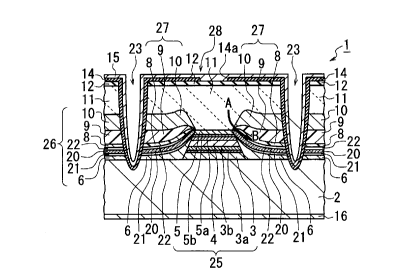
Fig. 5 is a partial cross-sectional view of a
semiconductor laser according to a first embodiment of the
invention.
Figs . 6A to 6E are partial cross-sectional views showing
the fabrication method of the semiconductor laser according to
-22-
CA 02296594 2000-03-17
the first embodiment of Fig. 5, respectively.
Fig. 7 is a graph showing the oxidation temperature
dependence of the oxidation rate of the InAlAs layer used in the
semiconductor laser according to the first embodiment of Fig. 5.
Figs . 8A and 8B are partial cross-sectional views showing
the fabrication method of a semiconductor laser according to a
second embodiment of the invention, respectively.
Fig. 9 is a perspective view of a semiconductor photonic
device according to a third embodiment of the invention, which
is comprised of a Distributed-Feedback laser and an optical
modulator.
Figs . l0A and l OB are partial plan views showing the
fabrication method of thesemiconductor photonic device according
to the third embodiment of Fig. 9, respectively.
Fig. 11 is a partial cross-sectional view of a
semiconductor photonic device according to a fourth embodiment,
which is a micro-array of eight semiconductor lasers.
Fig. 12 is a partial cross-sectional view showing the
configuration of the first one of the lasers of the semiconductor
photonic device according to the fourth second embodiment of Fig.
11.
Fig. 13 is a partial plan view showing the fabrication
method of the semiconductor photonic device according to the
fourth embodiment of Fig. 11.
-23-
CA 02296594 2000-03-17
Fig. 14 is a partial cross-sectional view showing the
fabrication method of the semiconductor photonic device according
to the fourth embodiment of Fig. 11.
Fig. 15 is a partially-cutaway, perspective view of a
semiconductor photonic device according to a fifth embodiment of
the invention, which is comprised of a semiconductor laser and
an optical waveguide serving as a spot-size converter.
Figs . 16A and 16B are partial perspective views showing
the fabrication method of the semiconductor photonic device
according to the fifth embodiment of Fig. 15, respectively.
DETAILED DESCRIPTION OF THE PREFERRED EMBODIMENTS
Preferred embodiments of the present invention will be
described in detail below while referring to the drawings
attached.
FIRST EMBODIMENT
Fig. 5 shows the configuration of a semiconductor laser
according to a first embodiment.
As shown in Fig. 5, the semiconductor laser 1 according
to the first embodiment is comprised of an n-type InP substrate
2, a strip-shaped mesa structure 25 formed on an upper surface
of the substrate 2, and a multilayer current-constricting
structure 26 selectively formed on the surface of the substrate
2 at each side of the mesa structure 25. An optical waveguide
-24-
CA 02296594 2000-03-17
forming the resonator of the laser 1 is formed in the mesa structure
25 to extend along its axial direction.
The mesa structure 25 is formed by a p-type InP cladding
layer 3 formed on the surface of the InP substrate 2, an n-type
InGaAs guiding layer 3a formed on the layer 3, an n-type InGaAs
guiding layer 3b formed on the layer 3a, an InGaAsP MQW active
layer 4 formed on the layer 3b, a p-type InGaAs guiding layer 5a
formed on the layer 4, a p-type InGaAs layer 5b formed on the layer
5a, and a p-type InP cladding layer 5 formed on the layer 5b. The
active layer 4 is formed by undoped InGaAsP barrier sublayers (not
shown) and undoped InGaAsP well sublayers (not shown) that are
alternately stacked on each other. Since the InGaAsP active layer
4 is sandwiched by the n-type InGaAs guiding layer 3b and the p-type
InGaAs guiding layer 5a, the mesa structure 25 has a double
heterojunction.
The multilayer current-constricting structure 26 is
formed by a p-type InP separation layer 6 formed on the surface
of the substrate 2 at each side of the mesa structure 25, an undoped
InGaAs buffer layer 21 formed on the layer 6, a dielectric layer
20 formed on the layer 21, an undoped InGaAs buffer layer 22 formed
on the layer 20, a p-type InP current-blocking layer 8 formed on
the layer 22, an n-type InP current-blocking layer 9 formed on
the layer 8, and a p-type InP current-blocking layer 10 formed
on the layer 9. The dielectric layer 20 serves as a first part
-25-
CA 02296594 2000-03-17
of the structure 26. The combination of the p-type InP
current-blocking layer 8, the n-type InP current-blocking layer
9, and the p-type InP current-blocking layer 10 serves as a second
part of the structure 26. Thus, the structure 26 and the n-type
InP substrate 2 constitute a so-called pnpn thyristor structure
except that the dielectric layer 20 is included therein.
A p-type InP burying layer 11 is formed to cover the mesa
structure 25 and the current-constricting structure 26, thereby
burying the structures 25 and 26. A p+-type InGaAs contact layer
12 is formed on the layer 11.
A pair of channels 23 are formed at each side of the mesa
structure 25 to be symmetrical with respect thereto. The channels
23 are formed to vertically penetrate through the contact and
burying layers 12 and 11 and the underlying structure 25, reaching
the inside of the underlying substrate 2.
A Si02 layer 14 having a strip-shaped window 14a is formed
on the p+-type InGaAs contact layer 12 to be contacted with the
inner walls of the channels 23. The window 14a is located to be
overlapped with the mesa structure 25, exposing selectively the
contact layer 12 from the layer 14. The window 14a allows a
current to vertically flow through only the parts of the layers
11 and 12 just over the active layer 4.
A p-side electrode 15 is formed on the Si02 layer 14 to
cover the window 14a. Thus, the electrode 15 is contacted with
-26-
CA 02296594 2000-03-17
the underlying contact layer 12 through the window 14a.
An n-side electrode 16 is formed on a lower surface of
the substrate 2. A driving or injection current flows vertically
from the p-side electrode 15 to the n-side electrode 16 to
penetrate through the inside of the laser 1.
With the semiconductor laser 1 according to the first
embodiment of Fig. 5, the current-constricting structure 26
includes the dielectric layer 20 as its first part and the
semiconductor current-blocking layers 8, 9, and 10 as its second
part 27 arranged vertically in series. Therefore, the unwanted
turn-on of the pnpn thyristor structure formed in the structure
26 can be prevented from occurring and at the same time, the
threshold current can be lowered. In other words, the
current-constricting structure 26 produces an effective
current-constricting performance.
Therefore, when the injection current is small, almost
all the injected current flows through the mesa structure 25
including the active layer 4 due to the existence of the second
part 27 of the current-constricting structure 26 (i.e., the
semiconductor layers 8, 9, and 10) . In this case, substantially
no leakage current flows through the structure 26.
On the other hand, when the injection current is large
for making high output, a leakage current tends to flow along the
path from the point A to the point B in Fig. 5. In this case,
-27-
CA 02296594 2000-03-17
however, even if a leakage current flows along the path from the
point A to the point B, it does not serve as the gate current of
the thyristor structure due to the existence of the first part
(i.e., the dielectric layer 20) of the current-constricting
structure 26. Therefore, a large anode current of the thyristor
structure does not flow to penetrate vertically the structure 26,
which means that the structure 26 never cause the unwanted turn-on
and that it operates normally. This is also realized when the
injection current is applied at a high temperature.
Next, a method of fabricating the semiconductor laser 1
according to the first embodiment is explained below with
reference to Figs. 6A to 6E.
First, as shown in Fig. 6A, a Si02 layer 17 with a thickness
of 100 nm is formed on the upper surface of the n-type InP substrate
2 by using the thermal CVD technique. Here, the upper surface
of the substrate 2 correspond to the ( 001 ) -plane . Then, by using
the photography and wet chemical etching techniques, the Si02
layer 17 is patterned to have a strip-shaped window 18. The width
W1 of the window 18 is, for example, set as 2 Vim. The layer 17
thus patterned serves as a mask for subsequent selective MOVPE
processes. For example, the mask 17 has a pair of strips extending
parallel to the [001] -orientation of the substrate 2, where each
of the strips has a width of 50 Eun and the pair of strips are apart
-28-
CA 02296594 2000-03-17
from each other at a distance of 1.5 Vim.
Subsequently, as shown in Fig. 6B, the p-type InP cladding
layer 3 is selectively grown by MOVPE on the exposed surface of
the substrate 2 from the mask 17. The layer 3 has a carrier
concentration of 1 x 10¹⁸ atoms/cm3 and a thickness of 100 nm. The
n-type InGaAs guiding layer 3a is selectively grown by MOVPE on
the layer 3, where the layer 3a has a carrier concentration of
1 x 10¹⁸ atoms/cm3, a bandgap wavelength of 1. 05 Vim, and a thickness
of 20 nm. The n-type InGaAs guiding layer 3b is selectively grown
by MOVPE on the layer 3a, where the layer 3b has a carrier
concentration of 1 x 10¹⁸ atoms/cm3, a bandgap wavelength of 1.13
Vim, and a thickness of 50 nm.
Furthermore, the undoped InGaAsP barrier sublayers and
the undoped InGaAsP well sublayers are successively and
selectively grown by MOVPE to be alternately stacked to each other,
thereby forming the MQW active layer 4 on the layer 3b. The layer
4 has an optical emission wavelength of 1.3 ~m and a thickness
of 90 nm.
On the active layer 4 thus formed, the p-type InGaAs
guiding layer 5a is selectively grown by MOVPE, where the layer
5a has a carrier concentration of 1 x 10¹⁸ atoms/cm3, a bandgap
wavelength of 1. 05 Vim, and a thickness of 50 nm. The p-type InGaAs
guiding layer 5b is selectively grown by MOVPE on the layer 5a,
-29-
CA 02296594 2000-03-17
where the layer 5b has a carrier concentration of 1 x 10¹⁸ atoms/cm3,
a bandgap wavelength of 1.13 Etm, and a thickness of 20 nm. The
p-type InP cladding layer 5 is selectively grown by MOVPE on the
layer 5b, where the layer 5 has a carrier concentration of 5 x
101' atoms/cm3 and a thickness of 70 nm.
Thus, the mesa structure 25 is formed on the upper surface
of the substrate 2 through a series of the selective MOVPE
processes, as shown in Fig. 6B. Due to the orientation dependence
of the growth rate of the semiconductor layers 3, 3a, 3b, 4, 5a,
5b, and 5, each side face 25a of the structure 25 forms the uniform,
smooth (111)B-plane. Accordingly, the structure 25 produces an
optical waveguide for laser oscillation that have extremely low
scattering loss. Since the mesa structure 25 is formed by the
MOVPE processes without using the wet or dry etching technique,
there is an advantage that the surfaces 25a of the structure 25
have no unevenness along its axial direction.
After the SiOz mask 17 is removed from the substrate 2,
an Si02 layer (not shown) is formed on the whole surface of the
substrate 2 to cover the mesa structure 25. The Si02 layer thus
formed is then patterned to be left only on the top of the mesa
structure 25, thereby forming the Si02 layer 19, as shown in Fig.
6C. The layer 19 is used as a mask for suppressing the growth
on the structure 25 in the subsequent selective MOVPE processes.
-30-
CA 02296594 2000-03-17
Following this, the multilayer current-constricting
structure 26 is formed by a series of selective MOVPE processes.
Specifically, first, the p-type InP separation layer 6 with a
thickness of 50 nm is selectively grown on the exposed surface
of the substrate 2 at each side of the mesa structure 25. Next,
the undoped InGaAs buffer layer 21 with a thickness of 5 nm is
selectively grown on the layer 6. An InAlAs layer 7 with a
thickness of 8 nm is selectively grown on the layer 21 for forming
the dielectric layer 20 in the later process. The undoped InGaAs
buffer layer 22 with a thickness of 5 nm is selectively grown on
the layer 7. The p-type InP current-blocking layer 8 with a
thickness of 500 nm is selectively grown on the layer 22. The
n-type InP current-blocking layer 9 with a thickness of 500 nm
is selectively grown on the layer 8. The p-type InP current-
blocking layer 10 with a thickness of 500 nm is selectively grown
on the layer 9. Thus, the multilayer current-constricting
structure 26 is completed. The state at this stage is shown in
Fig. 6C.
As shown in Fig. 6C, due to the mesa structure 25, each
of the opposing side faces l0a of the p-type InP current-blocking
layer 10 forms the uniform, smooth (111)B-plane.
Thereafter, the Si02 layer 19 on the top of the mesa
structure 25 is removed. Then, the p-type InP burying layer 11
is grown by MOVPE on the mesa and current-constricting structures
-31-
CA 02296594 2000-03-17
r
25 and 26 over the whole substrate 2, where the layer 11 has a
carrier concentration of 5 x 101' atoms/cm3 and a thickness of 1.5
Vim. The p+-type InGaAs contact layer 12 with a thickness of 300
nm is grown by MOVPE on the layer 11. The Si02 layer 13 is formed
on the layer 12 and patterned to have windows 13a for forming the
pair of channels 23. The patterned Si02 layer 13 serves as a mask
in the later etching process of forming the channels 23. The mesa
structure 28 has a width W2 of 8 Vim.
Using the patterned Si02 layer 13 as a mask, the underlying
layers 12, 11, 10, 9, 8, 22, 7, 21, and 6 and the substrate 2 are
selectively etched to form the pair of channels 23, as shown in
Fig. 6E. Thus, a mesa structure 28 is formed on the, substrate
2 between the channels 23, which includes the mesa structure 25.
As a result, the so-called double mesa structure is formed by the
mesa structures 25 and 28 on the surface of the substrate 2.
The substrate 2 having the double mesa structure is placed
in an oxidation furnace for four hours, thereby oxidizing
selectively the InAlAs layer 7 in the current-constricting
structure 26. The oxidation of the InAlAs layer 7 progresses
laterally from its exposed outer edges in the channels 23 to its
inner edges connected to the mesa structure 25. For example, when
the oxidation temperature is set as 470 °C and the thickness of
the InAlAs layer 7 is 80 nm, the oxidation rate is approximately
-32-
CA 02296594 2000-03-17
1 ~m/hour, and the oxidized region reaches the inner edges of the
layer 7 that are contacted with the mesa structure 25. The growth
of the oxidized region is automatically finished at the inner
edges of the layer 7, thereby forming the dielectric layer 20.
As a result, the layer 20 can be formed to have sufficient in-plane
uniformity at good reproducibility.
After the remaining Si02 layer 13 is removed from the
contact layer 12, the Si02 layer 14 is grown on the contact layer
12 over the substrate 2, as shown in Fig. 5. The layer 14 covers
not only the surface of the layer 12 but the inner walls of the
channels 23. The layer 13 is then patterned to have the
strip-shaped window 14a just over the strip-shaped mesa structure
25, thereby narrowing the current path running toward the active
layer 4 in the structure 25.
Finally, the p-side electrode 15 is formed on the Si02
layer 14. The electrode 15 is contacted with the contact layer
12 through the window 14a. The n-side electrode 16 is formed on
the lower surface of the substrate 2. The electrode 16 covers
the whole lower surface of the substrate 2. Thus, the
semiconductor laser 1 having the configuration shown in Fig. 5
is fabricated.
Fig. 7 shows the oxidation temperature dependence of the
oxidation rate of the InAlAs layer 7. As seen from Fig. 7, the
layer 7 can be fully oxidized by placing the layer 7 in the furnace
-33-
CA 02296594 2000-03-17
for approximately four hours or longer.
With the method of fabricating the laser 1 according to
the first embodiment, as explained above, the dielectric layer
20 can be formed in the current-constricting structure 26, so that
the layer 20 is located to be serially connected to the
semiconductor current-blocking layers 8, 9, and 10 in the
structure 26. Thus, the threshold current of the laser 1 can be
effectively lowered.
The inventors' test gave the following results about the
semiconductor laser 1 according to the first embodiment.
The length of the resonator ( i . a . , the waveguide formed
in the mesa structure 25) of the laser 1 was set as 150 Vim.
High-reflectance coating with the 70 % reflectance was applied
to the front end of the resonator and that with the 95 % reflectance
was applied to the rear end thereof . In this case, the oscillation
wavelength was 1.3 dun, the threshold current was 500 ~.tA, and the
slope efficiency was 0.65 W/A, showing that the laser 1 had
excellent characteristics.
On the other hand, the length of the resonator of the laser
1 was set as 600 ~,m. Low-reflectance coating with the 5
reflectance was applied to the front end of the resonator and
high-reflectance coating with the 95 % reflectance was applied
to the rear end thereof . In this case, the maximum optical output
-34-
CA 02296594 2000-03-17
of 400 mW was realized by injecting continuously the driving
current at 25 °C.
Since the Si02 layer 19 was formed on the p-type InP
cladding layer 5 of the mesa structure 25, as shown in Fig. 6C,
the semiconductor layers 6, 21, 7, 22, 8, 9, and 10 constituting
the current-constricting structure 26 exhibited no abnormal
growth on the substrate 2 at each side of the mesa structure 25
in their selective MOVPE processes, in other words, no
semiconductor layer that overhangs the Si02 layer 19 was observed.
Thus, uniform, smooth (111) B-planes were formed on the opposing
side faces l0a of the p-InP current-blocking layer 10, which was
found very effective in the formation process of the thick
multilayer current-constricting structure 26 by selective MOVPE.
Although the selective growth of the InAlAs layer 7 has
been very difficult, it was able to be realized in the fabrication
method according to the first embodiment if the growth conditions
such as the growth temperature and the growth rate were optimized.
For example, the growth temperature was set as 650 °C and the
growth
rate was set as 10 nm/sec. Thus, it was confirmed that the
multilayer current-constricting structure 26 was able to be
formed by a series of the selective MOVPE processes.
If the dielectric layer 20 is contacted with the MQW
active layer 4, there is a possibility that the crystallographic
property of the active layer 4 deteriorates . In the fabrication
-35-
CA 02296594 2000-03-17
method according to the first embodiment, however, such the
deterioration did not observed, because the InP layer 6 was able
to be formed by MOVPE between the mesa structure 25 and the
dielectric layer 20 with good controllability.
In the fabrication method according to the first
embodiment, the oxidation process of the InAlAs layer 7
automatically ended at the inner ends of the layer 7 near the active
layer 4 if the oxidation period was set to be excessive. As a
result, the dielectric layer 20 was made uniform along the axial
direction of the waveguide ( i . a . , the mesa structure 25 ) . It was
confirmed that this fact leaded to the good reproducibility of
the current-blocking layers 8, 9, and 10 and the uniform
performance of the element 1. According to the uniformity of the
mesa structure 25 or the active layer 4 along its axial direction,
it was confirmed that the current injection region was uniform
along its axial direction.
Unlike the prior-art photonic element 400 shown in Fig.
4B, the InAlAs layer 7 to be oxidized was not left to be overlapped
with the mesa structure 25 in the method according to the first
embodiment. Thus, it was confirmed that the current injection
efficiency was able to be prevented from lowering.
In the prior-art photonic elements 300 and 400 shown in
Figs. 3B and 4B, it is impossible to arrange other current-
blocking layer or layers with different properties from each other
-36-
CA 02296594 2000-03-17
in series with respect to the current-blocking dielectric layer
319 or 419. However, it was confirmed that this configuration
was able to be realized by the semiconductor laser 1 and its
fabrication method according to the first embodiment.
SECOND EMBODIMENT
Fig. 8B shows the configuration of a semiconductor laser
lA according to a second embodiment, which has the same
configuration as that of the laser 1 according to the first
embodiment of Fig. 5, except that a high-resistance semiconductor
layer 31 is used instead of the p-type InP separation layer 6 and
that another high-resistance semiconductor layer 32 is used
instead of the combination of the three InP current-blocking
layers 8, 9, and 10. Therefore, the explanation about the same
configuration is omitted here for simplification of description
by attaching the same reference symbols as those used in the first
embodiment in Fig. 5.
Each of the high-resistance semiconductor layers 31 and
32 is an InP layer doped with Fe, where Fe is introduced into the
layer 31 or 32 to increase the electric resistance. Thus, the
layers 31 and 32 have a so-called semi-insulating property. Since
the layers 31 and 32 have a level or levels for trapping electrons,
they exhibit higher resistance than that of layers that are not
doped with Fe.
-37-
CA 02296594 2000-03-17
It is needless to say that the semiconductor laser 1A
according to the second embodiment has the same advantages as
those of the laser 1 according to the first embodiment. The laser
lA has an additional advantage that the current-constricting
property of the current-constricting structure 26 is enhanced due
to the higher resistance of the InP layers 31 and 32.
The semiconductor laser lA according to the second
embodiment is fabricated in the following way.
The process step of forming the mesa structure 25 on the
upper surface of the n-type InP substrate 2 to that of selectively
forming the Si02 layer 19 on the top of the structure 25 are the
same as those in the fabrication method according to the first
embodiment.
After the patterning process of the Si02 layer 19 used
as a mask for the subsequent selective growth processes, the
Fe-doped InP layer 31 with a thickness of 50 nm is selectively
grown by MOVPE on the surface of the substrate 2 at each side of
the mesa structure 25, as shown in Fig. 8B. Next, the undoped
InGaAs buffer layer 21 with a thickness of 5 nm is selectively
grown by MOVPE on the layer 6. The InAlAs layer 7 with a thickness
of 80 nm for forming the dielectric layer 20 is selectively grown
by MOVPE on the layer 21. The undoped InGaAs buffer layer 22 with
a thickness of 5 nm is selectively grown by MOVPE on the layer
7. The Fe-doped InP current-blocking layer 32 with a thickness
-38-
CA 02296594 2000-03-17
of 1.2 ~.m is selectively grown by MOVPE on the layer 22. Thus,
the multilayer current-constricting structure 26A is completed.
The state at this stage is shown in Fig. 8A.
As seen from Fig. 8A, each of the opposing side faces 32a
of the Fe-doped InP current-blocking layer 32, which are located
in the vicinity of the Si02 layer 19, correspond to the uniform,
smooth (111)B-planes.
The subsequent process step of removing the Si02 layer
19 from the top of the mesa structure 25 to that of forming the
n-side electrode 16 on the lower surface of the substrate 2 are
the same as those in the method according to the first embodiment.
Thus, the semiconductor laser 1A according to the second
embodiment that have the configuration shown in Fig. 8B is
fabricated.
The inventors' test gave the following results.
The length of the resonator ( i . a . , the waveguide formed
by the mesa structure 25) of the laser lA was set as 150 Vim.
High-reflectance coating with the 80 o reflectance was applied
to the front end of the resonator and that with the 95 % reflectance
was applied to the rear end thereof . In this case, the oscillation
wavelength was 1.3 ~,m, the threshold current was 0.3 mA, and the
slope efficiency was 0.55 W/A. The obtainable modulation
frequency was as high as 30 GHz.
-39-
CA 02296594 2000-03-17
Using the above-explained method, similar to the method
of the first embodiment, it was confirmed that the laser lA was
able to be fabricated at a high fabrication yield.
THIRD EMBODIMENT
Fig. 9 shows the configuration of a semiconductor
photonic device 43, which is comprised of a Distributed-Feedback
(DFB) laser 44a and an optical modulator 44b of the electric-
field modulation type formed on the same n-type InP substrate 2.
The DFB laser 44a has the same configuration as that of the
semiconductor laser lA according to the second embodiment of Fig.
8B and a diffraction grating 45 formed below the mesa structure
25. The mesa structure 25 including the active layer 4 is commonly
used by the laser 44a and the modulator 44b, where the bandgap
wavelength of the active layer 4 is changed in value between the
laser 44a and the modulator 44b.
The reference numerals 15a and 15b denote the p-side
electrodes of the DFB laser 44a and the optical modulator 44b,
respectively. The n-side electrode 16 is commonly used by the
laser 44a and the modulator 44b.
The semiconductor photonic device 43 having the
above-described configuration according to the third embodiment
is fabricated in the following way.
First, as shown in Fig. 10A, the diffraction grating 45
is formed in the area of the upper surface of the n-type InP
-40-
CA 02296594 2000-03-17
substrate 2 for the DFB semiconductor laser 44a by a known method
such as the interference or electron-beam exposure. Here, the
length of the grating 45 is set as 400 ~m and the width of which
is set to be larger than that of the mesa structure 25.
Next, as shown in Fig. lOB, a Si02 layer is formed on the
upper surface of the substrate 2 to cover the grating 45 and then,
it is patterned to have a plan shape shown in Fig. 10B, thereby
forming a mask 46. The mask 46 is used for selective MOVPE of
the mesa structure 25 including the active layer 4. The mask 46
has a rectangular part 46a for the semiconductor laser 44a, a
rectangular part 46a for the modulator 46b, and a strip-shaped
opening 46c extending from the outer end of the part 46a to the
opposite outer end of the part 46b. The opening 46c, which is
located at the middle position of the mask 46, extends in parallel
to and overlapped with the underlying grating 45.
The part 46a has a length of 400 ~.m and a width of 115
Vim. The part 46b has a length of 200 Eun and a width of 75 ~tm.
The opening 46c has a length of 600 ~.m and a width of 15 Vim. Thus,
the part 46a has two rectangular areas of 400 ~m x 50 ~m arranged
at each side of the opening 46c, and the part 46b has two
rectangular areas of 200 ~tm x 30 ~m arranged at each side of the
opening 46c.
Using the mask 46, the mesa structure 25 is formed by
-41-
CA 02296594 2000-03-17
selective MOVPE processes in the following way while the growth
pressure is set as 150 Torr and the growth temperature is set as
650 °C.
First, the p-type InP cladding layer 3 with a carrier
concentration of 1 x 10¹⁸ atoms/cm3, a bandgap wavelength of 1.13
~tm, and a thickness of 50 nm is selectively grown on the exposed
surface of the substrate 2 from the mask 46. Then, the n-type
InGaAs guiding layer 3a with a carrier concentration of 1 x 10¹⁸
atoms/cm3, a bandgap wavelength of 1.13 Vim, and a thickness of
20 nm is selectively grown on the layer 3. On the layer 3a, the
n-type InGaAs guiding layer 3b with a carrier concentration of
1 x 10¹⁸ atoms/cm3, a bandgap wavelength of 1.2 Vim, and a thickness
of 50 nm is selectively grown.
Further, the undoped InGaAsP barrier sublayers and the
undoped InGaAsP well sublayers are successively and selectively
grown to be alternately stacked to each other on the n-type InGaAs
guiding layer 3b, thereby forming the MQW active layer 4. The
layer 4 has an optical emission wavelength of 1.55 ~,tm and a total
thickness of 90 nm.
On the active layer 4 thus formed, the p-type InGaAs
guiding layer 5a with a carrier concentration of 1 x 10¹⁸ atoms/cm3,
a bandgap wavelength of 1.2 Vim, and a thickness of 50 nm. The
-42-
CA 02296594 2000-03-17
p-type InGaAs guiding layer 5b with a carrier concentration of
1 x 10¹⁸ atoms/cm3, a bandgap wavelength of 1 . 13 ~,m, and a thickness
of 20 nm is selectively grown on the layer 5a. The p-type InP
cladding layer 5 with a carrier concentration of 5 x 101' atoms/cm3
and a thickness of 70 nm is selectively grown on the layer 5b.
Thus, the mesa structure 25 is formed to be commonly used by the
laser 44a and the modulator 44b.
The subsequent process steps are the same as those of the
method according to the second embodiment.
Through the above-explainedfabrication method according
to the third embodiment, for example, the bandgap wavelength of
the active layer 4 was able to be set as 550 nm in the laser 44a
and 1490 nm in the modulator 44b.
According to the inventors' test, with the photonic
device 43 of the third embodiment, it was found that the DFB laser
44a oscillated at a very low threshold current of 3 mA, and that
the obtainable 3-dB frequency band was 15 GHz or wider due to the
use of the high-resistance semiconductor layers 31 and 32 in the
current-constricting structure 26 of the laser 44a.
FOURTH EMBODIMENT
Fig. 11 shows the configuration of a semiconductor
photonic device 57 according to a fourth embodiment, which is a
micro-array of eight semiconductor lasers la, lb, lc, ld, le, lf,
lg, and lh formed on the n-type InP substrate 2.
-43-
CA 02296594 2000-03-17
The lasers la, lb, lc, ld, le, lf, lg, and lh are used
for the first to eighth channels 59, 60, 61, 62, 63, 64, 65, and
66, respectively. Although each of the lasers la, lb, 1c, ld,
le, lf, lg, and lh has the same configuration as that of the
semiconductor laser 1 according to the first embodiment of Fig.
5, their optical emission wavelengths are different from each
other. As an example, the configuration of the laser la is shown
in Fig. 12, where the contact layer 14 and the p- and n-side
electrodes I5 and 16 are omitted.
The semiconductor photonic device or the micro-array of
lasers 57 according to the fourth embodiment is fabricated in the
following way.
First, a Si02 layer (not shown) is formed on the upper
surface of the n-type InP substrate 2 and then, it is patterned
to have a plan shape as shown in Fig. 13 by photolithography and
wet chemical etching, thereby forming a mask 58. The mask 58 has
rectangular parts 58a, 58b, 58c, 58d, 58e, 58f, 58g, 58h, and 58i.
The part 58a located at the left-hand end in Fig. 13 has a width
PW1 of 20 Vim. The part 58i located at the right-hand end in Fig.
13 has a width PWZ of 70 ~.m. These two parts 58a and 58i are apart
from a distance PD of 71.5 Vim. The parts 58b, 58c, 58d, 58e, 58f,
58g, 58h sandwiched by the parts 58a and 58i have equal widths
and are arranged at a pitch CP of 10 Vim. The pitch CP is equal
-44-
CA 02296594 2000-03-17
to the pitch of the first to eighth channels 59 to 66. Adjoining
two ones of the parts 58b, 58c, 58d, 58e, 58f, 58g, 58h are apart
from equal distances CW of 1.5 Vim. The distance CW is equal to
the width of each of the channels 59 to 66.
Subsequently, using the mask 58 thus formed, the mesa
structures 25 for the first to eighth lasers la, lb, lc, 1d, le,
lf, lg, and lh are formed on the surface of the substrate 2 by
selective MOVPE, as shown in Fig. 14. The MOVPE is carried out
at the growth pressure of 150 Torr and the growth temperature of
650 °C. The state at this stage is shown in Fig. 14.
Thereafter, through the same process steps as those in
the method according to the first embodiment, the Si02 layer 19
is selectively formed on the tops of the first to eighth mesa
structures 25, the multilayer current-constricting structure 26
is formed at each side of each of the mesa structures 25, the
burying layer 11, the contact layer 12, and the Si02 layer 14 are
formed. Next, to make it possible to separately drive the eight
lasers la, lb, lc, ld, le, lf, lg, and lh, the eight p-side
electrodes 15 are formed on the tops of the respective mesa
structures 28. Finally, the common n-side electrode 16 is formed
on the lower surface of the substrate 2. Thus, the semiconductor
photonic device (i.e., the semiconductor micro-array lasers) 57
according to the fourth embodiment is completed.
With the method of fabricating the photonic device 57
-45-
CA 02296594 2000-03-17
according to the fourth embodiment, the mask 58 is asymmetric with
respect to its center, in other words, the end parts 58a and 58i
of the mask 58 are not equal in width to each other, as shown in
Fig. 13. Therefore, the optical emission wavelength of the lasers
la, lb, lc, 1e, lf, lg, and lh for the first to the eighth channels
59 to 66 increases in steps . As a result, for example, the optical
emission wavelengths of the lasers 1a, 1b, lc, le, 1f, lg, and
lh can be set to vary from 1520 nm for the first channel 59 to
1600 nm for the eighth channel 66 at approximately equal intervals
within the narrow area of approximately 80 Vim. In other words,
the eight lasers la, lb, lc, le, lf, lg, and lh having the
optical-emission wavelength difference of 80 nm can be arranged
in the narrow area of approximately 80 Vim.
The inventors' test gave the following results.
The length of the resonator ( i . a . , the waveguides formed
by the mesa structures 25) of the eight lasers la to lh was set
as 400 Vim. The front and rear ends of the resonator were set to
be cleavage planes . In this case, the threshold currents of all
the lasers la to lh were as low as 4 mA or less, which is due to
the good uniformity and the high performance of the current-
constricting structures 26 of the lasers la to lh. This means
that the advantages of the invention exhibits conspicuously if
the invention is applied to an array of semiconductor photonic
-4 6-
CA 02296594 2000-03-17
elements, such as the device 57.
In the above-described fourth embodiment, the mask 58 has
the asymmetric pattern as shown in Fig. 13. However, the
invention is not limited to this case. The end parts 58a and 58i
of the mask 58 may have equal widths, in which the lasers la to
lh have equal optical emission wavelengths. Similarly, the
optical emission wavelengths of the lasers 1a to lh may have a
distribution that they are maximized or minimized at the laser
or lasers located at the middle position.
Needless to say, the number of the lasers forming the
array may be optionally changed.
FIFTH EMBODIMENT
Fig. 15 shows the configuration of a semiconductor
photonic device 77, which is comprised of the semiconductor laser
1 according to the first embodiment of Fig. 5 and an optical
waveguide 78 serving as a spot-size converter.
The waveguide 78 has the same configuration as that of
the mesa structure 25 and the current-constricting structure 26
of the laser 1. However, as seen from Fig. 15, the thickness of
the waveguide 38 decreases gradually from the connection point
to the laser 1 to the light-emission end of the device 77. Also,
the bandgap wavelength of the active layer 4 in the structure 25
decreases gradually from the connection point to the laser 1 to
the light-emission end of the device 77.
-47-
CA 02296594 2000-03-17
Moreover, the p-side electrode 15 extends to be
overlapped with the waveguide 78 by a width of approximately 50
Vim, thereby injecting the driving current for the laser 1 into
the part of the waveguide 78. Thus, there is an additional
advantage that optical absorption loss can be prevented from
increasing at the transition region where the composition of the
active layer 4 changes between the laser 1 and the waveguide 78.
The semiconductor photonic device 77 according to the
fifth embodiment is fabricated in the following way.
First, a Si02 layer (not shown) is formed on the upper
surface of the n-type InP substrate 2 and then, it is patterned
to have a plan shape as shown in Fig. 16A by photolithography and
wet chemical etching, thereby forming a mask 79. The mask 79 has
two parts 79a and 79b and a strip-shaped opening 79c between the
parts 79a and 79b. The parts 79a and 79b have symmetric plan
shapes with respect to the opening 7 9c . The part 7 9a has a width
of 50 ~m in the laser area for the laser 1 and a varying width
of 50 um to 5 Etm in the waveguide area for the waveguide 78. The
waveguide area includes a tapered area in which the width
decreases from 50 ~,m to 5 Vim. The laser area has a length of 300
~,tm and the waveguide area has 200 Vim, where the length of the
tapered area is 100 Vim. The opening 79c has a width of 1.5 ~,m.
-48-
CA 02296594 2000-03-17
Subsequently, using the mask 79 thus formed, the mesa
structure 25 used for the laser 1 and the waveguide 78 is formed
on the surface of the substrate 2 by selective MOVPE, as shown
in Fig. 16B. The MOVPE is carried out in the same condition as
that of the first embodiment. The state at this stage is shown
in Fig. 16B. Due to existence of the tapered area in the mask
79, the thickness of the mesa structure 25 decreases gradually
in the waveguide area.
Thereafter, through the same process steps as those in
the first embodiment, the Si02 layer 19 is selectively formed on
the top of the mesa structure 25 thus formed, the multilayer
current-constricting structure 26 is formed at each side of the
structure 25, and then, the burying layer 11, the contact layer
12, and the Si02 layer 14 are formed successively. Next, the
p-side electrode 15 is formed on the top of the mesa structure
28 in the laser 1 so as to be overlapped with the waveguide 78
in the waveguide area. Finally, the n-side electrode 16 is formed
on the lower surface of the substrate 2. Thus, the semiconductor
photonic device (i. e. , the semiconductor laser) 77 according to
the fifth embodiment is completed.
With the method of fabricating the photonic device 57
according to the fifth embodiment, not only the side faces 25a
of the mesa structure 25 but also the side faces of the waveguide
7 8 are formed to correspond to the smooth ( 111 ) B-planes . Also,
-49-
CA 02296594 2000-03-17
the height or thickness of the waveguide 78 decreases gradually
along its axial direction. As a result, the optical emission
wavelength of the active layer 4 decreases gradually, thereby
reducing the absorption of the propagating light in the waveguide
78. This means that the waveguide 78 has low scattering loss.
The inventors' test gave the following results.
The front end of the device 1 was set to be a cleavage
plane and a high-reflectance coating with the 95% reflectance was
applied to the rear end thereof. In this case, the threshold
current of the laser 1 was 4 mA and 12 mA at 25 °C and 85 °C,
respectively.
Moreover, the emission angle of the emitted light from
the front end of a popular laser element is 30° or greater in both
the lateral and vertical directions. However, unlike this, the
emission angle of the emitted light from the front end of the device
77 was as narrow as 10°. This was because the tapered waveguide
78 was integrated with the laser 1 on the InP substrate 2 and the
height of the waveguide 78 decreased gradually toward the output
end of the light, thereby making the optical confinement weak to
thereby expand the emission field of the light. Accordingly, the
difference of the field from that of an optical fiber became small
and as a result, there arose an additional advantage that optical
coupling between the device 77 and an optical fiber was able to
-50-
CA 02296594 2000-03-17
be improved. For example, the obtainable minimum coupling loss
of the device 77 with a single-mode optical fiber was improved
to be 1.5 dB.
In the above-explained first and second embodiments, the
laser 1 or lA is used. However, any other type of semiconductor
photonic elements such as a distributed Bragg-reflection laser
or DFB laser and semiconductor optical amplifier may be used.
In the above-explained first to fifth embodiments, the
dielectric layer 20 serving as the current-blocking layer is
formed by oxidizing an InAlAs layer. However, the invention is
not limited thereto. An AlAsSb layer, the combination of an AlAs
sublayer and an InAlAs sublayer with the superlattice structure,
or the combination of an AlAs sublayer and an AlAsSb sublayer with
the superlattice structure may be used for this purpose.
Although the laser element is combined with an optical
modulator or an optical waveguide, it may be combined with any
other optical element, such as a semiconductor optical switch and
a semiconductor optical amplifier.
The number of the dielectric layer 20 of the current-
constricting structure 26 is unity in the above embodiments.
However, it may be set as two or more.
While the preferred forms of the present invention have
been described, it is to be understood that modifications will
be apparent to those skilled in the art without departing from
-51-
CA 02296594 2000-03-17
the spirit of the invention. The scope of the present invention,
therefore, is to be determined solely by the following claims.
-52-