Note: Descriptions are shown in the official language in which they were submitted.
CA 02296921 2000-O1-21
C. J.Chrin - 4 - 2 - 21 1
A LARGE COMBINED BROADBAND AND NARROWBAND SWITCH
Related Application:
This Application is related to an Application entitled,
"Flexible Telecommunications Switching Network" being filed by
C. J. Chrin and M. J. Zola, concurrently, with this Application
and assigned to the same assignee, and is also related to a
Patents Application entitled, "Enhanced Telecommuni-cations
Switching Unit, Serial Number 08/856,842, filed May 15, 1997,
by C. J. Chrin and M. J. Zola, and assigned to the same
assignee as this Application.
Technical Field:
This invention relates to digital telecommunications
switching systems, and more specifically, to narrowband and
broadband digital telecommunications switching systems.
Problem:
As is well known, the demands for telecommunications
services are changing rapidly. Many of these demands are for
services such as video, which require a much broader band than
the conventional audio band. The combination of cable
television distribution systems with telephone and other
customer premises equipment telecommunications systems, is
making more and more available a loop plant capable of
transmitting broadband signals to individual customers. At the
same time, the development of switching systems which handle
both broadband and narrowband signals in an efficient and
integrated way, has not kept pace with this demand.
Accordingly, a problem of the prior art is that there is no
satisfactory large switching system for processing both
narrowband and broadband traffic efficiently and an integrated
fashion.
CA 02296921 2000-O1-21
C. J.Chrin - 4 - 2 - 21 2
Solution:
The above problem is solved, and an advance is made over
the prior art in accordance with this invention, wherein a core
central network receives inputs in a standard format from a
plurality of connecting modules, and switches these signals
among the modules.. In order to handle a large amount of
broadband traffic efficiently, these signals each carry a
substantial number of base band channels combined into a single
signal. In accordance with Applicant's preferred embodiment,
the standard signal is a signal that carries 2.048 Mb per
second payload, the equivalent of 32 DSO voice channels. Each
such signal is switched through the central core entity without
changing the information in the payload.
In accordance with one feature of Applicants' invention,
when a narrowband signal, i.e., a single voice channel, is to
be switched through the core, this narrowband signal occupies
only a single DSO payload, with the rest of the signal being
occupied by "fill" bits. Advantageously, this allows
individual voice channels to be switched through the central
core from any connected module to any other connected module.
In accordance with Applicants' preferred embodiment, the
modules connected to line and trunk signals convert these
signals into standard format signals. These modules include a
microprocessor based switch, wherein the microprocessor
receives input pulse code modulated signals generated by
standard line and trunk interface cards, and converts these
into standard intermediate stage signals, and switches signals
from particular lines and trunks to a standard signal destined
for the appropriate module at the other end. In addition,
output interface units for interfacing between facilities such
as SONET/SDH, (Synchronous Optical Network/Synchronous Digital
Hierarchy) facilities, and the cores which are connected to the
core switch, with the communications being the standard
signals. These output interface units convert between the
standard signal and an ATM, or IP signal, for transmission over
virtual channels of the SONET facilities.
The standard signals in this embodiment are vT2 signals
CA 02296921 2000-O1-21
C. J.Chrin - 4 - 2 - 21 3
and carry 32 64Kbit channels, and are further characterized in
the discussion of Figures 17 - 20.
Advantageously, using 1999 technology, a core network for
supporting 12288 (768 x 16), VT2 signals, can be housed on a
sing7_e custom silicon chip. This is a great advantage compared
to disbursing this .,circuitry over many chips, since intra-chip
connections do not require interface circuits, and can use the
very narrow circuit interconnection lines allowable on a
silicon chip. Advantageously, by allowing one narrowband
signal to occupy to a full VT2 signal on a full
interconnectivity among modules connected to the core network,
' is possible without requiring the core network to switch
anything other than VT2 signals.
In accordance with another feature of Applicants'
invention, connections to prior art modules is made possible.
Prior art modules such as the communication module of a SESS~
switch, manufactured by Lucent Technologies Inc., communicate
via proprietary link signals, which are encapsulated at the
input of the core network into VT2 signals. These NCT links
can carry both narrowband and broadband signals. The
communication module can be connected to a switch module of a
5ESS~ switch.
In accordance with another aspect of Applicants'
invention, a group of modules are interconnected by a plurality
of center stage modules as in a Clos network, a well-known
arrangement for guaranteeing absence of blocking from any input
to any output. Advantageously, a large non-blocking network is
made feasible by this arrangement.
Brief Description of the Drawinq(s):
Figure 1 is a block diagram of a microprocessor
based time-slot interchange module;
Figure 2 is a block diagram of the internal
microprocessor architecture of the TSI module;
Figure 3 is a block diagram of memory and buffer layouts
for the TSI module;
CA 02296921 2000-O1-21
- C. J.Chrin - 4 - 2 - 21 4
Figure 4 is a flow diagram of the program for
controlling the TSI module;
Figure 5 shows modifications of the program of
Figure 4, for the case in which the multiple sub-frames
are encountered between each frame synchronizing pulse.
i
Figure 6 illustrates the program for controlling the
microprocessor, acting as a time multiplexed switch;
Figure 7 shows the program for a TSI, wherein groups
of time-slots are bundled and switched as a bundle;
Figure 8 illustrates a cell header for an
asynchronous transport method, (ATM), cell header;
Figure 9 illustrates the basic operation of the
processing of an ATM cell;
Figure 10 is a programmer's module, illustrating the
layout of memory for a microprocessor acting as a ATM
switch;
Figure 11 is a flow diagram, illustrating the
operation of the input processing of a microprocessor ATM
switch;
Figure 12 illustrates the processing of the output
queue of the microprocessor program for an ATM switch;
Figure 13 illustrates the process of processing ATM
cells to output links of a microprocessor ATM switch;
Figure 14 is a block diagram, illustrating the
arrangement for expanding the size of a microprocessor
control switch through replication of microprocessor
complexes;
Figure 15 shows a CLOS network of switching
microprocessors;
3o Figure 16 is a conceptual diagram, illustrating a 3-
stage network for use as a combined circuit and packet
CA 02296921 2000-O1-21
C. J.Chrin - 4 - 2 - 21 5
switch;
Figure i7 is a detailed block diagram of such a 3-
stage network;
Figure 18 shows details of the connections to the
central fabric of Figure 17;
Figure 19 shows arrangements for interconnecting a
plurality of the central stages of Figure 17; and
Figure 20 is a more detailed block diagram of the
core fabric of Figure 17.
General Description:
The descriptions of Figures 1 - 14 relate to single-stage
networks for performing the TSI function, TMS function, and for
performing within the same module, also functions of packet
switching for switching ATM signals, and signals in the
Internet Protocol, (IP). Figure 14 shows how a group of
smaller modules can be paralleled to perform the function of a
larger module. Figure 15 shows a Clos network made of the
modules described earlier. Figure 16 is a conceptual diagram,
illustrating a 3-stage network for use as a combined circuit
and packet switch. The subject matter of Figures 17 - 20,
which is the bulk of the claimed subject matter of this
Application, uses the modules described in the earlier part of
the Application, but interconnects these modules with a novel
type of center stage, to create a very large switch.
Detailed Description:
This specification describes an arrangement for, and
method of implementing multiple hardware functionality by
appropriate software on a Reduced Instruction Set Computer,
(RISC) microprocessor. Although this is described in terms of
a RISC microprocessor, other types of microprocessor
implementations, (e. g., Complex Instruction Set Computer),
(CISC) can also be used. Multiple functions can reside on the
same microprocessor simultaneously, or only a single function
can be provided. The determination of the type of treatment
CA 02296921 2000-O1-21
C. J.Chrin - 4 - 2 - 21 6
each input and/or output shall receive, (e. g., Time-Slot
Interchange (TSI), Time Multiplexed Switch (TMS), Cross-
connect (XCON), Asynchronous Transfer Mode (ATM) Switch,
Internet Protocol (IP) Router, Dynamic Synchronous Transfer
Mode (DTM), Frame Relay (FR) switch, etc.), is determined by,
and can be reconfigured by, software control. Conversion
between input to output formats can also be provided, e.g., a
circuit switched PCM format can be converted to/from ATM
format. A method is identified for using multiple
microprocessors for building very large configurations for
applications which do not fit on a single microprocessor.
' Other advantages include:
1. Little or no VLSI Required - faster time
to market (eliminates development).
2. Microprocessor Self Test - (reduces
investment in chip and board test tools).
3. Follows Moore's Law Technology Curve
Directly - (graceful evolution).
4. Core Architecture Usable by Multiple
Applications.
5. Results in Lower Development Effort
(contributed to by all of the above).
Among the basic techniques used are the following:
1. Input bit streams are clocked into serial
in, parallel out shift registers and then
read out in parallel onto the
microprocessor data bus under control of
the microprocessor address bus.
2. This data, is then stored in the internal
microprocessor cache memory which may be
expanded by a level 2 cache on or outside
the microprocessor chip, and/or an
auxiliary memory outside the
CA 02296921 2000-O1-21
C . ,1. Chrin - 4 - 2 - 21 7
microprocessor chip, and is manipulated
' under stored program control in such a
way as to provide the desired switching
function.
3. The more frequently used sections of the
stored .program are, advantageously,
stored in caches.
4. The resulting outputs are read out in
parallel to parallel in, serial out shift
registers, and then clocked out onto
serial bit streams.
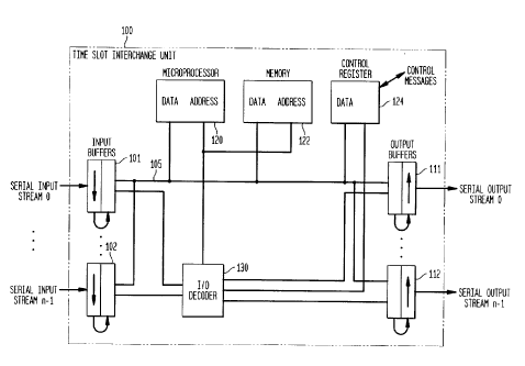
Figure 1 is a block diagram of the basic system
architecture. The heart of the system is a Microprocessor
containing on board program and data caches and external
Input/output consisting of serial to parallel shift registers
as Input Buffers, and parallel to serial shift registers as
Output Buffers. An Input/output decoder under the control of
the Microprocessor selects the Input Buffer which puts its data
on the Data Bus or the Output Buffer, which reads the data from
the data bus. The Control Register is used to receive and
transmit control messages from/to the outside world. The
external Memory is used to store back-up and maintenance code,
as we:l1 as data structures which are too large to fit into the
cache. Microprocessor software is used to provide switching
functionality which has traditionally been provided by hardware
implernentation. Thus, multiple diverse functions can be
provided concurrently by a single microprocessor architecture.
By changing the resident software, different sets of functions
can be provided.
Figure 1 shows the input and output data streams of a
time-slot interchange unit 100 in accordance with Applicant's
invent=ion. In one preferred embodiment of Applicant's
invent=ion,. a 300 MHZ PowerPC~k EC 603e microprocessor,
manufactured by the Motorola Corporation, can switch 192 serial
input and output streams, each consisting of 32 time-slots at a
bit rate of 2.048 Mbits per second. The input comprises n
serial input streams, stream zero being connected to input
CA 02296921 2000-O1-21
C. J.Chrin - 4 - 2 - 21 8
buffer 101, . . . , and serial input stream, n - 1, being
' conne~~ted to input buffer 102. The first input stream is
collected in a shift register of input buffer 101, and then
transmitted in parallel, sequentially to a four-stage, sixty
four bit per stage, buffer. The last stage of this buffer is
connected to a series of sixty-four tri-state bus drivers for
driving parallel bu$ 105. Also connected to parallel bus 105,
are n output buffers 111, . . . , 112. These outputs buffers
also comprise four-stage, sixty-four bit registers, the input
stage of which is connected to sixty-four bus receivers
connected to bus 105, and the output stage of which is
connected to a shift register for generating a serial output
stream. Also connected to bus 105, is microprocessor 120 which
accepts inputs in bursts of 256 bits as four associated 64-bit
data bus reads, from each of the n input buffers 101, . . . ,
102, under the control of the program stored in the
microprocessor. Similarly, the microprocessor delivers bursts
of 256 bits as four associated 64 bit data bus writes to each
of the' n output buffers after having generated the output burst
through the reading of the inputs under the control of a
contrc>1 map, and of the program of the microprocessor.
An I/0 decoder unit 130, under the control of the
microprocessor, is used to gate the tri-state outputs of the
input buffers onto the bus, and to gate the output of the bus
into t=he n output buffers 111, . . . , 112. The I/O decoder
receives inputs from the microprocessor address bus.
Also connected to bus 105, is a memory 122 for storing
infrequently used data and program text such as data required
for performing tests or diagnostics, non-cached TSI code, and
as a backup for data stored in the microprocessor cache, such
as the microprocessor program text and the path memory. Also
connected to bus 105, is control register 124, which interfaces
with a call processing controller or other switches of the
telecommunications network, and receives and transmits control
messages.
Figure 2 is a block diagram of those key parts of the
microprocessor which are pertinent to the understanding of
Applicant's invention. The microprocessor contains a program
CA 02296921 2000-O1-21
C. J.Chrin - 4 - 2 - 21 9
cache 201 for storing the control program which controls the
operations of the time-slot interchange unit. The output of
the program cache goes to an instruction queue 203 for storing
a plurality of instructions in order to allow for the rapid
execution of simple loops that is made possible using
pipelining techniques. The instruction queue interacts with an
instruction Control Block 205, to deliver the appropriate
instructions to arithmetic and logic unit (ALU) 207. The ALU
executes its received instructions and operates to perform the
steps required by the instruction, by controlling load store
unit 213, which in turn accesses a data cache 211. ALU 207
also controls a group of internal registers 215, for short term
storage, and for the control of the microprocessor. A bus
interface 217 communicates between bus 105, (Fig. 1), and
within the microprocessor with the data cache 211, and for
changes or back-up in the software, also communicates with
program cache 201.
Figure 3 shows pertinent memory data stored in data cache
211 of microprocessor 120, and in hardware registers. The
contents of the data cache contain, among other items, the
data received from input buffers 101, . . . , 102, and the data
to be delivered to output buffers 111, . . . , 112. Data
received from the input buffers 101, . . . , 102, is stored in
TSI buffer 301 or 303. The data from the various input buffers
is stored sequentially in one of these buffers in Applicant's
preferred embodiment. In order to handle nx64 kilobit per
second connections, the TSI buffer contains buffer 301, and a
second buffer 303, for storing another frame of this serial
input data. Buffers 301 and 303 are used alternately. control
map 311 is used to control the reading of the contents of TSI
buffers 301 or 303 in order to generate an output for storage
in the TSI output buffer 321, for transmission to one of the
output buffers 111, . . . , 112. TSI write pointer 315 is used
to keep track of where the next input from one of the input
buffers 101, . . . , 102, is to be stored in TSI buffer 301 or
303. Control pointer 313 is used to point to the appropriate
portions of control map 313 in order to control accessing the
TSI buffer in order to obtain the time-slots that are required
to fill the TSI output buffer 321. Input buffer count 331 is
CA 02296921 2000-O1-21
C. J.Chrin - 4 - 2 - 21 10
used to control the cycling for accepting inputs from the
appropriate one of the n input buffers 101, . . . , 102,
selected by input buffer address register 332, and output
buffer count 333 is used to control the distribution of an
output collected in TSI output buffer 321 to one of the n
output buffers 111, . . . , 112, selected by output buffer
address register 334. Link status memory 341 is used to
identify any of the n input links or any of the n output links
that are out of service. This status can be checked prior to
accepting an input from one of the n input buffers 101, . . .,
102, or prior to sending an output to one of the output buffers
111, . . . , 112.
The control map is altered under the control of the
program of the microprocessor when the microprocessor receives
a control message from connect request register 351 within the
control register 124 of Figure l, the control message
representing a request to establish or disconnect a connection
in the time-slot interchange unit. The process of controlling
the control map is well known in the prior art.
Figure 9 is a flow diagram describing the operation of
the program for implementing a time-slot interchange (TSI) in
accordance with Applicant's invention. The process starts with
the microprocessor waiting for a frame synchronization pulse
(Block 401). When the frame synchronization pulse arrives, it
signals the beginning of the synchronized loading of the input
buffers 101, . . . , 102, from the serial input streams, and
triggers several initialization steps. The memory write
address, (TSI write pointer 315), is initialized, (Action Block
402), so that the correct location in the TSI buffer 301 and
303 i.s established for writing the information from the input
buffers 101, . . . , 102. The double buffering offset is
toggled (Action Block 403), to choose either frame memory 301
or 303 in the TSI buffer for storing the input data on
alternate frames. The microprocessor then waits for an input
buffer loaded signal, (Action Block 404), which establishes
that the buffers 101, . . . , 102, are full, and then the input
buffer address is initialized, (Action Block 405), to point to
the first input buffer 101. In order to guarantee that Action
CA 02296921 2000-O1-21
C. J.Chrin - 4 - 2 - 21 11
Block 406 reads new data from the input buffer, and not stale
' cached data from a previous cycle, Action Block 405
invalidates the cache data associated with the input buffer
address before initiating the read. The input buffer pointed
to by the input buffer address is then read, (Action Block
406), in a burst as four connected 64 bit data bus operations,
and stored in the imicroprocessor cache memory in either TSI
buffer 301 or 303, depending on the double buffering offset.
Test 407 determines whether all inputs for this frame have been
written. If not, then the buffer address is incremented,
(Action Block 409), and the next buffer is read into the TSI
buffer, (Action Block 406, previously described). This loop
is continued until the results of test 407 indicates that all
inputs for this frame have been written.
At this point, the TSI read cycle begins. The output
buffer address 334 is initialized, (Action Block 421), the TSI
output buffer address is initialized, (Action Block 423), and
the control map pointer 313 is initialized to point to the top
of the control map, (Action Block 425). The contents of the
control map are read to an index register, (Action Block 427),
and the index register is used to read the eight bit time-slot
from the TSI buffer, (Action Block 429) ; (frame 301 or 303 is
accessed depending on the double buffering offset established
in Action Block 403) . The read byte is then written into the
TSI output buffer in the cache, at the appropriate offset, (TSI
output buffers 321), (Action Block 431), determined by which of
the 32 bytes is being written. Test 433 is used to determine
whether 32 bytes have been written; if not, Action Block 427 is
re-entered, and the loop repeats Action Blocks 427, 429, 431.
When 32 bytes have been written, as indicated by a positive
result of test 433, then 32 bytes are written from the cache,
(Action Block 441), by a data cache block flush operation in a
burst of four connected 64 bit data bus writes into the output
buffer 111, . . . , 112, specified by the output buffer address
334. Test 443 determines whether all outputs have been
written. If not, then the TSI output buffer read address is
re-initialized, (Action Block 445). The output buffer address,
(output buffer address 334), is then incremented, (Action Block
447), and the loop for writing into the output buffer is re-
CA 02296921 2000-O1-21
C. J.Chrin - 4 - 2 - 21 12
entered in Action Block 427. If test 443 indicates that all
outputs have been written, then the work for this frame is
finished, and the processor goes back to Block 401 to wait for
the next frame synchronization pulse.
The above flow chart provides double buffering for all
time-slots whether ;they represent nx64 kilobits per second
signals such as 256 kilobit data, or a single 64 kilobit per
second voice or data time-slot. If the additional frame delay
introduced by the double buffering is not desired for the
single 64 kbit/sec voice or data time-slot, then the flow chart
can be modified to provide selective double buffering, i.e.,
' the single voice or data time-slot is not double buffered.
Such single buffered time-slots are marked in the control map
311, which causes the time-slot to be read from the other one
of the two TSI buffer frames 301 and 303, by negating the
effect of the double buffer offset. Thus, single buffered
time-slots may be read out of the opposite frame from the
double buffered time-slots.
Generalized TSI Flow
The flow chart shown in figure 4 is transversed only once
per frame because each of the serial input streams was assumed
to consist of 32 time-slots, which in the present
implementation is written into the microprocessor cache in a
single 32 byte burst, as described when Action Block 406 was
discussed. Relatively simple modification of Figure 4 is
required and illustrated in Figure 5, in order to accommodate
higher bandwidth serial links:
(1) Another decision state 451 is required
after the "Yes" output of decision state
443 in Figure 4. This determines whether
the entire frame of time-slots has been
processed. If "Yes", we return to the
wait state of Block 401. If "No", we
return to the wait for input buffer
loaded block 404 for the next burst of 32
time-slots.
CA 02296921 2000-O1-21
C. J.Chrin - 4 - 2 - 21 13
(2) The initialize read control map pointer,
Action block 425, is moved out of the TSI
read loop to the beginning of the TSI
write cycle, (after the initialized
memory write address, Action Block 402),
since the entire frame has not yet been
written.-'
The RISC microprocessor hardware of Figure 1, the block
diagram of Figure 2, and the programmer data model of Figure 3,
can also be used for implementing a Time Multiplexed Switch,
(TMS). The basic difference is that a TSI application requires
the .storing and maintaining in memory of either one or two
frames of time-slots, (single or double buffered applications),
whereas a TMS application requires the switching of the time-
slots as soon as possible after they appear at the input to the
TMS. This means that after the serial input streams appearing
at 101, . . ., 102, (which have been written into the TSI
buffer of Figure 3), are read out to the serial output streams
111, . . . , 112, their storage in the TSI buffer is no longer
necessary. Therefore, subsequent write bursts into this buffer
during the frame interval can overwrite the old data. This
means that less memory is required for the TMS application than
the TSI application, since only 32 bytes, (the write/burst
size), per serial input are required rather than one or two
frames of memory. Also, double buffering is not required for
nx64 kbits per second, because the time-slots are read out
immediately, and thus, there is no possibility of the time-
slots getting out of sequence.
Figure 6 is a flow chart for implementing a TMS. It is
similar to the TSI basic flow chart (Figure 4), and
incorporates the changes described earlier for generalized TSI
flow, as well as the differences described above for a TMS. To
help the reader, the same action is given the same number as in
Figure 4. For a TMS, high bandwidth facilities, much larger
than the 2.048 Mbits per second assumed for the basic TSI flow
chart, are required. This requires the addition of test 449 in
Figure 6 in order to handle the entire frame, and moving the
initialize read control pointer, (Action Block 425), from the
CA 02296921 2000-O1-21
C. J.Chrin - 4 - 2 - 21 14
TSI read cycle to the frame initialization portion near the
beginning of TMS write cycle of Figure 6. These two steps are
the came as those described for a generalized TSI flow.
To implement TMS functionality, the only two changes to
the flow chart are:
(1) Move Action Block 402 from the frame
initialization portion of the TSI write
to the buffer loaded inner loop, so it
can overwrite the previous burst, since
as described in the previous paragraph,
this data has already been output; and
(2) eliminate Action Block 403, which is used
to implement double buffering. The TMS
flow chart of Figure 6 implements the
time multiplexed switching function.
A variation on writing the input buffers 101, . . . ,
102, sequentially into cache, is that instead of taking a 32
byte burst from a single input buffer, 8 bytes from each of
four input buffers are written. This has the advantage of
reducing the number of bytes of buffering required by input
buffers 101, . . . , 102, from 32 bytes to 8 bytes per buffer.
Taking 16 bytes from each of two buffers can also be
implemented.
Figure 7 is a flow diagram illustrating the operation of
the system when used for switching groups of time-slots at a
time. This use would be for replacement of a digital cross-
connect (XCON), such as the DACS (Digital Access And Cross-
Connect System), systems manufactured by Lucent Technologies.
Blocks 461, 463, 465, and 467, replace the functions
carried out by Blocks 429, 431, and 433, in Figure 6. In the
implementation described in Figure 7, only Blocks 461 and 463
are repeated 8 times. In the final repetition, 465 and 467 are
shown, but instead of using the loop, the program is written
in-line. Action Block 461 is essentially equivalent to Action
Block 429 of Figure 6, and Action Block 463 is essentially
CA 02296921 2000-O1-21
C. J.Chrin - 4 - 2 - 21 15
equivalent to Action Block 431 of Figure 6; however, instead of
having a test of 433, the code is simply repeated 8 times prior
to entering Action Block 441.
The above flow chart described an eight bit time-slot
where a byte quantity is read and written in Action Blocks
429
and 431. Sixteen and 32 bit time-slots can easily be
accon~nodated with a straightforward substitution of half
word
or full word microprocessor instructions, for the corresponding
load and store byte instructions. The time-slot width can
be
further generalized to include group switching, where
contiguous time-slots are switched as a group using load/store
' string instructions in Action Blocks 429 and 431, to transfer
a
sequence of time-slots. The total number of bytes of switched
information per unit of time, increase with increasing time-
slot width or group size, since the loop overhead of Action
Blocks 427 through 433 is reduced proportionally relative
to
that of a byte wide time-slot. This is very efficient for
switching a 32 time-slot PCM (E1) facility, for implementing
a
cross-connect. Some group sizes like that of a T1 facility
of
24 byte wide groups, might be most efficiently switched by
padding the 24 time-slots to a 32 byte group. Groups can be
concatenated contiguously to form higher bandwidth rates,
such
as DS3 at the output of the output buffers; this is especially
useful for performing the function of a digital access and
cross-connect system.
The block diagram of Figure 1 can also be used to
implement an ATM Switch. Figure 8 shows the structure of an
ATM cell header. The ATM cell might be most efficiently
switched by padding the 53 time-slots into a 64 byte group.
This requires some control logic in the Input Buffers and
Output Buffers. The generic flow control bits 5 - 8 of octet 1
are used for overall control to prevent an ATM system from
being overloaded. The virtual path identifier is split across
the first four bits of the first octet, and the last four bits
of the second octet. The virtual path identifier identifies a
user. All virtual channels of the same user use the same
virtual path identification. The virtual path identifier is
the primary identifier used for switching ATM cells within a
CA 02296921 2000-O1-21
C. J.Chrin - 4 - 2 - 21 16
switch, and for identifying incoming ATM cells so that they can
be switched to the appropriate destination. The virtual
channel identifier, (the first four bits of octet 2, all of
octet 3, and the last four bits of octet 4), is used by the
user to identify a specific communication among a plurality of
the communications between the end users; the specific
communication resides on a specific channel. The first four
bits of octet 4 are the payload type (2 bits), one bit reserved
for future use, and a cell loss priority bit. The cell loss
priority bit is used to help determine whether a particular
cell may be discarded in case of overload. Finally, the header
error control octet is a cyclic redundancy check (CRC) over the
header.
Figure 9 is a functional overview of the software control
components of the ATM Switch. They consist of a CRC Check,
Input Link Control, VPI/VCI Processing, Shaping, Quality of
Service (QOS) Processing, Output Link Control, and CRC
Gener<~te . The cyclic redundancy check, (Action Block 901 ) , is
performed on the header of each ATM cell as it enters the
systern. Input link control, (Action Block 903), brings
incoming data into the memory of the microprocessor. VPI/VCI
processing, (Action Block 905), finds a VPI/VCI data block
which contains an Input VPI/VCI indication, an Output VPI/VCI
indication, and a Quality of Service, (QOS), pointer. Test
907 is used to determine whether a shaping test is necessary.
ShaplIlg tests are not performed on every cell, but typically,
on every tenth cell. If this is a cell that requires the
performance of the shaping function, this shaping function is
executed, (Action Block 909). The shaping function determines
whether the peak or the average allowed data rate is being
exceeded. If so, the shaping function introduces a throttle to
the transfer of information, which is regulated by putting
packet=s into a shaping queue with limited size, so that if the
peak rate is exceeded for too long a time, or the average rate
is exceeded, there would no more space in the shaping queue,
and the input would be throttled, or packets would be dropped.
Next, Quality of Service processing, (Action Block 911),
is carried out. Each output link has a plurality of queues to
CA 02296921 2000-O1-21
C. J.Chrin - 4 - 2 - 21 17 ,
provide cells to that output link. The queues contain
information of different priority so that certain queues are
served preferentially compared to other queues. Finally, the
output link control, (Action Block 913), transmits cells from
one of the QOS queues to an output link, and a new CRC is
generated. Prior to inserting the cell into one of the QOS
links, the output UPI/VCI is inserted into the cell header.
For some implementations, the CRC functions can be done in
hardware in order to increase the switching capacity of the ATM
Switch.
Figure 10 shows the Programmers' Data Model including
register assignments and the data structures used in the
implementation. ATM cell routing, defined by the Virtual Path
(VP), and Virtual Channel (VC), identifiers is implemented by
table look-up in an off chip Static Random Access Memory
(SRAM), or in a Level 2 cache, using a hashing algorithm.
Queuing of cells is implemented by means of a shared buffer
area in cache memory and linked lists associated with each of
the output ports. There is also a linked list associated with
the unused memory locations, which is used as a pool for adding
membe:rs/locations to any of the linked lists. Each output link
has multiple output queues, each of which is associated with a
specific Quality Of Service (QOS). Each output link uses a
table look-up of priority, to give the identity of the next QOS
queue to be output . This allows the QOS queues to be accessed
in any priority sequence desired.
While in this preferred embodiment, everything is in the
cache, for other implementations, especially those with high
throughput, much of the data, and some of the more specialized
programs, can reside in an external memory.
The function of the various Blocks of Figure 10 is as
follows:
Block 1001 represents the input buffers
to the switch.
The input buffer address register, 1003,
determines which buffer the system is
CA 02296921 2000-O1-21
- C. J.Chrin - 4 - 2 - 21 18
processing.
Cell header address register 1005, and
cell header register 1007, are used for
processing the header of one particular
cell.
Block 1b09 is used for checking and
generating the header CRC, (in some
alternate configurations, the CRC can be
checked or generated automatically by
circuitry).
Blocks 1011, the hashing function
register, and 1013, the hashing product
register, are used for locating the
VPI/VCI specified in the header of an
input cell.
Block 1015 is the VPI/VCI Table, which is
typically occupied only 50 percent to
allow for efficient hashed access.
Some of the blocks pointed to by Table
1015, are Block 1017, which is the
VPI/VCI block for VPI/VCI 1, Blocks 1019,
which are empty blocks, and Block 1023,
the block for the last VPI/VCI.
Block 1017 includes the identity of the
input VPI/VCI, the identity of the output ,
VPI/VCI to which the cell should be
switched, and a pointer to the Quality of
Service, (QOS), queue which is used for
assembling cells to be transmitted to the
output link.
The third column of Figure 10 shows a plurality of QOS
queues, using a shared memory spectrum, one set 1031, . . ,
1033 for link 1, and another set, 1035, . . . , 1037, for the
last link, Link "n". Block 1031 includes an identification of
the link for which cells are being queued, and a pair of
CA 02296921 2000-O1-21
C. J.Chrin - 4 - 2 - 21 19
pointers for the entries in the queue. The entries in the
queue' are linked each to the next, and the head cell pointer is
used to find the cell in the queue which is to be transmitted
to the output link, and the tail cell pointer finds the entry
in the queue in which the next cell can be entered. Finally,
Blocks 1041 and 1043 are used for selecting the particular cell
in one of the QOS, queues which is to be transmitted to an
output buffer. For each output buffer, there is one link
control, such as link control 1043. Link control 1043 contains
head cell pointers to the QOS queues. For high priority QOS
queues, several entries would be made in the table of 1043,
which has sixteen entries, with the sixteen entries being more
than the typically 4, QOS queues per output buffer. The output
link register is used to select which link is being processed,
and t:he priority counter register is used to select the head
cell pointer for that output buffer. When the head cell
pointer of Block 1043 is read, it will point to a head cell
pointer of one of the QOS queues, and that head cell pointer in
turn, will point to the oldest cell in that queue, i.e., the
cell which is to placed in the output buffer. Finally, Block
1051 shows the "n" output buffers, output buffer 1, 1053, . . .
output buffer "n", 1055. The output address register 1057 is
used to select which output buffer is being processed.
Figure 11 is a flow chart showing the Cell Input and
VPI/VCI Flow. The cell input section shows the writing of a
burst of 32 bytes into the cache memory from the Input Buffer
selected by the Input Buffer Address. The header and VPI/VCI
Processing are shown in the remaining part of the figure. The
CRC check can be done in software if desired, and is
implemented by using the header, a byte at a time, for indexing
into a 256 byte table. If an error is detected, a routine is
entered which either corrects the error or results in the cell
being dropped. After the CRC check, an Empty Cell Code Check
is done. Empty cells are ignored, but the routine goes to the
normal "single thread" output routine, ("E" input of Figure
13). Next, a 32 bit hashing function is used in conjunction
with the VPI/VCI, to generate a hashing address for indexing
into SRAM or Level 2 cache, and read a 32 byte burst of data
for that VPI/VCI. If the correct VPI/VCI is not at that
CA 02296921 2000-O1-21
C. J.Chrin - 4 - 2 - 21 20
address, alternative hashing addresses are iteratively tried
until either the correct VPI/VCI is found, or the exception
handling routine, is entered. Hashing algorithms are well
described in the literature. For a VPI/VCI table which is only
50~a occupied, the average number of searches required by the
implemented algorithm is 1.5, thus, providing reasonable access
times at the expen.~e of memory. When the search is successfully
completed, shaping~is performed, if necessary, and the "Output
VPI/'JCI", i.e., the destination for the cell, is extracted
from the table and inserted into the cell header.
Figure 12 is the Output Queue Flow Chart. It consists of
inserting the cell into the appropriate output queue based on
the output link, and the QOS specified in the data associated
with the VPI/VCI search described in the previous paragraph.
There are "m" QOS queues associated with each output link, and
each queue is defined by a linked list, (see the "m" QOS Queues
Per Output Link Tables in Figure 10). Linked lists are well
known in the prior art. There is also a list of all the unused
memory locations defined by an unused locations link list,
called an "Unused Location Queue", (ULQ). Figure 12 details
the pointer and data manipulation to implement the linked list
queues.
Figure 13 is the Write to Output Links flow chart. The
priority sequence used for the output queues is to use a static
Per Output Link Priority Table, (see Figure 10), to establish
the sequence of queue readout on a per link basis. The Per
Output Link Priority Tables shown in Figure 10, show, (as an
example), 16 entries, each of which could specify any of the
"m", (e.g., m=4), queues established for that link. If the
selected queue on a link is empty, each of the other queues are
interrogated until a queue with data is found, or it is
determined that all of the queues associated with the link are
empty. If a cell is present in any of the queues, then the CRC
is generated and inserted in the header and the cell is
transferred to the output buffer. If there is no cell in any
of the queues, then the CRC for Idle Code is generated, and an
Idle Code cell is transferred to the output buffer. There is
then some pointer manipulation associated with housekeeping of
CA 02296921 2000-O1-21
C. J.Chrin - 4 - 2 - 21 21
the linked lists. There is further housekeeping associated with
priority and buffer address manipulation. There are also some
decis_on points regarding All Links Written, Shaping, and All
Cells Read resulting in appropriate loop back to entry points
in Figure 11, or transfer to the shaping routine.
Shaping, (Actiqn Block 909), occurs at multiple, periodic
cell intervals to assure that the per VPI/VCI contracted peak
and average bandwidths are not being exceeded. Cells can either
be dropped, delayed or passed through. Shaping is done on a
per VPI/VCI basis using linked list auxiliary queues. The
details for performing shaping are well known in the prior art.
' Additional information is stored in the VPI/VCI Table of
Figure 9. For the shaping interval being considered, (e. g.,
every 10 cells for peak rate, and every 100 cells for sustained
rate), the following information is provided in the VPI/VCI
table: contracted Peak Cell Rate, (PCR), time stamp for PCR,
contracted Sustained Cell Rate, (SCR), time stamp for SCR, and
maximum size of shaping queue.
The individual Blocks of Figures 11 - 13 will now be
described. Figure 11 starts in Block 1101, wherein the system
is waiting for a frame synchronization pulse. When the frame
synchronization pulse arrives, it signals the beginning of the
synchronized loading of the input buffers 101, . . . , 102,
(Figure 1), in serial input streams. Action Block 1103
indicates a wait for the signal that input buffer has been
loaded. When the input buffer has been loaded, the memory
write address for unloading that buffer into microprocessor
memor=y is initialized. The cell is then read from the input
buffer, (Action Block 1107), and the input buffer address is
incremented, (Action Block 1109). At this point, the cell has
been loaded into the memory of the microprocessor, and the
microprocessor is ready to process the cell. The header of the
cell is loaded into a register, (Action Block 1121), and a CRC
check is performed, (Action Block 1123). A CRC check is
performed only on the contents of the header. A CRC check can
be performed with special circuitry, or it can be performed
relatively expeditiously through the use of a table of 256
bytesl each byte corresponding to one of the 256 possible CRC
CA 02296921 2000-O1-21
C. J.Chrin - 4 - 2 - 21 22
bytes. Next, a check is made to see if 'the cell is empty,
(Test 1125). An empty cell has ~n industry standard
predetermined VPI/VCI identification. Test 1127 determines
whether the cell is in fact empty, and if so, further
processing is terminated, and the output processing routine of
Figure 13 is entered. If the cell is not empty, then the
VPI/VCI Table entry~~ for this cell must be found. Action Blocks
and Tests 1129, 1131, 1133, 1135, 1137, 1139, 1191, 1143, and
1145 describe this process. The VPI/VCI Table, (Table 1015),
- 10 of Figure 10 is found, (Action Block 1129). A hashing
function, a known constant, is then loaded into a register of
the microprocessor, (Action Block 1131). This register is then
multiplied by the contents of a register containing the
VPI/VCI, (Action Block 1133). In one example of this
embodiment, there are up to approximately 2,000 VPI/VCI
entries, such as Block 1017 of Figure 10_ In the Table, 12-
bits of the product generated in Action Block 1133, the least
significant 12 bit-s in this case, are then used, to read an
. entry in the VPI/VCI Table. The Table is 4,096 entries long,
and corresponds to the 12 bit accessing queue. In Action Block
1137, the actual VPI/VCI is compared with the VPI/VCI found in
the accessed VPI/VCI Table, (Action Block 1137), if Test 1139
is used to determine if the two are equal. Equality means that
the appropriate VPI/VCI Table entry has been found. If not,
then Test 1141 is used to determine whether this is already the
"nth try~. and if so, the exception handling routine 1143 is
entered. This routine searches a list of VPI/VCI Table
entries, (not shown in an Auxiliary Table), used for serving
cases in which "n" tries fail to locate a VPI/VCI. Entries in
the Table are created in those cases where an attempt to load
the Table, encounters "n" failures. If this is not the "nth
try", then a different 12 bits of a 32-bit product generated in
Action Block 1133 is used, (Action Block 1145), in order to
access a different entry of the VPI/VCI Table, (Action Block
1135). -
The hashing arrangement is used because the total number
of possible VPI/VCI combinations is over a million, (the VPI
indicator is B bits Long, and the VCI indicator is 12 bits
long), so that 2z°, (more than one million), possible values of
CA 02296921 2000-O1-21
C. J.Chrin - 4 - 2 - 21 23
VPI/'JCI exist even though only 2,000 are being used at any one
time.
Once the appropriate VPI/VCI Table entry has been found,
(with output of Test 1139), Test 1151 is used to determine
whether shaping is required in this case. In this embodiment,
shaping actions are; performed only on every "nth" cell, wherein
"n" may, for example, have a value of 10. Shaping is used to
monitor the input rate of a particular VPI, to insure that the
VPI does not send more cells than is allowed for its peak rate.
The peak rate is defined as the number of cells which may be
sent for a particular interval. If more than this number of
' cells is sent, then the extra cells are either simply
discarded, or are temporarily passed on, but a slow-down
mess<~ge is sent to the source of the cells. After the shaping
function has been performed, (Action Block 1153), or in case
shaping is not required for this cell, then the output VPI/VCI
identifier is loaded from the VPI/VCI Table into the cell, and
is substituted for the input VPI/VCI. Thereafter, the output
queue routine of Figure 12 is entered.
The system reads the QOS pointer stored in the VPI/VCI
Block. This pointer points to a tail cell pointer within the
QOS queue for serving that VPI/VCI. The QOS queue, (for
example, Block 1037 of Figure 10), is used to queue cells for
transmission to an output link. As previously mentioned,
several QOS queues serve a particular output link, and
depending on the quality of service being supplied to a
particular VPI/VCI, the cells are stored in a different queue,
and different QOS queues are served preferentially, for
delivering their contents to an output link. The contents
within each QOS queue are stored in a linked fashion, and the
last entry is pointed to by a tail cell pointer. It is this
pointer which is pointed to by the QOS pointer in the VPI/VCI
Block. The QOS queue "m" pointer is read, (Action Block
1203), and a "n" link from that idle queue location to the next
idle queue location, is temporarily stored in a register of the
microprocessor, (Action Block 1205). The cell is then stored
in the queue at the location originally specified by the "n"
cell pointer, (Action Block 1207), and the address of the next
CA 02296921 2000-O1-21
C. J.Chrin - 4 - 2 - 21 24
empty cell.
In order to share the available memory space effectively
and dynamically, linked lists are used for each of the output
queues. In addition, there is an "unused location" linked
list, which is a global resource containing the empty,
(unused), locations available for storing information in
queues. When a queue needs to add information, it gets the
available location from the "unused location" linked list. As
a result, both the "unused location" linked list, and the
linked list of the queue requesting an available location, are
impacted. There is a separate head cell pointer, and tail cell
' pointer associated with every queue, including the Unused
Location Queue, (ULQ).
The head cell of the ULQ is the next available location
for storing a queued cell, and the tail cell of the ULQ is the
last cell that has been returned to the ULQ pool. The head
cell of a queue is the last cell that has been stored in that
queue, and the tail cell of a queue is the next cell to be out-
putted from that queue. The head cell of the ULQ becomes the
tail cell of the queue that is requesting a storage location,
and the linked lists of both are modified to support this
transfer of memory location function. Specifically, Action
Block 1204 extends the queue to include the cell stored by
Action Block 1207, and Action Block 1211 updates the pointer to
reflect this linked list extension. Action Block 1213 changes
the head cell pointer of the ULQ to reflect the removal of an
available cell location.
Following the execution of Action Block 1213, the output
processing of Figure 13 is performed. Block 1043 of Figure 10,
is a series of 16 pointers to the "m" QOS queues of a
particular output link, where "m", in this example, is much
less than 16, typically 4, so that the 16 entries can be used
to service different QOS queues more, or less, frequently.
Associated with an output queue is a priority counter 1045,
which is used to select the appropriate entry from the priority
table. In Action Block 1301, the priority counter is used to
index into the priority table of the output link being
serviced, (different output links are serviced on a rotating
CA 02296921 2000-O1-21
C. J.Chrin - 4 - 2 - 21 25
schedule). The priority counter is then incremented in order
to prepare for servicing the link the next time, (Action Block
1303). The queue pointed to by the priority table, is then
checked to see if it is empty, (Action Block 1305),. Test 1307
is used to determine whether the queue is empty, and if so,
whether this is the last, (4th), queue, (Action Block 1309).
If it. is not, then' the queue counter is decremented, (Action
Block: 1311), and the corresponding queue is checked to see if
it is empty, (Action Block 1305). If the result of Test 1307,
either initially, or after having gone through the loop, using
1309, 1311, and 1305, indicates that the queue is not empty,
then a CRC is generated for the cell header, (Action Block
1313), and the cell header is stored in the output buffer,
(Action Block 1315). The output buffer address is incremented
to prepare for subsequent processing, (Action Block 1317), and
the queue this cell was transferred to the output buffer, is
updated to add the storage of the cell which was transferred to
the buffer to the list of empty locations in the queue, and to
update the head cell for the queue.
Action Blocks 1321 to 1325 represent link list pointer
manipulation for reading from a queue to the output link, and
is similar to the write sequence for Action Blocks 1204, 1211,
and 1213, described above. In this case, however, a cell
location is added to the ULQ pool, and a cell location is
removed from the queue that has out-putted a cell.
Test 1335 is then used to determine whether outputs to
all links have been sent. If not, the output link priority
table is incremented, (Action Block 1337), so that at the next
pass, the next link will be served. Action Blocks 1339 and
1341 are used to unload the shaping queue. In the case that
outputs to all links have been generated, (positive result of
Test 1335), then the output link priority counter is
incremented, 1351, the input buffer address is initialized,
(Action Block 1353), so that the first input buffer is then
serviced, the output buffer address is initialized, (Action
Block 1355), so that at the next pass, the initial output
buffer will be serviced, and the output link address register
is initialized, (Action Block 1357). Test 1359 then determines
CA 02296921 2000-O1-21
C. J.Chrin - 4 - 2 - 21 26
whether all cell have been read from the input buffers, and if
not, Action Block 1103 of Figure 11, is re-entered. If all
cells have been read, then Action Block 1101 of Figure 11 is
entered.
Figures 11 to 13 show the flow charts for implementing an
ATM :>witch, exclusive of the shaping, (which occurs only at
multiple cell intervals to assure that the per vPI/VCI
contracted peak and average bandwidths are not being exceeded).
The flow chart deliberately shows a "single thread"
implementation, i.e., one cell at a time is taken from input to
output before the next cell is input in order to demonstrate
' the logic of the design. Efficiencies in processor utilization
can be obtained by overlapping functions such as I/O
read/writes, and read/writes of off chip memory and Level 2
caches, by doing "multiple thread" ATM cell processing.
The above implementation of ATM switching assumed that
the ATM cells coming into the switch were in the format of 53
contiguous time-slots, which characterizes an important segment
of the applications. There are other applications where an ATM
cell comes in over lower bandwidth pipes, e.g., fractional
T1/El using 128 Kbps, 384 Kbps, etc. For those cases, the ATM
cell needs to be aggregated by examining a number of frames
until the entire 53 byte cell is available. There are several
ways to implement this . One way is to consider this function
as part of the periphery, and provide a separate RISC
microprocessor to provide the function. A second way, is to
incorporate the aggregation function into the ATM switching
fabric discussed above. Different tradeoffs will exist for
different applications, e.g., the ratio of fractional ATM to
complete cell ATM, as well of the size of the switching job
being considered and the amount of real time available.
The block diagram of Figure 1 can be used to implement an
Internet Protocol, (IP) switch, as well as an ATM switch, whose
functionality is described in Figs. 9 - 13. Unlike the ATM
case, an IP packet is of variable length, and has a destination
address field that requires a longest prefix match for
switching. The variable length implies more flexible buffer
allocation schemes, and potentially, requires packet
CA 02296921 2000-O1-21
C. J.Chrin - 4 - 2 - 21 27
fragmentation and reassembly, depending upon the maximum
tran~;mission unit sizes in the different networks that the IP
switch would switch between. The sequence of processing steps
can be similar to the ATM case, and would consist of header
checksum verification, input link control, destination
processing, quality of service processing, output link control,
and header checksum~verification. In some implementations, the
header checksum processing could be done in hardware in order
to improve the capacity of the IP switch.
After IP header checksum verification, IP packet routing
examines the destination address field of the IP header, and
' performs a hash based look-up algorithm that can .search for
a
longest prefix match as is well described in the literature.
The search would return information about the appropriate
output link. Further analysis of the packet header could yield
treatment information for implementing various levels of
quality of service, and would locate a specific output queue
associated with the output link and the assigned treatment
quality. If the packet length is larger than the maximum
transmission unit size of the output link, then the packet
would be fragmented and linked to the appropriate output queue
as a sequence of packets. Output link processing would select
a packet from the highest priority queue of the moment, and
perform final adjustments to the selected IP header such as
adjusting the time to live field and the header checksum of
the
modified IP header before committing the packet to the actual
physical output link. A time to live field is used to discard
an Internet packet if it is not delivered within the time,
or
the number of switching points traversed, specified in the
field.
IP, (Internet Protocol), switching can be performed
within an universal switching fabric via software emulation of
functionality, that would in less flexible implementations, be
performed in hardware, often in Field Programmable Gate Array,
(FPGA) based state machines. In all implementations, well
formed packets are eventually handed to switching and routing
software. The headers of these packets would be examined for
classification as to flow types via hashing to determine output
CA 02296921 2000-O1-21
C. J.Chrin - 4 - 2 - 21 28
queues. The flow classification could use various protocol and
port data from the packet to be switched in addition to the IP
dest_Lnation, in forming keys to the hashing process. The
hashing search ultimately yields output link and queue
information allowing for, (Quality of Service), QOS treatment.
Various IP fields such as (Time to Live), TTL, would be updated
as the packet was; linked to output queuing. The routing
information embodied in the flow based hashed search table,
would be maintained through gateway protocol processing.
Output handling would on a per link basis, always determine the
next best output queue, to unlink a packet from for actual
packet transmission. As is described in the above packet
formation case, the packet output case could also be embodied
in several different implementations. IP switching uses many
of the mechanisms described in more detail in the ATM section.
Depending upon performance trade-offs, different embodiments
of these concepts can move the functionality of packet
formation from serial streams; various separate sequentially
cooperating processors can be used instead of a single
2o processor to form packets from within TSI time-slot locations
marked as containing packet stream data.
Frame relay switching can also be implemented within a
software based universal switching fabric. In the frame relay
case, HDLC based processing would be best performed by input
adapt:ion hardware, because the bit oriented processing would
often not be cost effective in universal switch software.
Assuming that well formed frames were handed to the frame
switching software, hash searching over DLCI field information
would yield out-put link and queue information. Separate
Operations, Administration and Maintenance, (OA&M). software
would maintain the frame routing information embodied in the
frame hash route table. Subsequent output processing would
unlink the frame from its output queue for transmission within
an HDLC format by output adaption hardware.
So far, this document has described examples of single
function switching fabric implementations which can reside on,
and be implemented by a common RISC microprocessor
architecture. These single function switching fabrics can
CA 02296921 2000-O1-21
C. J.Chrin - 4 - 2 - 21 29
reside, and be implemented concurrently on the same
microprocessor.
In its simplest form, the different type of fabric
functionality can be allocated on a per serial link interface
to the shift registers shown in Figure 1. This would be done
under the control. of software than can be downloaded, as
required. For each type of link, the program for processing
the protocol of that link is executed when processing that
link. For example, if ATM time-slots and circuit switched
time-slots destined for TSI functionality occupied separate
serial link interfaces, the link time-slots would be burst into
the cache as described in the single function implementations.
The bandwidth of these serial links, e.g., number of time
slots, could vary depending on the application and the specific
serial link. Since TSI time-slots must be retained for one or
two frame intervals, (dependi.ng on whether the time-slots are
single buffered or double buffered), reading in of subsequent
ATM cells which do not have this frame retention requirement,
could result in the corruption of the TSI data in the cache.
If cache lines are locked after each input burst until the data
is no longer required, then this potential problem is avoided.
This can be extended to more than two concurrent fabric
types, including positional switching, (e.g., TSI, TMS, and
XCON), and packet switching, (e. g., ATM, IP routing, and Frame
Relay). Allocation to individual serial links may be
unnecessarily restrictive, for many applications and the
different types of traffic can reside on the same serial link
with specific chunks of bandwidth being allocated for each
protocol type, for switching data being transmitted in
different protocols. This could also be done by downloading
the appropriate data or software. This could be done using a
"recent change" mechanism, as customers select or change their
service type.
In the descriptions for TSI interfaces, the description
indicated that the 24 bytes could be padded to 32 bytes in the
input/output shift registers. Similarly, for ATM interfaces,
it was suggested that the 53 byte cell could be padded to 64
bytes in the input/output shift registers. Although this is
CA 02296921 2000-O1-21
C. J.Chrin - 4 - 2 - 21 30
reasonable to do when only a single functional type is
allocated to a shift register, it may add too much complexity
when multiple functional types are allocated to a specific
shift register. Thus, it may be preferable to read, (burst
in), or write, (burst out), the links to/from cache as they
are, i.e., a contiguous stream of time- slots, and do the
padding manipulation in software, inside the microprocessor.
Bandwidth allocated for different traffic types within a
given serial link could be flexibly manipulated by the subject
microprocessor, with a linked list of data structures being
used to describe sequential memory bytes from each serial
' interface. Separate input and output lists for each interface
could be interpreted by the microprocessor with descriptive
codes indicating the traffic type, with length information and
application specific points and indicators that could, for
instance, indicate where circuit switched data belong within a
TSI, or where packet data would be buffered, for reassembly.
The switch retains control data for a frame.
For example, the microprocessor might interpret from the
linked data structures for a given interface, that the next M
bytes of data should be treated as circuit switched data to be
sent to the next M sequential locations of a TSI. The next
linked data structure might then contain a code and length
indicating that the next N bytes contain a part of an IP packet
that is being assembled at the reassembly area, pointed to from
the data structure. Finally, for example, the last linked data
structure might indicate that the next P sequential bytes
contain ATM cells.
Such a linked list of input and output descriptor data
structures could flexibly describe any variety of traffic types
within input and output interfaces. The descriptors could also
indicate how data should be interpreted within distinct virtual
tributaries of the same physical interface. OA&M software
would be used to maintain the contents of the descriptor data
structures.
Advantageously, these concepts can be used, for example,
within a single microprocessor universal switch application at
CA 02296921 2000-O1-21
C. J.Chrin - 4 - 2 - 21 31
a small business, where in the prior art, the small business
would lease separate fractional T1 facilities, with one T1
facility for PCM circuit switched voice traffic, another for
frame relay based IP world wide web traffic, and yet a third Tl
facility, for ATM based video conferencing. The leased cost of
these separate facilities would often be substantially more
than the cost of a vsingle facility, even when more bandwidth
would be available if a universal switching element could be
used. The universal switching element can also,
advantageously, offer the dynamic adjustment of bandwidth
between different traffic types within the consolidated leased
T1 facility.
The result of putting multiple concurrently running
switching fabrics in a single microprocessor, is to have a
minor impact on the capacity of the switches because of the
real time impacts described above. It is estimated that a 300
MHz EC 603e PowerPC can support about 480 Mb/sec, (7500 time-
slots), of single time-slot TSI switching, or about 1.5 Gbit of
ATM cell switching, (3 million cells per second). When sharing
functionality on a single microprocessor, the capacity of each
of the applications is reduced by the proportional amount of
their real time usage. For example, a single microprocessor
could concurrently support about 240 Mb/sec, (3750 time-slots),
of TSI, and 750 Mb/sec of ATM cell switching, (750,000 cells
per second). The ratios for a particular application would
depend on the traffic mix, and could include proportional
amounts of Frame Relay and IP router switching.
The above sections have demonstrated concurrent operation
of circuit switching and packet switching fabrics. The RISC
can also provide the SAC function required to go between the
circuit and the packet worlds such as AAL1, AAL2, and AAL5, as
well as the layering of IP over ATM, and IP over frame relay.
Thus, not only is there connectivity within the each of the
switching domains, but also integrated interconnectivity
between these switching domains.
Figure 14 illustrates an arrangement for increasing the
size of the TSI of Figure 1. Figure 14 shows an implementation
that can be applied to any number n of input signals, any
CA 02296921 2000-O1-21
C. J.Chrin - 4 - 2 - 21 32
number k of microprocessor complexes, and any number n/k, that
can be accommodated by the speed and memory capacity of these
complexes. In the specific embodiment of Figure 14, n is 32, k
is 8, and n/k is 4. Each of the input streams terminated at
the buffer amplifiers 521-1, . . . , 521-32, is connected to a
shift: register input buffer similar to the input buffer 101.
For microprocessor complex 501-l, shift registers 511-l, . . .
51.1-32, are connected to local bus 541-1, from which
microprocessor complex 501-1 accept inputs. The same
arrangement is available for each of the 7 other microprocessor
complexes 501-2, . . . , 501-8. Each microprocessor complex
feeds only four of the total 32 output buffers. For example,
microprocessor complex 501, feeds output buffers 531-1, . . . ,
531-4. The capacity of each microprocessor complex must be
adequate to take inputs from the full range of input shift
registers, but need only drive 1 over k of the output streams.
Fortunately, the absorption of the inputs is done in parallel,
since input signals are loaded into sequential locations in the
TSI buffer 301, 303, of each microprocessor. Thus, very large
amounts of input data can be absorbed per unit time in the
microprocessor caches. It is only the output data which
requires sequential time-slot by time-slot, or group by group,
processing by the microprocessor.
The arrangement of local shift registers per
microprocessor complex has the advantage of limiting high
bandwidth connections to the nearby locality of each
microprocessor, with the corresponding disadvantage of
requiring replicated shift registers for each microprocessor.
In another arrangement that might sometimes be advantageous, a
single global set of shift registers could be used, with each
microprocessor in lockstep, absorbing the same input data at
the same time. In this case, the complexity of high bandwidth
global connections and global microprocessor synchronization,
would be traded against the savings of a set of shift registers
for all but one of the microprocessors.
Theoretically, it is possible to take input data and
process the input data serially in order to generate pre-
ordered output data. The arrangement of Figure 14 does not
CA 02296921 2000-O1-21
C. J.Chrin - 4 - 2 - 21 33
work satisfactorily for that kind of arrangement, (processing
inputs serially to generate parallel outputs), because for each
input. word that is received in parallel, different
microprocessors are required to do different amounts of
processing, since each processor may process a different number
of bytes to generate output streams for its outputs.
i
Figure 15 shows a 3 stage Clos Network of switching
microprocessors. The attribute of this type of network is
that
it requires the minimum number of time-slots, ("cross-points"
in earlier technologies), to provide a non-blocking network.
For "n" inputs to the Input Microprocessors in Figure 14,
2n-1
outputs are required for non-blocking. For large number of
time-slots, 2n is a very close approximation, and errs on
the
conservative side. Consider Figure 15 for a large TSI
implementation. The input and output microprocessors have
symmetrical capabilities. The total capacity of this TSI is
"k"
times that of a single microprocessor. There is a Control
RISC
Microprocessor that receives control messages from an external
source, which has defined the end point time-slot connections
required. The Control Microprocessor figures out the
appropriate paths through the Clos Network, and dispatches
appropriate control messages to each of the microprocessors
requiring this information. This is done only once for each
call. Each of the Input Microprocessors needs to assemble
links of time-slots to send over to the appropriate Output
Microprocessor. The Output Microprocessor receives the data
from the center stage and makes the appropriate output
connection to complete the path. The "j" center stages provide
a space switch path between Input and Output Microprocessors,
and switches an assembled group of time-slots to its proper
destination. Thus, the center stages are providing "group
switching" as defined earlier in this document, and it has
been
shown also in this document that there is more than a 5 times
increase in the number of time-slots switched for a "group
switching" microprocessor, compared to a single time-slot
switching. Thus, the center stages "1" through "j each have
5
times the capacity as one of "k" I/0 processors. The center
stage needs to handle twice the number of time-slots, ( "2n"
)
as the I/O stages, ("n") per processors, but as shown above,
CA 02296921 2000-O1-21
C. J.Chrin - 4 - 2 - 21 34
has 5 times the capacity. The number of center stages required
is j=2(n/s)k, where n/s - 1/5 is the ratio of the processing
capacity of a "k" stage, TSI relative to a "j" stage group
switching, and "k" is the number of input or output stages
rounded up to the next integer. For example, for "k"= 5,
j=2(1/5)5=2. Thus, for a TSI 5 times the size of a single
processor TSI, a total of 5 input, 5 output and 2 center stage
processors are needed for a total of 12 microprocessors for 5
times the capacity, or 25,000 time-slots using the benchmark
200 MHZ PowerPC.
Figure 15 can also be used for packet switching, e.g.,
ATM. In the case of ATM, much of the real time is involved in
VPI/VCI Table look-up, and QOS queuing and priorities. These
functions can be shared between Input and Output
microprocessors of Figure 15 in a functional distributed
manner. Thus, about twice the ATM switching capacity can be
provided by means of using both input and output
microprocessors for different functions. The center stage pure
connectivity bandwidth, however, matches the bandwidth needs of
the I/O pretty closely. Thus, for 5 input stages and 5 output
stages, 5 center stages are required. The capacity of this
network is, however, about 10 times that of a single ATM
microprocessor because of the functional distribution. Thus,
15 mi~~roprocessors provide 10 times the capacity or a 10 Gbps
ATM switch, for the benchmark 200Mhz PowerPC. Proportionally,
higher bandwidths can be obtained with higher performance
PowerF'Cs .
Figure 16 shows a three stage network which uses an ASIC
or FPGA to implement the center stage as a crossbar switch,
(circuit switched). This may be more cost effective for larger
configurations, at the expense of the lead time necessary to
get the ASIC or FPGA.
Figures 15 and 16 show a three-stage network for getting
from input to output. There is an architecture where the
network shown in these figures constitutes a single entity of a
larger intereconnected configuration, comprising a plurality of
entities, connecting to a global center stage for
interr_onnecting the entities. For such a configuration, the
CA 02296921 2000-O1-21
C. J.Chrin - 4 - 2 - 21 35
center stage of Figure 15 or Figure 16, can be connected
directly to the global center stage. Thus, multiple
substantiations of Figure 15 or Figure 16, can be
interconnected via this global center stage. These center
stages, in conjunction with the global center stage constitute
a three-stage configuration for the new center stage. The
input and output microprocessors implement the same
functionality as in Figure 15 and Figure 16.
Just as for a single microprocessor, multiple or single
function switching fabrics can reside, and be implemented
concurrently on the same microprocessor.
Although the discussion thus far has focused on
"switching fabrics", the RISC microprocessor can be used to
implement other functionality.
A RISC microprocessor can also be used to terminate
serial telecommunications links. As an example, a proprietary
PCT, (Peripheral Control and Timing) link can be considered.
This serial fiber optic link has a 1024 time-slots, 768 of
which are used for data transport, and the remainder for
control, synchronization, and other functions. Frame
synchronization is established by a fixed code established in
several contiguous time-slots. Just as for the switching
fabric, the serial bit stream is shifted into an external
register, then burst into the cache as bytes of information.
The RISC examines the contiguous byte sequence to see if it
corresponds to the synchronization code. If not, then a single
bit shift instruction is implemented and the resulting, changed
contiguous bytes are examined. This procedure of examining the
input bit stream for the correct code as subsequent bytes are
entered via the I/0, continues until the synchronization code
found. This establishes the frame synchronization point, and
puts the serial link into synchronization. An additional byte
in the sequence establishes the super-frame boundary, which is
searched for until super-frame synchronization is also
attained. Other required functions can similarly be implemented
by appropriate operations on the bit stream. Multiple links
can be supported on a single microprocessor. Other serial
telecommunications links can also be implemented including the
CA 02296921 2000-O1-21
C. J.Chrin - 4 - 2 - 21 36
well-known standard DS1, DS3, DSn, E1, E3, and other 32 channel
based facilities, SONET, SDH, as well as proprietary serial
links such as the PCT, NCT (Network Control and Timing), PIDB
(Peripheral Interface Data Bus), etc., used by the 5ESS0
Switch.
One protocol fan be used for transmitting data in another
protocol. For example, the frame relay protocol, or the ATM
protocol can be used for transmitting data in the IP protocol.
The switching system can then switch data in the carrying
protocol, and the carried protocol data can then be extracted
from the switched data.
A specific microprocessor can be used to terminate either
one type of the serial links or several types of these serial
links concurrently. The multiple microprocessor configurations
shown in Figures 14 and 15, can also be also be used.
The above has described a Universal Switching Fabric and
a Universal Serial Link Termination as separate entities, but
they can be combined in a single microprocessor. For example,
a single microprocessor can terminate any of the above serial
links described, and then provide the ATM switching in the same
microprocessor concurrently. If desired, universal serial link
termination, (any/all of the above links described in this
document), can be coupled with the universal switching fabric,
(any/all of the above fabrics discussed in this document), and
operate concurrently in the same microprocessor. The multiple
microprocessor configurations shown in Figure 14 and Figure
15, <~lso apply. Of particular interest, is the coupling of
periphery and switching fabric on the same microprocessor, and
then extending a link to the center stage of Figure 15 to
provide a distributed fabric with Integrated periphery.
The above approach can be used to provide higher level
combined switching functionality. An example is the
implementation of the functionality of an entity such as a
trunk; only, 5ESS0 Switching Module on a single microprocessor.
This would include the TSI, the trunk terminations, the NCT
interface to the TMS, service circuits such as tone generation
implemented in a chip floating point decimal unit of the
CA 02296921 2000-O1-21
C. J.Chrin - 4 - 2 - 21 37
microprocessor, or vector manipulation unit as the hardware
base. On the same microprocessor, the Switching Module
Processor, (SMP), can be concurrently implemented, (either in
native or emulation mode), for call processing and maintenance
software, as the software base. For an SM, (Switching Module)
that contains subscriber lines as well, all of the above can be
used to support ; subscriber lines implemented in the
conventional way, as well as the embedded trunk circuits.
The microprocessor can also be used to implement
generalized logic function cost effectively, especially if they
have a strong component of sequential logic. Thus, this
approach can be very useful in providing the functionality
presently implemented by a Field Programmable Gate Array
(FPGA), and be more cost effective and provide more rapid
deployment. This approach can also be used for replacing
Application Specific Integrated Circuits (ASICs), and replace
them with either a single or multiple microprocessor, depending
on the application.
While the preferred embodiment shows sequential storage
of input time-slots and readout based on the control memory
contents, it is also possible to use storage based on control
memory contents in conjunction with sequential readout,
although such an arrangement handles broadcast connections less
efficiently. The arrangement of Figure 14 does not work
satisfactorily for broadcasting in the non-preferred
arrangement, (storage based on control memory and sequential
readout), because for each input word that is received,
different microprocessor may be required to do different
amounts of processing.
The approach discussed herein has the inherent
flexibility of stored program control. It can, therefore, be
used to implement new and different protocols such as the
Dynamic Synchronous Transfer Mode (DTM), recently proposed by
the European Standards body.
kISC microprocessor technology is moving at a very fast
pace. There are microprocessors operating at higher frequencies
just beyond the horizon which will allow for higher capacities
CA 02296921 2000-O1-21
C. J.Chrin - 4 - 2 - 21 38
on a aingle chip. Moore's law will push these capabilities even
furth~=r in the future.
Figures 17 - 20 illustrate a large switch whose core
element is a switch 1700 for switching any input VT2 signal to
any output VT2 signal. The switch is fed by a plurality of
Access Interface Units (AIU), containing line cards for
handling ADSL, (Asymmetric Digital Subscriber Lines) lines,
line cards for handling Plain Old Telephone Service (POTS)
lines, and trunk cards for handling input digital or analog
trunks. The outputs of these cards are assembled as input
streams which are, in turn, fed to a microprocessor based
telecommunications switching network fabric element 100, such
as that shown in Figure 1. Modules 1711 and 1725 are
narrowband modules, delivering and accepting narrowband (DSO)
signals; modules 1710 and 1720 are broadband modules,
delivering and accepting broadband (VT2) signals. Module 1711
is connected only to POTS lines and/or ISDN lines, all of which
communicate at DSO rates, or below. Module 1710 is also
connecaible to ADSL, (Asymmetric Digital Subscriber Line)
lines.
Each VT2 signal has a payload of 256 bits, and is
generated at a repetition rate of 8 KHz per second. In
addition to the 256 payload bits, there are two signaling bits,
and one bit to distinguish a narrowband signal, (one with a
payload of 8 bits), from a wide band signal, (one with a
payload of some multiple, up to 32 8-bit bytes). An ISDN
signal. would be sent as three narrowband signals, because the
two B-channels may go to different destinations, and the D-
channel is connected to a packet switching unit. In this
preferred embodiment, all narrowband signals are sent in the
form described above; there is no bundling of narrowband
signals into one VT2 signal. The reason is that the interface
ports of the core fabric 1700 can only process signaling
information for a single logical communication per physical VT2
channel.
The core fabric is also connected to broadband output
interface unit (OIU) 1720, and narrowband OIU 1725, which
interface with broadband transmission facilities, such as
CA 02296921 2000-O1-21
C. J.Chrin - 4 - 2 - 21 39
SONET/SDH. The SONET/SDH facility can, in turn, carry virtual
trunks with packet switched signals such as ATM signals and IP
signals, or circuit switched signals such as PCM signals. In
case a communication leaves this switch, the connection is made
between the VT2 connected to an AIU, such as 1710, or 1711,
and a VT2 connected to an OIU, or between VT2s connected to
OIUs. i
In order to be compatible with an existing plant, such as
the SESS~ switch manufactured by Lucent Technologies Inc., the
core fabric also can communicate with links such as the 5ESS~
Network Control and Timing (NCT) links, connected to a
' communication module 1730 of a 5ESS~ switch. When narrowband
NCTs 1731 terminate on the core fabric, their signals are
converted into VT2 signals. Broadband NCTs 1732 already carry
VT2 signals. The core fabric is controlled by a switching
module processor controller 1790, which communicates via
channels of the fabric, both to control circuits within the
fabric, and to control circuits in the AIU and OIU.
For ease of understanding, Fig. 17 is drawn as if the
line modules 1710 and 1711 were input modules, and the trunk
modules 1720 and 1725, were output modules. Actually, the
central cell fabric 1700 can switch signals from any port to
any other port; thus, serving line-to-line traffic, and trunk-
to-trunk traffic, as well as line-to-trunk traffic. Also, the
signals for any line or trunk are two-way signals. Thus, the
modules 1710, 1711, 1720, and 1725 are all "input" modules to
cell fabric 1700, and cell fabric makes hairpin connections
between signals from any connected port to any other connected
port. The fabric is a three-stage fabric: first, the module
carrying a signal to the cell fabric; second, the cell fabric
1700; third, the module carrying a signal from the cell fabric.
Figure 18 illustrates the connections between AIU units
(1710 and 1711), and OIU units 1720 and 1725, and the core
fabric 1700. Each connection to the central fabric is
terminated on a port such as narrowband port 1809, and
broadband port 1839. In the case of a narrowband port, the
port must recover clock from the input signal, buffer the
input, generate flow bits for the unoccupied 248 bits of the
CA 02296921 2000-O1-21
C. J.Chrin - 4 - 2 - 21 40
payload, perform framing, and receive information for
controlling control registers of the port. In the case of the
broadband port 1839, it is required to buffer the inputs,
recover the clock, perform framing, and receive input
information for control register. The narrowband peripherals,
i.e., those peripherals generating narrowband signals such as
peripherals 1830, which includes peripherals 1711 and 1725 are
connected to the central fabric 1700 via a pair of paddlecards.
The basic function of the paddlecard is to allow transmission
either in the optic, or the electric domain, (and possible
conversions between the two), to proceed over links of wire or
optic fiber which require interface circuitry in order to
recover synchronization and framing. The paddlecard can also
provide a 1:N split of the VT2 stream so that N sets of
peripheral fabric can be connected to one Broadband Port. This
is given the notation 1855 in Figure 18.
1830 contains hard-coded PCM circuit stream processing
equipment, and no ability to do any kind of protocol processing
or switching. This is in direct contrast to 1860 which
actually interprets the bit stream, and each type of stream can
be its own protocol, and can be packet, or circuit switched,
per stream.
For broadband and narrowband peripherals that are housed,
for example, in AIU or OIU, the peripheral 1870 feeds a fabric
contained in an AIU such as 1710, or OIU such as 1720, which
feeds a broadband paddlecard 1850, for transmission to a
broadband paddlecard 1840 that interfaces with the central
fabric 1700. The broadband paddlecard feeds a port 1839.
The 768 VT2s are split into 6 streams of 128 VT2s each.
The main reason for this, is that 128 VT2s represents 250+ Mb/s
of reading and writing from the stream, and 250+ Mb/s of
reading and writing to the peripherals, for a total aggregate
of reading and writing and protocol processing of 1 Gbps. This
is a large amount of processing for 1999 multi-protocol,
heterogenous processing. From a practical basis, this is a
good size for being able to process all the different protocols
for a single processor complex. This also is the most cost-
effective modular unit from a scalability point of view. So,
CA 02296921 2000-O1-21
C. J.Chrin - 4 - 2 - 21 41
the central fabric's "N" ports actually drive "6*N" peripheral
fabrics.
Central Fabric:
The central fabric 1700 switches elements of VT2 size.
VT2 (Virtual Tributary 2), is a SONET/SDH standard signal,
having a payload wit's thirty-two time-slots per 8 KHz frame, or
256 bits per frame, 2,048,000 bits per second. Each VT2 is bi-
directional with 2.048 Mb/s in each direction.
The central fabric has no knowledge of what type of
service, or bit stream is in the VT2 cells. No interpretation
of the bit stream is performed. From each port at each VT2
timeslot, the contents of the VT2 cell are copied to the
appropriate outgoing port and correct timeslot, (TSI function).
The central fabric has the following types of ports:
~ N-in - Narrowband Input Port
N-out = Narrowband Output Port
B_in - Broadband Input Port
B-out = Broadband Output Port
AND the accompanying data paths:
~ N in N out = Narrowband to Narrowband
Path
~ N in B out = Narrowband to Broadband Path
B in N out = Broadband to Narrowband Path
B in B out = Broadband to Broadband Path
Given these definitions, the central fabric performs a
simple copy according to the following rule:
Always copy a 32 byte, (256 bit), data
quantity + signaling bits from input port
to output port, regardless of how the
CA 02296921 2000-O1-21
C. J.Chrin - 4 - 2 - 21 42
ports are defined in the control RAM, or
which of the above paths are defined. No
concept of port types exits in the TSI
itself.
The essence of supporting both types of ports is in the
interface to Data RAM protocol. The N_in port will always copy
the signaling bits and the data into the signaling bit storage,
and the first 8 bits of the 256 bit data RAM. The remaining 248
bits are loaded with a "fill" pattern from internal resources.
The B in port will always copy the signaling bits and the data
into the signaling bit storage, and all 256 bits of data. The
' N out port will always read only the signaling bits, and the
first 8 bits of RAM of the timeslot, out onto the link.
The B out port is special. Here a special 259r" bit (an
extra signaling bit), is written based on the control RAM
storage. This bit tells whether the particular timeslot is a
narrowband, or broadband service. In either case, all
signaling and 256 bits are read onto the link. The paddlecard
that connects the outgoing data to the peripherals may use the
259r" bit. If it is a broadband peripheral, the bit is ignored
and all the bits are written on the optical link, and the issue
of narrowband, or broadband service, is deferred to the
peripheral fabric. If it is a broadband network interface, it
actually has broadband and narrowband inter-SM connections on
the same paddlecard. Each logical port has a narrowband
timeslot, and a broadband timeslot. The narrowband timeslot is
written if the 259r" bit indicates this is a narrowband service.
As shown in Fig. 19, the narrowband service is then
routed to a communication module, such as the CM3 of the 5ESS~
switch manufactured by Lucent Technologies Inc., as it would be
today, on an all-narrowband switch. The broadband timeslot to
the Switch Center Stage Broadband Fabric is written with "fill"
information. If the 259r" bit indicates this is a broadband
service, then the broadband timeslot is written with the
broadband service. This link is connected to the Switch Center
Stage Broadband Fabric. The narrowband timeslot to the CM3 is
written with the appropriate "fill" code. The 259r" bit is
written by the broadband fabric connect order, to a "broadband
CA 02296921 2000-O1-21
C. J.Chrin - 4 - 2 - 21 43
service code" . If the register is not written at the time of
the connect order, the hardware default loads "narrowband
service code" for the 259r" bit.
Broadband outputs of the Central Fabric 1700 for traffic
between Central Fabrics are connected via paddlecards 1930
and
1940, to a Parallel VT2-TSI Interconnect Fabric 1910. The
parallel VT2-TSI (1910) takes advantage of the multiplicity
of
ports that exit on the center stage (1700). There are "N"
ports available on the center stage (1700), and typically,
a
balanced center stage has K=N/2 ports attached to peripherals,
and K ports attached to the 2"d stage central fabric (1910).
' The basic process of constructing a parallel TSI second stage,
is to assign some of the K ports to each of "S" TSIs in the
second stage. Multiple first level stages are interconnected
by assigning some ports) to each first level stage in each
second level stage. The largest, economical scaling possible,
is to cross-connect 2*K=N first level stages. In this
configuration, each first level stage has connected all K
network ports to K second level fabrics, with one port per
second level fabric. Since the number of ports is actually
N
per center stage, N different first level stages can be
interconnected. The total amount of peripheral ports, (also
K=N/2), that can be interconnected by a multiplicity of N
port
first level stages, connected to K second level stages, and
the
first. and second level stages are using identical parts,
(this
is the economical part), is K*N=N*N/2. In practical
implementations, in 1999 technology, this results in a total
interconnection capability of terabits per second.
Peripheral Fabric:
The peripheral fabric exists to support broadband
services, but also supports narrowband services. The units,
(especially those supporting ADSL), will be simultaneously
supporting narrowband and broadband services.
The peripheral fabric can handle any service on the VT2
cell payload. Services that are narrowband will be treated as
if only the first byte of the VT2's 32 bytes of data are
needed. Services that are broadband will use from 2 to 32
CA 02296921 2000-O1-21
C. J.Chrin - 4 - 2 - 21 94
bytes of the VT2. This is defined on a per-service basis.
The peripheral fabric supports the following main types
of bro adband bandwidth classes:
~ VT2 dedicated
~ NxV'P2 dedicated
~ VT2 shared (packet pipe)
~ NxVT2 shared (bigger packet pipe)
The peripheral fabric is created from processors and
memory with actual software determining how the fabric is
interpreted, and how the payloads in the fabric are
interpreted. The fabric become "universal" because any
software program can run any protocol on a per stream basis .
This heterogeneous processing capability is supported in both
best-effort, and zero-fitter, circuit quality varieties.
The peripheral fabric connects on one side to the central
VT2 TSI fabric 1700, and on the other side with both narrowband
and broadband peripherals. The peripheral fabric performs the
appropriate bi-directional protocols on a per stream basis so
that each customer flow is in the correct format, and going to
the correct location.
Figure 20 is an expansion of the VT2 Cell Fabric (1700).
The entire fabric consists of "P" ports. Each of the P ports
can be set up to be narrowband or broadband. Each port
supports an input and an output flow (bi-directional). Every
payload can be routed from any incoming port "A" to any
outgoing port "B". This includes the special case of loop-
around, where A is equal to B.
Input Port A (2001) contains the Input Port Signal and
Timing Recovery Unit (2003). This is programmed from
information in the Control State Storage (2000) as to whether
the port is conducting narrowband or broadband operations.
If the port is conducting narrowband operations, the
Input Port Signal and Timing Recovery Unit will extract
CA 02296921 2000-O1-21
C. J.Chrin - 4 - 2 - 21 45
narrowband payloads from the incoming signal. For each
narrowband payload, the following will occur: the payload will
be copied into the TSI input storage location (2013). In
particular, the two bits of signal payload will be copied to
the Signal Bit Storage ( 2010 ) via path ( 2005 ) , and the 8 bits
of narrowband payload will be copied to the storage (2011), via
path (2006). In addition, no information exists to travel on
path (2007) to the selector (2004), because it is narrowband.
Instead, the selector (2004), takes "fill" from the Input Fill
Bit Unit (2002), via path (2008), and puts it onto path (2009),
for conveyance to storage (2012). 2010, 2011, and 2012,
together constitute 2013.
If the port is conducting broadband operations, the Input
Port Signal and Timing Recovery Unit will extract broadband
payloads from the incoming signal. For each broad-band
payload, the following will occur: The payload will be copied
into the appropriate TSI input storage location (2013). In
parti~~ular, the two bits of signal payload will be copied to
the Signal Bit Storage (2010), via path (2005), and the first 8
bits of broadband payload will be copied to the storage (2011),
via path (2006). The remaining 248 bits of broadband pay-load
travel on path (2007) to the selector (2040), and then onward
to storage (2012), via path (2009). The incoming "259'r'bit" is
absorbed in the Input Port Signal and Timing Recovery Unit
(2003).
The data and signaling bits are transferred form input
storage (2013), to output storage (2019), via internal busses
(2014). The TSI output storage (2019) consists of Bit 259
(2015), Signal bit storage (2016), and data storage (2017 and
2018). The information in (2010) is sent to (2016), via path
(2020). The information in (2011) is sent to (2017), via path
(2021). The information in (2012) is sent to (2018), via path
(2022). In addition, Bit 259 (2015), is loaded from control
stage' storage information (2000). Bit 259 contains the
"broadband or narrowband service indicator".
The last step for generating the output port signal is to
apply the specific information from the appropriate TSI output
storage (2019) , to Output Port B (2023) , and specifically, the
CA 02296921 2000-O1-21
C. J.Chrin - 4 - 2 - 21 46
output port generator (2024).
If the output port B (2023) is programmed as a narrowband
port, the output port generator (2024) will use the information
from signal storage (2016), and data storage (2017), via paths
(2026) and (2027), respectively. The signal will then be sent
out on path (2029).
If the output port B (2023) is programmed as a broadband
port, the output port generator (2024) will send out all the
information on path (2029), received from the 259r" bit (2015),
signal storage (2016), and data storage (2017 and 2018), by
means of paths (2025, 2026, 2027, and 2028), respectively.
Figure 20 shows only a single input time-slot and a
single output time-slot of a signal memory for one port. The
rest of the time-slots are not shown. In one preferred
implementation, the memory for the multiple time-slots is
housed within a single integrated circuit chip. The output of
selected time-slot of the memory is routed over the bus system
2014 to a time-slot of the memory of a selected output port.
The sequential time-slots of the memory are loaded
sequentially, and selectively transmitted to a selected time-
slot of a selected output port, or are loaded selectively, and
sequentially transmitted to a selected time-slot memory of the
selected output port. The selection process for each port is
independent of the selection process of other ports, and is
controlled by separate memory in the control stage storage.
If only a single input time-slot and output time-slot is
used for each port, then Block 1700 becomes a Time Multiplexed
Switch.
Time Multiplexed Switch (TMS) Core Fabric:
In a variation on the architecture of Figure 17, the
Time-Slot Interchange Fabric (TSI), cell fabric (1700), is
replaced by an nx64 Kbps Time Multiplexed Switch, (TMS). The
TMS can allocate groups of 64 Kbps time-slot, (e. g., 128 Kbps,
384 Kbps, 1.5 Mbps, 2.0 Mbps, etc.), on any specific link.
This implementation provides more granularity than the VT2 TSI
CA 02296921 2000-O1-21
C. J.Chrin - 4 - 2 - 21 47
(1700), i.e., less bandwidth is used for connections which are
lower than 2.0 Mbps. Since the TMS is a space switch, the TSI
functionality must be provided somewhere else. For the B-AIU
(1710), and BB-OIU (1720), the peripheral fabric, (100),
software is added to the microprocessor to provide the TSI
function. The peripheral fabric has the real time capacity to
be a 6000 time-slot~TSI for a 300 MHz Power PC. The Peripheral
Fabric 100 TSI voice call requirement, as shown in Figure 17,
is 128 voice calls, (128 maximum), of the thousand of time-slot
capability of the peripheral fabric, (100). Thus, a minimum of
97~ of the peripheral fabric real time is still available for
ATM, IP, and other switching methods, and real time activity.
The AIU (1711), and OIU (1725), however, do not contain a
peripheral fabric, and so the TSI functionality must be placed
somewhere else. The microprocessor based TSI for the
narrowband AIU and OIU, can be co-located with the TMS, and
switch the 128x DSOs from multiple AIUs and OIUs. Multiple
TSIs can be used, up to the capacity of the TMS. This
architecture allows for a lower bandwidth position switch to be
used as Peripheral Fabric 100, and would be appropriate and
cost-effective, for example, for initial market penetration,
where the percentage of customers using, or needing the full 2
Mbps, would be small, or modest. The same board could be used
for t=he peripheral fabric, (100), and the TSI used for the
narrowband TSI, with only a software difference.
Network Connections:
The following half call scenarios, illustrates
connections in the network.
Half Gall Scenario l:Narrowband Service on Narrowband Port
This is the simplest case. This is support for the
current legacy narrowband interconnection between narrowband
peripherals, and narrowband fabric. Remember that the
broadband fabric can not tell that the service is narrow, and
will automatically copy 32 bytes per frame. As was described
earlier, the N_in and the N out ports 1809, provide special
capabilities to add in "fill", and subtract out "fill". The
CA 02296921 2000-O1-21
C. J.Chrin - 4 - 2 - 21 48
end result is that narrowband to narrowband connections are
possible.
There are two flows in a narrowband service.
The first flow is in the direction of peripheral to
centr<~l fabric. The second flow is in the direction of central
fabri<~ to periphez''al. The first flow travels from the
peripheral 1830 to the narrowband paddlecard 1820, for
transmission to the central fabric 1700. The reader will note
that it is common to provide one or more stages of
concentration to reduce the number of narrowband ports that are
needed, prior to paddlecard transmission. The narrowband link
transmits a number of DSO time-slots, with each timeslot also
being appended with internal-specific signaling bits for
reliability and other purposes. The narrowband link is
terminated on another narrowband paddlecard 1810, at the
central fabric. The next step is to send the bit stream to any
N-in central fabric port 1809. At this point, the "half call"
can be switched in the Central Fabric, as previously described.
The second flow is in the direction from the central
fabric: to narrowband peripherals. The bit stream will have
been copied in the central fabric to the N out port 1809
buffers, as previously described in the Central Fabric Section.
From there, the bit stream is sent to the narrowband
paddlecard for transmission to the peripherals' location. The
stream will be terminated by another narrowband paddlecard
1820. Note that it is common to then place one or more fanout,
(opposite of concentration), stages to expand a densely
occupied timeslot stream into multiple sparsely occupied
streams, each flowing to a particular multiplicity of
peripherals on a specific sub-unit. The flow then continues to
the actual peripherals 1830, themselves.
Half Call scenario 2:Narrowband Service on Hroadband Port
There are two flows:
The first flow is from narrowband peripheral 1870 to
broadband port (B in). The narrowband stream flows to the
CA 02296921 2000-O1-21
C. J.Chrin - 4 - 2 - 21 49
peripheral fabric which can now perform the classic
concentration function, without hardware stages. The
peripheral fabric 1860, places the narrowband flows into their
respective VT2s. In this case, only 1 of the 32 data bytes
contains real information, the remaining 31 bytes contains
"fill" for each stream. The peripheral fabric emits the flow
to the broadband paddlecard 1850, which transmits the flow to
the central fabric location where it is terminated on another
broadband paddlecard 1840. This paddlecard then transmits the
flow to a broadband input port, (B in) 1839. As discussed
earlier, in the Central Fabric Section, the entire VT2, (1
real, and 31 fill bytes), will be switched in the VT2 TSI.
However, whether the other peripheral is broadband or
narrowband does not matter. In either case, the correct byte
will arrive eventually in the correct location of the VT2, or
occupy an entire DSO.
The second flow is from broadband port (B out) 1839, to
narrowband peripheral. This is the more interesting direction.
Recall that the B-out port has the special property that the
paddlecards may, or may not, pay attention to the 259rr' bit of
each VT2 frame. In this case, the 259rr' bit will have been set
to narrowband in case this was an inter-USM, (or SM) port. In
that case, the traffic would have been routed to the narrowband
CM3. In this case, however, the bit is ignored since the
decision as to how to handle each timeslot is deferred to the
peripheral fabric 1860. So, the flow continues to the
broadband paddlecard 1840, travels over the optical link to the
peripherals' location, and is terminated on the peripheral
fabric's paddlecard 1840. This paddlecard sends the flow to
the peripheral fabric 1860, which then forwards the first byte
of the VT2, and the appropriate signaling bits, to the
narrowband peripherals 1870. Recall that the peripheral fabric
can also perform a fanout function.
Half Call Scenario 3:Broadband Service on Broadband Port
There are two flows:
The first flow is from the broadband peripheral 1870, to
central fabric broadband port, (B in) 1839. Each broadband
CA 02296921 2000-O1-21
C. J.Chrin - 4 - 2 - 21 50
strearn is transmitted to the peripheral fabric 1860. The
peripheral fabric understands via provisioned, or dynamic
connection order, what type of protocol is in the stream. The
peripheral fabric performs the appropriate segmentation
function, and puts the broadband stream into VT2 cells for
transmission through the fabric. The flow continues through
the paddlecards 185:~p and 1840, all the way to the B_in port
1839. As previously described, the broadband flow is switched
in the central fabric.
The second flow is from the central fabric broadband port
(B out) 1839, to the broadband peripheral 1870. The B out
' stream is more interesting. Remember the 259tr' bit here, will
be set to "broadband for this stream. This is a peripheral
paddle card, so the 259rr' bit is ignored, but also as previously
described, if this was a network port, it would be
appropriately routed. The flow goes out to the peripheral
fabric 1860 via paddlecards 1840 and 1850, and upon arrival, is
processed by the peripheral fabric. The peripheral fabric
performs the appropriate re-assembly function from VT2 cells to
output stream protocol format. The stream is then transmitted
to the correct broadband peripheral 1870.
Half Call Scenario 4: Narrowband Service (Network-Side) on
Broadband Port
This call scenario concerns internal (network)
connections. These connections exist to allow the
interconnection of a multiplicity of central fabrics. So, this
represents a "internal half-call" that is not seen by the
customer, but does actually exist, to carry out the
interconnection of two customers in cases where one customer
exists on one central fabric, and the other customer exists on
a different central fabric. In these cases, a second level of
central fabric, interconnects the first level of central
fabrics.
There are two flows.
The first flow is 1731 from the narrowband
interconnection, (second level) fabric 1730, to the input port,
CA 02296921 2000-O1-21
C. J.Chrin - 4 - 2 - 21 51
(B_in), of the first level central fabric. The first flow
enters the paddlecard 1930 at port, (N2-in), a narrowband port.
The paddlecard has two choices per timeslot. It can choose to
use the information either N2_in, or B2_in. In this case, it
will use N2-in, and copy the information signaling + 8 bits of
data t=o the stream heading to B-in. The paddlecard 1930 also
has to append the rebnaining 31 bytes of "fill" to the timeslot,
and insert the 259'r' bit to say narrowband service, (3'°
signaling bit). Once this is done, the stream continues to the
B-in port, where it can then be copied to any other port as
previously described.
One question remains in the above explanation. How did
the paddlecard know that it needed to use N2_in's timeslot,
rather than B2-in's, timeslot? The answer is that the stream
leaving for N2-out, contained a timeslot signal bit, (259rn),
set to "narrowband". This bit refreshed a storage register in
the paddlecard ASIC, that is used by the "IN" stream state
machine as a decision function. So, the outgoing stream's
information contains the information for the corresponding
input stream as well. This allows the TSI to manipulate the
paddlecards on a per timeslot basis. Again, as a refresher,
this allows the interworking with the legacy aspects of the
system. The narrowband traffic does not know about the
existence of broadband services. This is a great advantage
because no rework for the existing applications is necessary,
and universal fabric SMs can work with pre-universal fabric SMs
by interworking data directly through the second level fabric
without the applications knowing that anything is happening.
The second flow is from the output port, (B out), of the
first level central fabric 1702, to the narrowband
interconnection, (second level), fabric 1730. The flow leaves
the B-_out port with the 259'r' bit set to narrowband. Upon
arriva:L at the paddlecard 1930, the bit orders the ASIC to
route .it to the N2_out port. The first byte of data, and the
signaling bits are placed in the N2-out stream. The remaining
31 bytes are ignored from N2-out's perspective.
Simultaneously, the B2_out port is loaded with 32 bytes of fill
data, since no valid information is present.
CA 02296921 2000-O1-21
C. J.Chrin - 4 - 2 - 21 52
Half Call Scenario 5: Broadband Service (Network-Side) on
Broadband Port
This call scenario concerns internal, (network),
connections. These connections exist to allow the
interconnection of a multiplicity of central fabrics. So, this
represents a "internal half-call" that is not seen by the
customer, but does actually exist, to carry out the
interconnection of two customers in cases where one customer
exists on one central fabric, and the other customer exists on
a different central fabric. In these cases, a second level of
central fabric interconnects the first level of central
fabrics.
There are two flows.
The first flow 1732 is from the broadband
interconnection, (second level) fabric 1910, to the input port,
(B-in), of the first level central fabric 1702. The first flow
enters the paddlecard 1930 at port, (B2-in), a broadband port.
The paddlecard has two choices per timeslot. It can choose to
use the information from either N2_in, or B2_in. In this case,
it will use B2-in, and copy the signaling + 256 bits of data to
the stream heading to B_in. The paddlecard also has to insert
the 259rr' bit to say broadband service, (3'd signaling bit).
Once this is done, the stream continues to the B_in port where
it can then be copied to any other port as previously
described.
One question remains in the above explanation. How did
the paddlecard 1930 know that it needed to use B2_in's
timeslot, rather than N2_in's, timeslot? The answer is that the
stream leaving for B2-out contained a per timeslot signal bit,
(259r"), set to "broadband". This bit refreshed a storage
register in the paddlecard ASIC that is used by the "IN" stream
state machine as a decision function. So, the outgoing
stream's information contains the information for the
corresponding input stream as well. This allows the TSI to
manipulate the paddlecards on a per timeslot basis. Again, as a
refresher, this allows the interworking with the legacy aspects
of the system. The narrowband traffic does not know about the
CA 02296921 2000-O1-21
C. J.Chrin - 4 - 2 - 21 53
existence of broadband services. This is a great advantage,
because no rework for the existing applications is necessary,
and universal fabric SMs can work with pre-universal fabric SMs
by interworking data directly through the second level fabric,
without the applications knowing that anything is happening.
The second flow is from the output port, (B out), of the
first level central fabric 1702, to the broadband
inter~~onnection, (second level), fabric 1910. The flow leaves
the B-out port with the 259'" bit set to broadband. Upon
arrival at the paddlecard, the bit orders the ASIC to route it
to the B2 out port. All 32 bytes of data, and the signaling
bits are placed in the B2_out stream. Simultaneously, the
N2 out port is loaded with 1 byte of fill data, since no valid
information is present.
Half Call Scenario 6: Narrowband Service (network-Side) on
Narrowband Port
This call scenario concerns internal, (network),
connections. These connections exist to allow the
interconnection of a multiplicity of central fabrics. So, this
represents a "internal half-call" that is not seen by the
customer, but does actually exist, to carry out the
interconnection of two customers in cases where one customer
exists on one central fabric, and the other customer exists on
a different central fabric. In these cases, a second level of
central fabric interconnects the first level of central
fabrica .
There are two flows.
The first flow 1731, is from the narrowband
interconnection, (second level) fabric (CM3) 1730, to the input
port, (N-in), of the first level central fabric 1701. The
first flow gets to the first level fabric via transit through
the narrowband paddlecard, (NCT2/3 termination). The N_in port
performs the fill bit operations, etc., as previously
described, so that the narrowband payload and signaling are
mapped into the VT2, and signaling storage. Once this is done,
the stream can then be copied to any other port, as previously
CA 02296921 2000-O1-21
C. J.Chrin - 4 - 2 - 21 54
described.
The second flow 1731, is from the output port, (N out),
of the first level central fabric 1701, to the narrowband
interconnection, (second level), fabric. The N out port
performs the appropriate extraction of the DSO payload and
signaling bits from the internal VT2 + signaling format of the
's
TSI. The flow then leaves the N out port of the fabric, and
proceeds to the second level central fabric via the narrowband
paddlecard, (NCT2/3).
The paddlecard can also provide a 1:N split of the VT2
stream so that N sets of peripheral fabric can be connected to
one Broadband Port. This is given the notation 1855 in Figure
18.
1830 contains hard-coded PCM circuit stream processing
equipment, and no ability to do any kind of protocol
processing, or switching. This is in direct contrast to 1860
which actually interprets the bit stream, and each type of
stream can be its own protocol and can be packet, or circuit
switched, per stream.
The 768 VT2s are split into 6 streams of 128 VT2s each.
The main reason for this is, that 128 VT2s represents 250+ Mb/s
of reading and writing from the stream, and 250+ Mb/s of
reading and writing to the peripherals, for a total aggregate
of reading and writing and protocol processing, of 1 Gbps.
This :is a large amount of processing for 1999 multi-protocol,
heterogenous processing. From a practical basis, this is a
good size for being able to process all the different protocols
for a single processor complex. This also is the most cost
effective modular unit from a scalability point of view. So,
the central fabric's "N" ports actually drive "6*N" peripheral
fabrics .
Conclusion:
The above description is of one of preferred embodiments
of Applicants' invention. Many other embodiments will be
apparent to those of ordinary skill in the art without
CA 02296921 2000-O1-21
C. J.Chrin - 4 - 2 - 21 55
departing from the scope of Applicants' invention. The scope
of the invention is limited only by the attached Claims.