Note: Descriptions are shown in the official language in which they were submitted.
.,. . n.: ....
' CA 02296953 2000-O1-25
J
I;
ELECTRICAL CONNECTOR MATEABLE IN A PLURALITY~OF
ORIENTATIONS
CROSS-REFERENCE TO RELATED APPLICATION
This application claims the benefit under 35 U.S.C.
~119(e) of provisional patent application No. 60/117,957
filed January 28, 1999, which is hereby incorporated by
reference.
BACKGROUND OF THE INVENTION
1. Field ~of the Invention
The present invention relates to electrical
connectors. More specifically, the present invention
relates to high speed electrical connectors.
2. Brief Description of Earlier Developments
Conventional high speed connectors generally only
allow mating with a corresponding connector in one
orientation. One reason for the limited mateability of
high speed connectors is the shape of the connectors.
Most high speed connectors have a rectangular shape. In
other words, the high speed connector has an unequal
number of contact rows to contact columns. Thus, the
connectors can only mate when the rows of one connector
align with the rows of the corresponding connector.
Another reason for the limited mateability of high
speed connectors is the arrangement of the signal and
ground contacts. Typically, the orientation ~ of the
signal and ground contacts remains the same across the
length of the connector. This "polarization" of~the high
speed connector helps control the electrical
characteristics of the connector. As a consequence,
however, these connectors can only mate in one specific
orientation.
.... . ..;a . . . .
' CA 02296953 2000-O1-25
. '
. .
2 f~
These "polarized" connectors, while providing high
speed interconnections, exhibit unbalanced contact
forces. Each contact produces forces in the connector
having generally the same direction as the forces created
by the other contacts. The unbalanced forces may, for
example, affect the quality of the solder joint at the
through hole on the board, increase insertion forces, or
reduce the life span of the connector.
SUMMARY OF THE INVENTION
It is an object of the present invention to provide
an improved high speed electrical connector.
It is a further object of the present invention to
provide a selectively mateable electrical connector.
It is a further object of the present invention to
provide an electrical connector capable of mating with a
corresponding connector in a plurality of orientations.
It is a further object of the present invention to
provide an electrical connector having a symmetrical
contact arrangement.
It is a further object of the present invention to
provide an electrical connector having balanced contact
forces.
These and other objects of the present invention are
achieved in one aspect of the present invention by an
interconnection system, comprising: a first connector
having an arrangement of contacts therein; and:a second
connector, mateable with the first connector, and having
an arrangement of contacts therein. The second connector
can mate with the first connector in a .plurality of
i .. ,..... ..
CA 02296953 2000-O1-25
3 I:
orientations.
These and other objects of the present invention are
achieved in another aspect of the present invention by an
electrical connector, comprising: an insulative housing;
and a plurality of contacts in said insulative housing.
The connector has four quadrants, with each quadrant
housing some of the contacts in an orientation. Each
quadrant has an orientation different than the other
quadrants.
BRIEF DESCRIPTION OF THE DRAWINGS
Other uses and advantages of the present invention
will become apparent to those skilled in the art upon
reference to the specification and the drawings, in
which:
Figures la and lb are different perspective views of
the present invention in use:
Figures lc-if are schematic views of four possible
different mating positions of a receptacle with a header;
Figures 2a and 2b are perspective views of a first
component of the present invention
Figures 3a and 3b are different perspective views of
a second component of the present invention;
Figure 4a is a perspective view of a sub-assembly of
the second component of the present invention;
Figures 4b and 4c are different exploded,
perspective views of the sub-assembly of the secand
component of the present invention shown in Figure~4a~
Figure 5 is a schematic representation of the
..sir.. ~.f;'.: .. . .
CA 02296953 2000-O1-25 ;
i
4 . f»
contact arrangement for the second components of the
present invention shown in Figures 3a and 3bs
Figure 6 is a schematic representation of an
alternative contact arrangement for the second component
of the present invention;
Figure 7 is a schematic representation of another
alternate contact arrangement for the second component;
Figure 8 is a perspective view of an alternate
embodiment of the receptacle connector incorporating
features of the present invention;
Figure 9 is an exploded perspective view of the
receptacle connector shown in Figure 8;
Figure 10 is an exploded perspective view of one of
the contact modules shown in Figure 9; and
Figure 11 is an enlarged partial perspective view of
one end of the ground contacts shown in Figure 10.
DETAILED DESCRIPTION OF THE PREFERRED EMBODIMENTS
The present invention, generally speaking, allows
for the interconnection of two or more electrical or
electronic components, such as printed circuit board
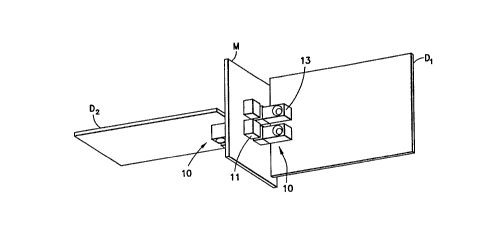
substrates, in a plurality of orientations. As seen in
Figures la and lb, interconnection systems 10 can secure
daughterboards D1, D2 to a backplane or motherboard M.
In alternate embodiments the interconnection system could
connect more or less than two daughterboards to the
motherboard and, the daughterboard(s) could be located
merely on one side of the motherboard. Daughterboards
D1, D2 can secure to motherboard M in a plurality of
i
. ~.,..~
CA 02296953 2000-O1-25 ;t,
'G
orientations. Although Figures, la and lb dez~onstrate
daughterboard D1 in a horizontal orientation and
daughterboard D2 in a vertical orientation, the
flexibility of the interconnection systems 10 allow each
5 of the daughterboards D1, D2 to secure to motherboard M
in at least four orientations. A more detailed
discussion of interconnection system 10 follows.
Interconnection system 10 includes at least two
connectors, such as a header ~11, and a receptacle 13. In
this embodiment the receptacle 13 is a right angle
receptacle. However, in alternate embodiments, any
suitable receptacle could be provided, such as when the
boards M and D1 and/or D2 are intended to be connected
parallel to each other. In addition, in an alternate
embodiment the header 11 could be located on the
daughterboard and the receptacle could be located on the
motherboard. Header 11 and receptacle 13 can secure to
daughterboards D1, D2 or motherboard M using known
techniques, which warrant no further discussion.
Preferably, interconnection system 10 uses a single ended
arrangement. for transmitting signals between
daughterboards D1, D2 and motherboard M. In this
embodiment each system 10 includes four of the headers 11
and two of the receptacles 13. However, in alternate
embodiments more or less than four headers could be
provided and more or less than two receptacles could be
provided. Referring also to Figs. lc-lf, the headers 11
and receptacle 13 are connectable to each other in four
orientations 90° offset. Sides A1-A4 can be located at
sides B1-B4 in the four positions shown. When multiple
connectors are used, some may be left .empty or
unconnected as shown in Fig. la. The connectors 11, 13
may also be arranged to mount daughterboards D1 and/or D2
;._- . ...
CA 02296953 2000-O1-25
<<w
to the mother board M in more or less than four
orientations.
Figs. 2A and 2B display one of the headers 11 prior
to mounting to motherboard M. Header 11 includes an
insulative housing 15. Housing 15 includes a base 17
surrounded by a shroud 19. Base 17 includes apertures 21
sized to receive signal contacts, or pins 23. Signal
pins 23 extend outwardly from both the mating face 17a
and the mounting face 17a of header 11. An array of
ground contacts, or pins 25, and ground shields 27
surround sides of each signal pin 23. Apertures 29 in
base 17 are sized to receive ground pins, 25 and ground
shields 27. As with signal pins 23, ground pins 25
extend outwardly from both the mating face 17a and
mounting face 17b of header 11. Ground shields 27,
however, remain within base 17. Ground pins 25 and
ground shields 27 directly contact each other in order to
provide continuity.
One of the receptacles 13 will now be described with
reference to Figures 3a, 3b, 4a-c, 5 and 6. Several
components form receptacle 13, including a rear housing
31, modules 33 and a front housing 35. However, in
alternate embodiments, more or less components can be
provided. Each component will be described in more
detail.
Rear housing 31 is generally an open structure
formed by sidewalls 36, 37; a rear wall 39; and a top
wall 41. The open interior of rear housing 31 receives
the rear portions of a series of modules 33: arranged
side-by-side. Receptacle 13 accurately rests on
daughterboard D1, D2 using alignment posts 43 extending
downwardly from sidewalls 36, 37. Alignment posts 93
CA 02296953 2000-O1-25 ;~~
' ~I
7 , tf,:
engage corresponding through holes (not shlpwn) in
daughterboard D1, D2.
Front housing 35 is also generally an open structure
formed by a mating face 45; sidewalls 47, 49; bottom wall
51; , and top wall 53. The open interior of front housing
35 receives the front portions of a series of modules 33
arranged side-by-side. Front housing 35 secures to rear
housing 31 using latch structures 55, 57 on each housing,
respectively. Front housing 35 secures to rear housing
31 after placement of modules 33 within rear housing 31.
Once assembled, receptacle 13 can mount to a
daughterboard D1, D2.
Mating face 45 of front housing 35 includes an array
of lead-ins 59. Lead-ins 59 accept corresponding signal
pins 23 and ground pins 25 from header 11. Once header
11 mates with receptacle 13, the signal and ground
contacts of receptacle 13 engage signal pins 23 and
ground pins 25 of header 11. This feature will be
described in more detail below.
Modules 33 contain the signal and ground contacts
for receptacle 13. As seen in Figures 4a-c, several
components form modules 33. Modules 33 include a wafer
61, signal contacts 63 and ground contacts 65. However,
in alternate embodiments, more components could be
provided, and/or the components need not be provided as
.uniform modules. Wafer 61 can be a block of insulative
material. As seen in Figure 4b, wafer 61 can be formed
from several pieces 61a, 61b. Alternatively, however,
wafer 61 could be formed unitarily from one piece.
As seen best in Fig. 4c, a first major surface 67 of
wafer 61 has a series of channels, grooves or apertures
..: :~eG4., r .. . . ~... .. . ,
CA 02296953 2000-O1-25
fl
8 . rr.,
68 in which signal contacts 63 and/or ground contacts 65
reside. When arranging modules 33 side-by-side, first
major surface 67 of a first module 33 can abut a second
major surface 69 of a second adjacent module 33. In
order to place modules 33 side-by-side, second major
surface 69 can be generally featureless as shown in
Figure 4b. The top surface of wafer 61 includes a
projection 71. As seen in Fig. 3A, projection 71 can
abut the front edge of rear housing 31 during, and after,
assembly. The interaction between projections 71 and the
front edge. of rear housing 31 helps align modules 33
within rear housing 31. The wafer 61 can also have a
spine 71a. The spine 71a can be located ih a groove (not
shown) in the rear housing 31.
Signal contacts 63 include a mounting end 73 for
securing to daughterboard D1, D2, a mating end 75 for
interacting with signal pins 23 of header 11, and an
intermediate portion 77. Figures 4a-c demonstrate
mounting ends 73 as having press-fit tails that engage
plated through holes (not shown) in daughterboard D1, D2.
However, other types of terminations for mounting ends 73
could be used. Typically, an over-molding process embeds
signal contacts 63 in wafer 61. However, other
techniques could be used.
Mating end 75 can have a dual beam contact to engage
signal pins 23 of header il. As seen in Figure 4b, beams
79, 81 of the dual beam contact are arranged generally
' perpendicular to each other. In this arrangement, the
bifurcation engages adjacent surfaces of signal pins 23.
Beams 79, 81 deflect upon insertion of signal'pins 23.
The movement of signal pins 23 along beams 79, 81 during
insertion provides good wiping action. In addition, the
force.imparted to signal pins 23 by the deflection of the
' , ....:.~. .: ::_
CA 02296953 2000-O1-25 i '°
y
9
beams 79, 81 provides good contact pressure orb contact
normal force.
As with signal contacts 63, ground contacts 65
include a mounting end 83 for securing to daughterboard
D1, D2, a mating end 85 for interacting with ground pins
25 of header 11, and an intermediate portion 87. Figures
4a-c demonstrate mounting ends 83 as having press-fit
tails that engage plated through holes (not shown) in
daughterboard D1, D2. However, other types of
terminations for mounting ends 83 could be used. Mating
end 85 uses a dual beam-type contact arrangement to
engage ground pins 25 of header 11. ,Mating end 85
includes a first beam 89 arranged generally perpendicular
to a second beam 91. A minor surface of first beam 89
supports the ground pin 25. As discussed above, the beam
89 provides good contact force and wipe. As seen in
Figures 4a-c, second beam 91 is bifurcated into a
stationary section 93 and a movable section 95. Upon
engagement of movable section 95 of second beam 91 with
ground pin 25, movable section 95 deflects. As with the
other contacts, the deflection provides good contact
force and wipe.
Signal contacts 63 within module 33, as with ground
contacts 65 within module 33, preferably do not maintain
the same orientation throughout module 33. Furthermore,
signal contacts 63 and ground contacts 65 in one module
33 preferably do not exhibit the same orientation as
signal contacts 63 and ground contacts 65 in all of the
other modules 33. Figure 5 helps clarify the arrangement
of the signal contacts 63 and ground contacts 65 in
modules 33.
Figure 5 provides a schematic representation of six
i _ ~.,.
CA 02296953 2000-O1-25
. . I
E»
of the modules 33 connected side-by-side with signal
contacts 63 and ground contacts 65 to form receptacle 13.
In alternate embodiments more~or less than six modules
could be used. In this embodiment the six modules 33
5 actually comprise two types of modules 33a, 33b which are
mirror images of each other. In alternate embodiments
more or less than two types of modules could be provided
and, the. modules need not be mirror images of each other.
The general L shape of the signal contacts 63 generally
10 correspond to the positions of the beams 79, 81.
Likewise, the general L shape of the ground contacts 65
generally correspond to the positions of the beams 89,
91. Two lines L1, L2, preferably passing through a
center C of receptacle 13, define four quadrants Q1, Q2,
Q3, Q4. As' discussed earlier, each signal contact 63
corresponds to a ground contact 65 to form a contact pair
97. In the arrangement shown in Figure 5, the signal
contact 63 and ground contact 65 in each contact pair 97
have the same orientation. In other words, signal
contact 63 and ground contact 65 of contact pair 97 face
the same direction. Generally speaking, the orientation
of each contact pair 97 within a quadrant remains the
same. However, the orientation of contact pairs 97 in
one quadrant differs from the orientation of contact
pairs 97 in other quadrants. Typically, contact pairs 97
in one quadrant are rotated 90° relative to contact pairs
97 in an adjacent quadrant. For example, a contact pair
97 in quadrant Q1 is rotated 90° relative to a contact
pair 97 in quadrant Q2.
Since one module 33 can have contacts 63, 65
residing in more than one quadrant, the orientation of
some contacts 63, 65 in each module 33 can differ from
the orientation of other contacts 63, 65 in the same
i .. __ ._ : . .:
CA 02296953 2000-O1-25
r
il
11 , rt;;
module 33. Typically, contact pairs 97 in a ~pdule 33
that reside in one quadrant are preferably mirrdr images
of the contact pairs 97 in the same module 33 that reside
in the other quadrant. For example, module 33a in Figure
5 has contact pairs 97 in'quadra-nts Q1 and Q4. Contact
pairs 97 in module 33a that are in quadrant Q1 are mirror
images of the contact pairs 97 in quadrant Q4. Other
arrangements are also possible. In an appropriate
situation the contacts in one quadrant could be rotated
90° to the contacts in the adjacent quadrant.
If desired, header 11 and receptacle~~l3 can utilize
additional shielding for higher speed operations. As an
example, receptacle 13 can provide additional ground
shields . or pins (not shown) along lines L1, L2.
Providing additional shielding along lines L1, L2 will
not disturb the symmetrical nature of the present
invention.
Figure 6 provides a schematic representation of an
alternative arrangement of signal contacts 63' and ground
contacts 65' in receptacle 13'. Two lines L1, L2,
preferably passing through a center C of receptacle 13',
define four quadrants Q1, Q2, Q3, Q4. As discussed
earlier, each signal contact 63' corresponds to a ground
contact 65' to form a contact pair 97'. In the
arrangement shown in Figure 6, each signal contact 63'
has an opposite orientation from its respective ground
contact 65' in each contact pair 97'. In other words,
signal contact 63' faces ground contact 65' in contact
pair 97'.
Aside from the opposite orientation of . signal
w~.,yt ~ ~:~:.,.
CA 02296953 2000-O1-25
t
S
12
contact 63' from ground contact 65' in each contact pair
97', the remaining features described with reference to
Figure 5 above still apply. That is, all contacts pairs
97' within a quadrant have the same orientation. Also,
the orientation of contact pairs 97' in one quadrant
differs from the orientation of contact pairs 97' in
other quadrants. Typically, contact pairs 97' in one
quadrant are rotated 90° relative to contact pairs 97' in
an adjacent quadrant. Finally, contacts 63', 65'
residing in module 33a' in one quadrant have a different
orientation than the other contacts 63', 65' in module
33b'. Typically, contact pairs 97a' in module 33' that
reside in one quadrant are rotated 90° relative to
contact pairs 97b' in module 33a' that reside in the
other quadrant.
In either arrangement shown in Figs. 5 or 6,
contacts 63, 65; 63', 65' in receptacle 13; 13' are
. symmetric about lines L1, L2. Since lines L1, L2
preferably pass through center C of receptacle 13: 13',
contacts 63, 65; 63', 65' in receptacle 13~ 13' are
symmetric about center C of receptacle 13; 13'. As a
result, receptacle 13; 13' can mate with header 11 in at
least four orientations. When compared to conventional
"polarized" connectors, the present invention provides
flexibility to the design of the electrical system.
Referring now to Fig. 7 a schematic view, similar to
Figs. 5 and 6, of an alternate embodiment of the
receptacle 13" is shown. In this embodiment the
receptacle 13" comprises an array of 64 contact pairs 97
arranged in four quadrants Q1, Q2, Q3, Q4 with' 16 pairs
in each quadrant. The receptacle 13" is comprised of
eight modules 33" of the modules types 33a", 33b". Each
modules 33" has eight of the pairs 97 of the contacts 63,
i
1 CA 02296953 2000-O1-25 . ;;
i
13 1
65; four arranged in one quadrant in one dire~tion as
pairs 97a and four arranged in another quadrant in a
second 90° offset direction as pairs 97b. Any suitable
number of contact pairs could be provided in each module.
Referring now to Figs. 8 and 9 another alternate
embodiment of the present invention is shown. In this
embodiment the receptacle 100 generally comprises a
housing 102 and a module assembly 104 connected to the
housing 102. The housing 102 generally comprises a first
housing member 106 and a second housing member 108. The
first and second housing members 106, 108 are preferably
comprised of a dielectric material, such as a molded
plastic or polymer material. The first housing 106
includes a top 110, a back 112, two sides 114, a
generally open front 116, a generally open bottom 118,
and a receiving area 120. The top 110 includes module
mounting holes 122. The back 112 includes module
mounting holes 124. The front 116 includes extensions
126 from the sides 114 for insertion into and connection
with the second housing member 108. The second housing
member 108 includes apertures or lead-ins 128 through a
front face 130 for insertion of the front ends of the
mating connector's male pins into the connector 100.
The module assembly 104, in this embodiment,
generally comprises six contact modules 132. In alternate
embodiments more or less than six contact modules could
be provided. In this embodiment the contact modules 132
comprise two sets of two types of contact modules 132a,
132b which are preferably mirror images of each other.
Referring also to Fig. 10, each contact module 132
generally comprises a one-piece frame 190, signal
contacts 142, and ground contacts 144. The frame 140 is
preferably comprised of dielectric material, such as
CA 02296953 2000-O1-25
_ ..
J
14 is
molded plastic or polymer. The frame 140 comprises a top
side 146, a bottom side 148, a rear side 150,~a front
side 152, and two lateral sides 154, 156. The top side
146 includes a latch 158. The latch 158 is inserted into
one of the module mounting holes 122 to connect the
contact module 132 to the first housing member 106. The
rear side 150 also includes a projection 160. The
projection 160 is inserted into one of the module
mounting holes 124 to connect the module 132 to the first
housing member 106. The frame 190 includes channels 162
along at least one of the sides 154 for receiving
portions of the ground contacts 149. The frame 140 could
also have channels for receiving portions of the signal
contacts 142. However, the frame 140 is preferably over-
molded onto portions of the signal' contacts 192.
Alternatively, or additionally, the frame 140 could be
over-molded onto portions of the ground contacts 144.
The front side 152 of the frame 140 includes pockets 164
and receiving areas 165.
In this embodiment each contact module has six of
the signal contacts 142 three as a first type 142a of
signal contacts and three as a second type 142b of signal
contacts. The signal contacts 142 each have a first end
166, a middle section 168, and a second end 170. The
first ends 166 have through-hole solder tails, but any
suitable first ends could be provided, such' as surface
mount solder tails. The middle sections 168 all have
right turn shapes, but with different lengths or
dimensions to allow the signal contacts to be aligned in
a row or common plane. The second ends 170 each comprise
two deflectable arms 172, 174 oriented 90° offset from
each other. The arms 172, 174 in the first type of
signal contact 142a are orientated as mirror images of
i
CA 02296953 2000-O1-25
It
15 rp:.
the arms 172, 174 in the second type of signal~icontacts
142b. In alternate embodiments other t~ipes or
orientations of the second ends could be provided.
The ground contacts 144 for each module 132 can be
provided as a single one-piece member or multiple members
as shown. Each ground contact 144 includes a first end
176, a middle section 178, and a second end 180. The
first ends 176 have press fit tails. However,
any suitable type of first ends could be provided, such
as surface mount solder tails. The middle sections 178
generally comprise first sections 182 and second sections
184. The first sections 182 are located in the slots 162
of the frame 140 to fixedly connect the ground contacts
144 to the frame 140. The second sections 184 extend
along the side surface 154 of the frame 140. The middle
sections 178 have a general right turn shape such that
the two ends 176, 180 are at a general right angle to
each other. However, any suitable shape of the middle
sections could be provided.
Referring also to Fig. 11, the second ends 180
include three different types of second ends 180a, 180b,
180c. The first type of second end 180a has a slot 186a
at a corner with a top arm 188a and a side arm 190a on
opposite sides of the slot 186a. Two deflectable
projections 192a, 199a extend from the arms 188a, 190a.
The second type of second end 180b is generally a mirror
image of the first type of second end 180a. The second
type of second end 180b has a slot 186b at a corner with
a side arm 190b and a bottom arm 196b. Two deflectable
projections 192b, 194b extend from the arms 196b, 190b.
The third type of end 180c has two slots 186c1, 186c2 at
two corners with a top arm 188c, a bottom arm 196c and a
side arm 190c. Two deflectable projections 192c, 199c
i _
CA 02296.953 2000-O1-25
,S,
. . i~
16 ~ r:
r; ..
extend into the first slot 186c, and two def~Q.ectable
projections 192c, 194c extend into the second sld~t 186c2.
The side arm 190c also includes a third slot 198.
However, in alternate embodiments, any suitable types)
, of second ends could be provided.
Referring back to Fig. 9, when the module assembly
109 is assembled the ground contacts 144 combine to
effectively surround the signal contacts to form an
electromagnetic shielding for the signal contacts.
. While the present invention has been described in
connection with the preferred embodiments of the various
figures, it is to be understood that bother similar
embodiments' may be used or modifications and additions
may be made to the described embodiment for performing
the same function of the present invention without
deviating therefrom. Therefore, the present invention
should not be limited to any single embodiment, but
rather construed in breadth and scope in accordance with
the recitation of the appended claims.