Note: Descriptions are shown in the official language in which they were submitted.
CA 02297037 2000-O1-19
WO 99/05726 PCT/US98/15362
SEMICONDUCTOR WITH TUNNEL HOLE CONTACT SOURCES
This invention was made with U.S. Government support
under Contract DAAH04-96-1-033 of Army Research Office, under
Contract MDA972-94-1-004 of DARPA Center of Optoelectronics
Science and Technology, and under Grant SBCUTC-97-0080 of
National Science Foundation. The U.S. Government has certain
rights in this invention.
FIELD OF THE INVENTION
This invention relates to semiconductor devices and
methods. The invention has particularly advantageous
application to III-V semiconductor light emitting devices,
including semiconductor lasers and semiconductor light
emitting diodes (LEDs).
BACKGROUND OF THE INVENTION
In many semiconductor devices, there is a substantial
volume of both n-type semiconductor material (that is,
semiconductor doped with donor impurities so that electrons
are majority carriers) and p-type semiconductor material (that
is, semiconductor doped with acceptor impurities so that holes
[shortage of valence electrons] are majority carriers). In
III-V semiconductor light emitting devices (e.g. lasers or
LEDs), an active region can be disposed between n-type and p-
type semiconductor regions. Upon application of an electrical
potential, holes entering the active region from the p-type
semiconductor material recombine with electrons entering the
active region from the n-type semiconductor material, and
photons are emitted.
In several respects, p-type material is more difficult to
work with than n-type material, and tends to be operationally
inferior to corresponding n-type material with regard to
CA 02297037 2000-O1-19
WO 99/05726 PCT/US98/I5362
2
carrier mobility and overall electrical efficiency.
Accordingly, it is often desirable to favor the use of n-type
semiconductor material in the fabrication of semiconductor
devices such as III-V light emitting devices. However, even
though the substrate and a fractional majority of the
semiconductor volume in such devices may be n-type
semiconductor or undoped semiconductor, a substantial amount
of p-type material is generally considered necessary as a
source of hole current in various semiconductor devices. As
described further hereinbelow, the disadvantages of employing
p-type material in certain devices is even more pronounced
when currents must travel laterally through p-type layers in
planar devices.
It is among the objects of the present invention to
improve semiconductor devices and methods by reducing the
amount of p-type material that is needed in certain
applications.
SUMMARY OF THE INVENTION
The present invention is directed to semiconductor
devices and methods in which the amount of p-type material can
be minimized, with attendant advantages in electrical,
thermal, and optical performance, and in fabrication.
A form of the invention is directed to a generally planar
semiconductor device wherein a layer of p-type semiconductor
material is disposed over (that is, directly on or with one or
more intervening layers) a layer of n-type semiconductor
material, and an electric potential is coupled between the p-
type layer and the n-type layer, and wherein current in the
device that is lateral to the plane of the layers is coupled
into the p-type layer. The improvement in this form of the
invention comprises a tunnel junction adjacent the p-type
layer for converting the lateral current into hole current.
In an embodiment of this form of the invention, the tunnel
junction is an n+/p+ junction oriented with the p+ portion
thereof adjacent said p-type layer. [The "+" notation
conventionally means "heavily doped", and, for purposes
CA 02297037 2000-O1-19
WO 99/05726 PCT/US98/15362
3
hereof, is generally donor impurity concentration of at least
about 1018/cm3 for n+, and acceptor impurity concentration of
at least about 1019/cm' for p+.] The lateral current can be
electron current in the n+ layer and/or electron current in a
further layer of n-type material disposed over the tunnel
junction.
Tunneling in GaAs, at an n+/p+ junction, is well known
(see, for example, N. Holonyak, Jr. and I.A. Lesk, Proc. IRE
48, 1405, 1960), and is generally of interest for its negative
resistance. Tunneling in GaAs can be enhanced with an InGaAs
transition region (see, for example, T.A. Richard, E.I. Chen,
A.R. Sugg. G.E. Hofler, and N. Holonyak, Jr., Appl. Phys.
Lett. 63, 3613, 1993), and besides fts negative resistance
behavior, can be used in reverse bias as a form of "ohmic"
contact. This allows, for example, the reversal of the doping
sequence of an AIXGaI-xAs-GaAs quantum well heterostructure
laser (n ~ p to p -~ n) grown on an n-type GaAs substrate (see,
for example, A.R. Sugg, E.I. Chen, T.A. Richard, S.A.
Maranowski, and N. Holonyak, Jr., Appl. Phys. Lett. 62, 2510
(1993). A form of the present invention is directed to a
semiconductor light emitting device (e. g. a semiconductor
laser or a semiconductor light emitting diode) which comprises
the following: a semiconductor active region disposed between
first and second semiconductor layers, the first semiconductor
layer being p-type, and the second semiconductor layer being
n-type; tunnel junction means disposed over the first
semiconductor layer; and means for coupling electric potential
between the tunnel junction means and the second semiconductor
layer; and means for causing lateral electron flow into the
tunnel junction means.
A tunnel contact junction can be used in a light emitting
semiconductor device as a hole source and makes possible
lateral bias currents (electron current) to drive a quantum
well heterostructure (QWH) laser without the compromise of the
low mobility and large resistive voltage drop of lateral
conduction in thin p-type layers. This is particularly
valuable in QWH laser structures employing upper and/or lower
CA 02297037 2000-O1-19
WO 99/05726 PCT/US98115362
4
native oxide confining layers (see, for example, M.
Dallesasse, N. Holonyak Jr., A.R. Sugg, T.A. Richard, and N.
E1 Zein, Appl. Phys. Lett 57 2844, 1990; A.R. Sugg, E.I. Chen,
T.A. Richard, N. Holonyak, Jr., and K.C. Hsieh, Appl. Phys.
Lett. 62, 1259, 1993) that require lateral bias currents (see,
for example, P.W. Evans, N. Holonyak, Jr., S.A. Maranowski,
M.J. Ries, and E.I. Chen, Appl. Phys. Lett. 67, 3168, 1995),
or in devices such as a vertical cavity surface emitting laser
(VCSEL) where lateral hole currents have been employed (see,
for example, D.L. Huffker, D.G. Deppe, and K. Kumar, Appl.
Phys. Lett. 65, 97, 1994). Hole conduction along a layer
introduces a large device series resistance, because of the
low hole mobility in GaAs, and increases threshold voltages
and device heating. A tunnel contact junction on the p side
of an oxide confined QWH can be used to replace lateral hole
excitation currents. The hole injection is supported by a
lateral electron current, thus providing lower voltage drop
and less series resistance. An objective hereof is to
minimize the amount of p-type material and, to the extent
possible, employ only n-type layers (electron conduction) to
carry the device current. In addition to electrical and
thermal performance advantages from reducing the amount of
lossier p-type material, optical advantage can also accrue
since p-type material of the same conductance as n-type
material will generally be more absorptive of the light being
generated in semiconductor light emitting devices.
Conversely, since the tunnel contact junction is highly doped,
it should be kept relatively thin to avoid undue light
absorption.
Further features and advantages of the invention will
become more readily apparent from the following detailed
description when taken in conjunction with the accompanying
drawings.
BRIEF DESCRIPTION OF THE DRAWINGS
Figure 1 shows current density at threshold (Jth) vs.
inverse cavity length (1/L) for the broad area quantum well
CA 02297037 2000-O1-19
WO 99/05726 PCT/US98/15362
heterostructure (QWH) lasers in accordance with an embodiment
hereof, with reverse-biased tunnel junction contacts contained
in the p-type cladding at different distances, z, from the
quantum well (QW) and waveguide active region as shown in the
inset of the Figure.
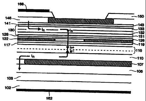
Figures 2 and 3 are cross-sectional diagrams (not to
scale) of an edge-emitting semiconductor laser device in
accordance with an embodiment of the invention and made in
accordance with a technique of the invention, with Figure 3
being a more detailed diagram and Figure 2 being simplified to
facilitate understanding of operation.
Figure 4 is a scanning electron microscope image (cross
section) of the tunnel contact QWH laser of the diagram of
Figures 2 and 3. Lateral oxidation (middle "Ox" layer)
defines a ~3.5 Nm current aperture and, with the top and
bottom oxide layers, forces lateral electron current flow, In,
as shown in Figures 2 and 3. The "Ox" marker arrows are
slanted to point along the layers in the direction of
oxidation. The tunnel contact junction (n+/p+) is just below
the top oxide cladding and just above the current aperture.
Figure 5 shows current density at threshold (Jth) vs.
inverse cavity length (1/L) for tunnel contact junction QWH
lasers hereof: (a) broad area (width = 150 um) laser, (b)
tunnel contact laser with top oxide cladding and 3.5 Nm oxide-
defined current aperture, and (c) tunnel contact laser with
top and bottom oxide claddings and 3.8 Nm oxide-defined
current aperture.
Figure 6 shows current-voltage (I-V) characteristics of
tunnel contact junction QWH lasers hereof: (a) broad area
(150 um) laser, (b) laser with top oxide cladding and 3.8 Nm
current aperture, and (c) laser with top and bottom oxide
cladding and 3.5 um current aperture. The series resistances
of the three lasers increase from (a) R8~10 ohm, to (b) ~15, to
(c) only ~20.
Figures 7 and 8 are cross-sectional diagrams (not to
scale) of vertical cavity surface emitting laser (VCSEL)
devices in accordance with an embodiment of the invention and
CA 02297037 2000-O1-19
WO 99/05726 PCT/US98/15362
6
made in accordance with a technique of the invention, with
Figure 8 being a more detailed diagram and Figure 7 being
simplified to facilitate understanding of operation.
Figure 9 is an optical microscope image (top-view) of a
partially fabricated tunnel contact junction VCSEL hereof
after oxidation. The aperture is formed by "wet" oxidation
laterally -5 arm from a -20 Nm-diameter disk edge creating a
~10 Nm opening (unlabeled horizontal arrow). The DBR oxidizes
laterally from the trench edge (double arrow) and proceeds ~22
arm (terminating at the single arrow), which oxidizes the DBR
completely underneath the aperture.
Figure 10 shows the (a) light vs. current (L-I) and (b)
current vs. voltage (I-V) characteristics for the tunnel
contact junction VCSEL of Figures 7-9. The lasing threshold
is 0.55 mA and the external differential quantum efficiency
~35%. The diode turns on at ~1V.
Figure 11 shows the light vs. current characteristics
(inset) for a tunnel contact junction VCSEL (as in Figure 7-
9). The spectrum is narrow (45 1~, 0.5 mA) due to amplified
spontaneous emission, with current threshold at 1 mA. Laser
operation is centered at the wavelength 990 nm.
Figure 12 is a cross-sectional diagram (not to scale) of
a light-emitting diode in accordance with an embodiment of the
invention and which can be made in accordance with a technique
of the invention.
Figure 13 shows an example of a variation of the Figure
12 device.
DETAILED DESCRIPTION
In an early phase of work on the invention, crystals were
grown to investigate first the effect of introducing a heavily
doped region, a tunnel contact junction, close to the
waveguide active region of a standard quantum well
heterostructure (QWH) laser. The crystals were grown by
metalorganic chemical vapor deposition (MOCVD) on n-type
substrates with Si as the n-type dopant and C as the p-type
dopant. [For background regarding MOCVD, see, for example,
CA 02297037 2000-O1-19
WO 99/05726 PCT/US98/15362
7
R.D. Dupuis, L.A. Moudy, and P.D. Dapkus, in Proceedings of
the International Symposium on GaAs and Related Compounds,
edited by C.M. Wolfe, Institute of Physics, London, 1979, pp.
1-9. See also, M.J. Ludowise, J. Appl. Phys. 58, R31, 1985.]
First, an n+ GaAs buffer layer and then a 0.8 pm n-type
Alo.esGa°.~sAs layer were grown. An undoped GaAs waveguide region
(2400 ~) with an Inl_yGayAs (-980 nm, y - 0.2) quantum well (QW)
in the center was grown next. Then, 0.8 arm of upper (top)
cladding crystal consisting mainly of Al°.aSGao.lSAs, was grown,
with a tunnel junction (TJ) inserted at varying distances from
the waveguide (0.2, 0.4, and 0.8 Nm, see insert of Fig. 1).
The QWH crystal just below the TJ was p-type, and above was n-
type. From bottom to top the TJ included 300 ~ of p+ (~ 102°
cm') GaAs, -100 ~ of n+ ( >lOl9cm 3) In°_1°Ga°,soAs, and -
300 ~ of
n+ (-.1019 cm 3) GaAs. Finally, the crystal was capped with 1500
A of n+ GaAs. The cladding layers were grown at a temperature
of 740°C, the WG at 640°C, and the TJ at 570°C for the n+
region and 540°C for the p+ region, all at a VIII ratio ~40.
Broad area lasers were fabricated, first by defining 150
Nm stripes in Si3N4 deposited on the QWH crystal surface and'
then by evaporating and alloying (375°C, 10 s) Ge/Au/Ni/Au on
the epitaxial-layer side and Ge/Au on the substrate side. The
crystals were cleaved, diced, and probed under pulsed (2 Ns,
1% duty cycle) operation (300 K). The current densities at
threshold (Jth) vs. inverse cavity length (1/L) were measured
and shown in Figure 1. As was expected, if the TJ was brought
closer to the WG and QW, the threshold current density
increased due to increased absorption losses and asymmetry in
the waveguide structure. A TJ as close as 0.2 um to the
waveguide in a standard QWH laser resulted in only a two-fold
increase in the threshold current density compared to a TJ
contact located as far away as 0.8 um. The TJ contact caused
only a relatively small compromise in current thresholds.
Other crystals were grown that could be processed to give
buried-oxide apertures and oxide claddings. Reference can be
made to Figures 2 and 3, with Figure 3 showing the greater
detail and Figure 2 being simplified to facilitate
CA 02297037 2000-O1-19
WO 99/05726 PCT/US98/15362
8
illustration of operation. The substrate layer and buffer
layer (102 and 103, respectively, in Figure 3) can be the n-
type GaAs layers as described above. The n-type bottom
confining layers included 3000 i4 of Alo.6Gao.4As ( layer 105 ) ,
1500 A of A1o.98Gao.o2As ( layer 107 - for the bottom oxide
cladding layer ) , and 2000 ~ of Alo,6Gao.4As ( layer 110 ) . The
undoped waveguide (WG) region (115) was grown with an InyGal_yAs
QW 0980 nm, y -0.2) sandwiched between 1200 ~ of GaAs on
either side. The p-type layer for later conversion into a
buried oxide aperture was grown over the active region and
consisted of 600 ~ of A1o.95Gao_pSAs ( layer 122 - for subsequent
conversion) with 100 1~ of Alo.6Gao.4As ( layers 119 and 126 ) and
Alo.3Gao.~As ( layers 117 and 128 ) on each side. The TJ for hole
injection was grown next and included -100 ~r of p+ GaAs (layer
131 ) , -100 ~r of n+ Ino.loGao.9oAs ( layer 132 ) , and -100 1~ of n+
GaAs (layer 133). The n-type upper (top) confining layers
followed and included -300 14 of Alo.3Gao.~As ( layer 141 ) , --300 ~1
of Alo.6Gao,4As ( layer 143 ) , and 2000, ~r of A1o.85Gao.15As ( layer 146
- for the top oxide cladding). The crystal was capped with
1500 ~r of n+ GaAs (layer 150).
For the oxide-defined QWH lasers of Figures 2 and 3,
laser fabrication again begins with the deposition of Si3N4
that is then patterned into two ~4 Nm wide stripes ~11 pm
apart (center-to-center). With the aid of photolighography
and wet etching ( HZS04: H20z: HzO, 1: 8 : 80 ) the dif ferent layers to
be laterally oxidized are exposed on the outside edges and
between the Si3N4 stripes. One outside edge is etched just
past the aperture depth, while the other is etched past the
bottom oxide cladding layer. Between the stripes only the
1500 A GaAs cap is removed (etched), exposing the top
Alo,esGao.~sAs for oxidation. The crystal is then oxidized
(430°C, 35 mim) in an open tube furnace supplied with H20 vapor
in a NZ carrier gas. [See, for example, M. Dallesasse, N.
Holonyak Jr., A.R. Sugg, T.A. Richard, and N. E1-Zein, Appl.
Phys. Lett. 57, 2844 (1990).]
A scanning electron microscope (SEM) image of the device
cross section after oxidation is shown in Figure 4. The
CA 02297037 2000-O1-19
WO 99/05726 PCT/US98/15362
9
arrows in Figure 4 are slanted to show the direction of
oxidation along the layers. The aperture layer oxidizes
laterally from both outside edges forming a -3.5 um current
aperture (see, for example, S.A. Maranowski, A.R. Sugg, E.I.
Chen, and N. Holonyak, Jr., Appl. Phys. Lett. 63, 1660, 1993)
just above the active region (WG + QW). The lower cladding
oxidizes laterally from only one edge (right side in Figure
4), while between the edges of the top Si3N4 defining stripes
the Alo,esGao.~sAs layer ( 146 ) oxidizes downward from the surface
and slightly under the Si3N4 stripes and capping layer. This
oxidation pattern provides an oxide-defined current aperture
and the top and bottom oxide cladding and results in a device
that depends upon lateral current for laser operation. Only
lateral electron currents (In, Figures 2 and 3) in high
mobility n-type layers are required for excitation. This
includes the current driving the TJ that then supplies holes
for the small amount of p-type crystal just above the active
region. For the sake of comparison, other devices were
fabricated similarly, but without the bottom oxide cladding so
that only the behavior of the TJ with its lateral electron
bias current could be addressed.
Fabrication of the oxide-defined lasers was completed by
first removing the two Si3N4 stripes and then covering the
capping layer and the space in between with photoresist.
Next, 1500 A of SiOz was electron-beam evaporated onto the
crystal, and the Si02 above the photoresist was lifted off.
This filled in the mesa on the shallow side (above the TJ) and
prevents the device from being shorted out. The Si3N4 was
removed and Ge/Au/Ni/Au was evaporated on the epitaxial side
of the crystal over the mesas and shallower etched edge, and
Ge/Au was evaporated on the substrate side. Both contacts
(168, 162) were alloyed at 375°C for 10 s. Diodes were
cleaved from the wafer, diced and either probed for pulsed
operation or mounted (epitaxial-layer side) on In-coated
copper heat sinks for continuous (cw) operation.
Figure 5 shows the QWH laser threshold current density Jtn
vs. 1/L for three sets of devices under pulsed conditions at
CA 02297037 2000-O1-19
WO 99/OS726 PCT/US98/15362
room temperature. All the devices were from the same crystal
where (a) represents 150 Nm wide broad area lasers (non-
oxidized), (b) are oxide-aperture lasers (width = 3.8 Nm) with
just the upper cladding oxidized, and (c) are oxide-aperture
lasers with both claddings oxidized. The performance (low
threshold) of the broad area lasers shows that the crystal was
of good quality. By creating an oxide-defined current
aperture and oxidizing the upper cladding layer (b), the
threshold currents were increased by only 100 A/cm2 compared
to (a). This indicates that the lateral electron current and
TJ are effective in providing hole injection without the
penalty of much additional series resistance, voltage drop,
heating, or increase in threshold current. Also, by adding
the lower oxide cladding, the threshold currents were
increased further, but only by a relatively small amount.
To investigate the series resistance that is added to
these devices by introducing oxide claddings and an oxide-
defined current and thus forcing lateral bias currents, the
current-voltage (I-V) characteristics of (a) a 150 pm broad
area laser, (b) a QWH laser with oxide-defined aperture and
top oxide cladding, and (c) the same as (b) but with top and
bottom oxide claddings, were compared and the results shown in
Figure 6. The broad area laser (and no lateral current)
turned on at 1.0 V and had a series resistance of R ~ 10 St.
The diode of (b) turned on slightly higher at 1.2 V and had a
series resistance of only ~15 S2 (in spite of its smaller
width), while (c) had about the same turn-on voltage and only
a slightly larger series resistance of R8 ~ 20 S2. This showed
that the lateral currents added only a small amount of series
resistance and additional voltage drop, and that the TJ is
efficient in lateral current operation (i.e., in effecting
current spreading).
The diode whose I-V characteristic is shown in Figure
6(c) operated cw with a threshold current of 10 mA (data not
shown), and output power of 16 mW (without damaging the
device). The total external differential quantum efficiency
was ~t - 59%, and the field was transverse electric (TE)
CA 02297037 2000-O1-19
WO 99/05726 PCT/US98/15362
11
polarized. The measured near field width at half-maximum was
3.4 pm (I1 mA) which agreed with the aperture width. A
lateral far-field pattern of this diode was single-lobed with
a full angle at half-power of 21°, in the crystal plane and
42° in the vertical direction.
It is seen from the foregoing that by employing p+/n+
tunnel junctions (GaAs-InGaAs in these examples) to contact
(internally) the p region of an AlGaAs-GaAs-InGaAs QWH laser,
one can enclose a QWH laser with buried oxide layers and
successfully introduce the excitation current laterally via
high mobility n-layer electron conduction (not low mobility
hole conduction). An achieved objective is the reduction of
the p-type material of a QHW laser and the use of electron
current as the lateral current, internally and at the
terminals, to excite the device without the relatively large
penalty in increased resistance that one would encounter in
the p-type material of a conventional QWH laser diode. As
seen, if the TJ is grown closer to the QW, absorption losses
increase the threshold current, but to an acceptable extent.
A vertical cavity surface emitting laser in accordance
with an embodiment of the invention is shown in Figures 7 and
8, with Figure 8 showing the greater detail and Figure 7 being
simplified to facilitate understanding of operation. As
before, the crystals employed for exemplary devices were grown
by metalorganic chemical vapor deposition (MOCVD) on n-type
GaAs substrates {layer 802) and buffers (layer 804). The
crystal growth began with a 6.5 period stack of n-type
A1o.98Gao.oZAs/GaAs ( layers 812 and 815 respectively) , each to be
-ll/4 thickness after oxidation (including buffer layers 813 of
Alo_~SGaa.ZSAs ) , followed by a 1l/4 layer ( 816 ) of n-type
Alo.esGao.lSAs. The n-type JL/4 thickness GaAs (uppermost layer
815 ) and A1o.85Gao.15As layer ( 816 ) are for the bottom-side
lateral electron conduction. Next, an undoped 7l thickness
cavity was grown. The active region cavity (830) was formed
with two -70 ~ InGaAs quantum wells separated by --50 ~ of GaAs
sandwiched between 500 ~ of GaAs and 860 ~1 of Alo.SGao.SAs on
each side. Then, a p-type A1o.94Gao.o6As upper confining layer
CA 02297037 2000-O1-19
WO 99/05726 PCT/US98/15362
12
(840) was grown of ~./4 thickness, (with buffer layers 843 and
845 of p-type Alo_TSGao.zSAs ) that later was partially oxidized to
form the current aperture. The structure described so far was
capped with a Jl/4 thickness p+/n+ GaAs tunnel contact junction
860 that allows lateral electron current to supply hole
injection, via the p-type aperture, into the active region.
The tunnel junction in this example included ~ 150 ~ of p+
GaAs (layer 862}, and ~ 550 ~ of n+ GaAs (layer 863).
Fabrication proceeded with photolithography and wet
etching ( HzSOa: HZO2: HZO, 1: 8 : 40 ) to form a ~46 um wide trench
exposing the bottom DBR for oxidation (double arrow, "Ox" in
Figure 9). A second photolithography process and a shallower
wet etching step defined a ~20 pm diameter disk ~8 Nm from the
trench edge, exposing just the A1o.94Gao.o6As aperture layer
(840). The sample was then oxidized in an open tube furnace
supplied with H20 vapor in a NZ carrier gas for a total of 45
min at 430°C (see, for example, J.M. Dallesasse, N. Holonyak,
Jr., A.R. Sugg, T.A. Richard, and N. el-Zein, Appl. Phys.
Lett. 57, 2844, 1990}.
Figure 9 is an optical microscope image (top-view) of the
described tunnel contact junction VCSEL just after crystal
oxidation. The aperture layer oxidizes laterally ~5 um from
the edge of the -20 ~cm disk defining a current aperture of ~10
pm diameter (unlabeled horizontal arrow in Figure 9). The
lower DBR oxidizes from the trench edge (double arrow)
underneath the aperture for a total distance of ~22 um. The
upper arrow shows where the lower DBR oxidation ends. The
oxidation defines the oxide-aperture and the AlxOy/GaAs lower
DBR.
After the oxidation procedure the 20 um diameter disks
were covered with photoresist, and 1500 A of SiOz was electron-
beam evaporated onto the crystal. The photoresist was lifted
off leaving a SiOz coating (870) to prevent shorting by
subsequent metallizations. Ti/Au was evaporated for the top
metal contact (872) with a ~12 Nm diameter opening centered on
the ~i0 Nm laser aperture. The crystal was then lapped and
polished to 125 um thickness. Ge/Au was evaporated on the
CA 02297037 2000-O1-19
WO 99105726 PCT/US98/15362
13
substrate and was alloyed at 375°C for 10 s to obtain contact
875. Then, five periods of Si02/Si (layers 881, 883,
respectively), each layer of X1/4 thickness, were electron-beam
evaporated for the upper DBR. Diodes were mounted oriented
expitaxial-layer side upward on In-coated copper heat sinks
for continuous (cw) laser operation at room temperature (300
K).
The deposition of the upper DBR, with alternating layers
881 and 883 of Si02 and Si, completed the structure forming a
compact high Q cavity in the vertical direction (normal to the
substrate). Current flows into the substrate by wrapping
around the lower AlxOy/GaAs DBR. From the top side of the
VCSEL, lateral electron currents drive the tunnel contact
junction (TJ n+/p+), which in turn supplies holes (h+) to
forward bias the small amount of p-type crystal at and above
the active region. The tunnel contact junction eliminates the
need for lateral hole conduction, and the amount of p-type
material and hole conduction are minimized. All lateral
conduction involves electron currents to thus lower device
resistance, voltage drop, and heating.
Figure 10 shows (a) the light vs. current (L-I) behavior
and~(b) the current vs. voltage (I-V) characteristic for the
described tunnel contact junction VCSEL. All measurements
were at room temperature under cw conditions. The L-I curve
has a steep slope (see P.W. Evans, N. Holonyak, Jr., S.A.
Maranowski, M.J. Ries, and E.I. Chen, Appl. Phys. Lett. 67,
3168, 1995) before threshold that is characteristic of
amplified spontaneous emission (ASE). The threshold current
was 0.55 mA (Jth ~ 700 A/cmz) and the emission wavelength was
--986 nm. The external differential quantum efficiency was
~35% while the total power efficiency (wall plug) was ~12% at
1 mA. The diode turned on sharply at ~1 V. The tunnel
junction contact of the device was not optimized since other
comparison diodes fabricated from similarly designed crystals
exhibited sharper I-V characteristics with series resistances
of -100 St, but did not lase because of detuned cavities. This
shows that a VCSEL can operate with a tunnel contact junction
CA 02297037 2000-O1-19
WO 99/05726 PCT/US98/15362
14
that provides holes via lateral electron current without
excessive voltage drop.
Figure 11 shows the spectra and L-I curve (inset) for a
further tunnel contact junction VCSEL fabricated in a similar
manner. This device also had a region of amplified
spontaneous emission (ASE) and steep L-I slope before
threshold at 1 mA. The spectra show that the ASE is narrow
(45 ~) and that some ringing occurs, possibly due to lateral
disk modes (see H. Deng. Q. Deng, and D.G. Deppe, Appl. Phys.
Lett. 69, 3120, 1996). At 1.5 mA the spectra were narrow -1
and centered at 990 nm. This wavelength difference compared
to the diode of Figure 10 may be related to the higher
threshold (slight de-tuning), and lower (- 17~) external
differential quantum efficiency. This further device had a
maximum power output of 0.55 mW.
The tunnel contact junction allows for the reduction of
p-type material in the VCSEL structure and provides hole
injection into the active region via lateral electron
currents. It will be understood that tunnel junctions can be
used not only in the previously described hybrid VCSELs and
edge emitters with native-oxide-based layers but also, for
example, in other forms of VCSELs, edge-emitting lasers, and
light emitting diodes that require lateral currents for
excitation or reduction of p-type material.
Referring to Figure 12, there is shown a light emitting
diode (LED) in accordance with an embodiment of the invention.
An n-type substrate 1205 has an n-type confining layer 1215
disposed thereon. The substrate 1205 may be, for example,
GaAs or GaP, and the lower confining layer 1215 may be, for
example, n-type AlGaAs. It will be understood herein, and
elsewhere, that additional layers, for example buffer layers
may be present. An active region is represented at 1230, and,
as elsewhere, will be selected to obtain the desired light
wavelength. As one example, the active region may be bulk
AlGaInP or may include one or more quantum wells of GaAs or
InGaP between layers of AlGaInP. An upper confining layer
1240 is a p-type layer, for example a layer of p-type AlGaAs
CA 02297037 2000-O1-19
WO 99/05'726 PCT/US98/15362
or AlInP. Above the p-type upper confining layer 1240 is the
p+ layer 1252 and an n+ layer 1254. Here, as elsewhere, both
of these layers may be heavily doped GaAs or, for example, the
n+ portion may include two n+ layers, such as a layer of n+
InGaAs with n+ GaAs thereon. The tunnel junction is labelled
at 1250. Metal contacts 1261 and 1265, which may be, for
example Ti/Au or Ge/Au, are respectively applied to the top
and bottom of the light emitting diode. A positive potential
can be applied via the contacts, as shown. In the embodiment
Figure 12, the top electrode is a ring electrode, and a
substantial portion of the top of the device, inside the ring,
is an aperture through which the generated light can be
emitted. Alternative electrode configurations can be used,
for example as shown in Figure 13 wherein a central (e. g.
circular) contact 1361 is used, and the light from the LED is
emitted outside the region of the electrode. In either case,
there will be lateral current flow as current travels from the
contacts) and eventually into an active region having greater
area (in the plane of the layers) than the area the contacts)
cover. In prior art devices, where this traversal is through
p-type material, it is generally necessary to have the p-type
material be of sufficient thickness to carry the lateral
current without undue loss, since the p-type material has
relatively lower mobility hole conduction. As previously set
forth, an advantageous feature of the present invention is
that the p-type layer can be made substantially thinner (with
attendant reduction in electrical and optical losses), and n-
type semiconductor material can be used to carry electron
current in more efficient manner, and laterally where
necessary, with the tunnel junction operating to convert
electron current to hole current.