Note: Descriptions are shown in the official language in which they were submitted.
CA 02297058 2004-O1-27
- 1
ELECTRODE MEANS WITH AND WITHOUT THE FUNCTIONAL ELEMENT
AND AN ELECTRODE DEVICE FORMED OF ELECTRODE MEANS WITH
FUNCTIONAL ELEMENTS AND USES THEREOF
The invention concerns an electrode means,
particularly for addressing of a functional element,
comprising a first and a second electrode. The invention
also concerns an electrode means with detecting,
information storing or information indicating function,
comprising a first and a second electrode and a
io functional element and with passive electrical addressing
of the functional element. Further the invention concerns
an electrode device with detecting, information storing
or information indicating function, wherein the electrode
device comprises two or more electrode means each with a
i5 functional element and with passive electrical addressing
of the functional elements in the electrode device.
Finally, the invention also concerns uses of an
electrode device of this kind.
There are known a number of technical solutions
2o for addressing functional elements, for instance in the
form of pixels, on a surface. However, few of them allow
a simple passive addressing of the functional element and
a number thereof requires fairly complicated thin-film
transistor technologies. Such very sophisticated
25 solutions are encumbered with a low manufacturing yield
and the problems are also amplified when a very large
surface element shall be covered with functional
elements, such as is the case for instance in the
manufacturing of a "screen" which shall consist of
3o pixels .
One solution of the problem with addressing of
functional elements is to provide the functional elements
CA 02297058 2004-O1-27
- 2 -
such that they form elements in the rows and the columns
in a x,y-matrix and applying a voltage at x to one row
and at y to one column such that a given voltage is
supplied at the functional element, symbolically denoted
as VX + Vy, VX + VY > Vo, where Vo is a critical threshold
voltage for the process to be controlled by the
functional element, for instance switching of a liquid
crystal display material between two orientation states.
In order to cover a surface with rows and columns of
io functional elements in this way it is required that the
rows and the columns are not electrically connected in
any point, apart from in the functional element in the
x,y-position to be addressed, in other words in the
intersection between the row x and the column y. This is
z5 not achieved when it is simultaneously required that the
functional element shall comprise a very large portion o~
the active surface. One solution to this problem is
providing the rows in one plane and the columns in
another plane and connecting them electrically over
2o current paths from a lower electrode pattern to an upper
electrode pattern. If for instance there are n rows and n
columns, it is necessary to form n2 current paths which
shall all work.
The first object of the invention is hence to
25 provide an electrode means which makes possible a passive
addressing of a functional element without the necessity
of forming current paths of this kind, particularly where
such functional elements are part of a two-dimensional
matrix, for instance formed as pixels in an image screen.
3o Another object of the invention is to provide an
electrode means with a functional element, wherein the
functional element can be given a detecting, information
storing and/or information indicating function.
CA 02297058 2004-O1-27
- 3 -
A third object of the invention is to provide an
electrode means with a functional element of the above-
mentioned kind and an electrode device consisting of such
electrode means integrated in a two-dimensional matrix,
s wherein the functional element is not provided between
the electrodes but is located on one side of the
electrodes. This will make it possible to form e.g. image
screens wherein the functional element in the form of
pixels is turned towards the outside and exposed to an
to observer or a sensor device, the functional elements in
the form of sensor elements being exposed to the
environment.
A fourth object of the invention is to provide
an electrode means wherein the electrical connection
i5 between the electrodes can be generated by using a
contact layer with an anisotropic electrical conductor,
something which implies the possibility of providing a
rectifying connection between an anisotropic conductor
and one or both electrodes, such that the problem with
2o constructing a passive addressable electrode device hence
is significantly simplified relative to the prior art.
The above features and advantages are achieved
according to the invention with an electrode means which
is characterized in that the first electrode is provided
2s in the form of a substantially strip-like structure of an
electrical conducting material, that the second electrode
is provided over the first electrode in the form of
likewise substantially strip-like structure of an
electrically conducting material and in substantially
30 orthogonal intersecting relationship to the first
electrode, that a layer of electrical isolating material
is provided at the intersection between the first and the
second electrode, such that the electrodes intersect each
CA 02297058 2004-O1-27
- 4 -
other without direct physical and electrical contact and
hence form a bridge structure, and that a contact layer
of an organic material that is electrical conducting or
semiconducting material is provided above the first
electrode and the second electrode, contacting both the
first and the second electrode electrically; an electrode
means which is characterized in that the first electrode
is provided in the form of a substantially strip-like
structure of an electrical conducting material, that the
io second electrode is provided over the first electrode in
the form of a likewise substantially strip-like structure
of an electrical conducting material and in substantially
orthogonal intersecting relationship to the first
electrode, that a layer of electrical isolating material
i5 is provided at the intersection between the first and the
second electrode, such that the electrodes intersect each
other without direct physical or an electrical contact
and hence forms a bridge structure, that a contact layer
of an organic material that is electrical conducting or
2o semiconducting material which contacts both the first and
the second electrically is provided over the first
electrode and the second electrode, and that a functional
element is provided substantially adjacent to or at the
intersection of the electrodes, said functional elements
25 being configured either as a sensor element or an
information storing and/or information indicating
element; and an electrode device which is characterized
in that the electrode means are integrated in a quasi
two-dimensional matrix, that first electrodes form a
3o patterned layer of row electrodes in the matrix, that
second electrodes without being in direct physical or
electrical contact with the row electrodes form a
patterned layer of column electrodes in the matrix, that
a contact layer of organic material this is electrical
CA 02297058 2004-O1-27
- 5 -
conducting or semiconducting, either integrated forms a
global contact layer in the matrix or patterned is
assigned to each separate electrode means, that the
electrical conducting or semiconducting material in the
contact layer is provided over both electrode layers and
contacts these electrically, and that the functional
elements provided in or over the contact layer form one
or more patterned or non-patterned layers of functional
elements provided in respective two-dimensional matrices,
1o the separate functional element registering with the
respective intersection between a row electrode and a
column electrode in the electrode layers.
The use of the electrode device in an electronic
camera is disclosed by the independent claim 35.
i5 The use of the electrode device in a chemical
camera is disclosed by the independent claim 36.
The use of the electrode device in an
electrically addressable memory device or electrically
addressable data processing device is disclosed by the
2o independent claim 37.
The use of the electrode device in an
electrically addressable display device is disclosed by
the independent claim 38.
According to the invention the first and the
2s second electrode advantageously consist of metal with
high or low work function or vice versa.
According to the invention the contact layer
advantageously forms a rectifying electric contact with
the first electrode and ohmic contact with the second
30 electrode or vice versa.
CA 02297058 2004-O1-27
- 6 -
According to the invention the electrical
conducting or semiconducting material in the contact
layer is an anisotropic conductor or semiconductor,
wherein an anisotropic conductor preferably comprises an
s electrical isolating matrix in the form of a non-
conducting polymer material and embedded therein at least
an electrical conducting material, the electrical
conducting polymer material being separated in domains
with an extension at least the thickness of the contact
io layer.
Further, according to the invention the
functional element advantageously either is provided in
or formed as a part of the contact layer over the
intersection electrodes or substantially conformal
i5 therewith, or provided as a separate element over the
contact layer and such that it substantially register
with the intersection of the electrodes. Preferably the
functional element is respectively a potential-controlled
inorganic or organic metal or a potential-controlled
2o semiconductor, a current injectable inorganic or organic
metal or a current injectable semiconductor or a charge-
storing inorganic or organic metal or a charge-storing
semiconductor, said materials comprising electroactive
and/or electrochromic materials whose optical properties
2s change with the amount of charge stored.
According to the invention it is particularly
preferred that the separate functional element is an
inorganic or organic metal or a semiconductor which
outputs a response signal as response to a specific
3o physical stimulus.
According to the invention it is likewise
particularly preferred that the separate functional
CA 02297058 2004-O1-27
element is an inorganic or organic metal or a
semiconductor which output the response signal as
response to a specific chemical reagent.
According to the invention it is also
s advantageous that the electrode device is realized in
thin-film technology, and that the functional element
layer is formed by deposition of a polymer layer from the
solution of a single conducting polymer or a polymer
mixture comprising at least one conducting polymer, said
io conducting polymer being in a doped or undoped state.
Further features and advantages of the invention
are disclosed by the additional appended dependent
claims.
The invention shall now be explained in more
i5 detail by exemplary embodiments and with reference to the
accompanying drawings wherein
fig. la shows a perspective view of an electrode
means according to prior art,
fig, 1b a plan view of the electrode means in
2o fig. la,
fig. 2a, perspective views of an electrode means
according to the invention,
fig. 2c, a plan view of the electrode means in
fig. 2a,
z5 fig. 2d, a section through a contact layer made
with an anisotropic conductor embedded in a matrix,
fig. 3a a perspective view of an electrode means
with a functional element according to the invention,
fig. 3b a principle view of the structure of a
CA 02297058 2004-O1-27
functional element and particularly realized as a sensor
element,
fig. 3c a section of the electrode means in fig.
3a,
s fig. 3d a plan view of the electrode device in
fig. 3a,
fig. 4 a first preferred embodiment of the
electrode means in fig. 3a,
fig. 5 a second preferred embodiment of the
io electrode means in fig. 3a,
fig. 6 a third preferred embodiment of the
electrode means in fig. 3a,
fig. 7 the electrode device according to the
invention and implemented with input and output means for
i5 driving of the electrode means and detection of the
output signals,
fig. 8 an equivalent diode network for the
electrode device according to the invention,
fig. 9 schematically the use of the electrode
2o device according to the invention in an optical or
electronic camera,
fig. 10 schematically the use of the electrode
device according to the invention in a chemical camera,
and
2s fig. 11 schematically the use of the electrode
device according to the invention in a display device.
Fig. la shows in perspective view an electrode
means realized according to prior art, i.e. in the form
CA 02297058 2004-O1-27
- 9 -
of a sandwich structure wherein a layer of active
material 3 is provided over a first electrode 4, in this
case active polymer and provided thereabove again a
second electrode 2, for instance an indium tin electrode
s on a not shown glass substrate. The active polymer 3 may
include light-emitting polymer diodes which exploit the
rectifying connection formed between a conjugated polymer
and the metal electrode 1. A number of these polymers is
of the P-type and hence a rectifying connection may be
io obtained by the contact to a metal with low work function
such as aluminium, calcium or indium. Electrode means
wherein the polymer is sandwiched between two electrode
layers have formerly been used for photodetection
purposes. In most of these means it is common that one of
i5 the electrodes mentioned is a transparent indium-tin
oxide (ITO) on a glass substrate, while the first
electrode 1, i.e. the metal electrode, is made in the
form of a layer which is evaporated onto the polymer
material. In these means light will pass through the
2o transparent side of the sensor. An electrode means of
this kind is commonly used in light emitting devices. The
same geometry may easily be extended to the construction
of a photodiode matrix. As the polymer material 3 will be
located between the electrodes 1, 2 the deposition of the
2s first or lower electrode may, however, easily damage the
overlying polymer material. In the evaporation metal may
for instance percolate through the polymer material and
form short circuits, and chemical reactions may take
place which may change the polymer material. If a
3o photoresist-based method is used for patterning the first
or lower electrode in an electrode means in sandwich
construction, the polymer material must be able to
withstand all solvents and etching agents which are used.
CA 02297058 2004-O1-27
- 10 -
As the active polymer material is located
between the electrodes 1, 2 the electrode means in
sandwich construction further will be less suitable for a
number of purposes. For instance it cannot be used for
s addressing detector matrices consisting of polymer
sensors adapted for the reacting to specific chemical
species unless these are able to penetrate through one of
the layers. If the electrode means in the sandwich
construction are used for addressing of detector matrices
to in electron cameras or pixels in display devices, this
presupposes also that at least one of the electrodes is
transparent.
Fig. 1b shows a plan view of the electrode means
in the sandwich construction of fig. la. The active area
is 3' in the electrode means is shown hatched and is formed
as will be seen, by the whole area which is located
between the electrodes 1, 2 in the intersection. That
should imply that the sandwich construction of an
electrode means is very well suited for use as a
2o photodetector, as the active area 3' is the product of
the electrode width and hence will generate a relatively
high photocurrent.
The electrode means according to the present
invention is realized as a bridge structure, as this is
2s shown in perspective in fig. 2a. Herein the first
electrode 1, for instance an aluminium electrode, is
formed on a not shown substrate which for instance may
consist of silicon. Over the aluminium electrode 1 a
layer of electrical isolating material is provided and on
3o the top of this layer the second electrode which
similarly may be a metal, for instance gold, is provided.
The material in respectively the first and the second
electrode 1, 2 shall have different work functions for
CA 02297058 2004-O1-27
- 11 -
reasons which are to be discussed in more detail below.
The isolating layer 4 needs only to be provided at the
intersection between the electrodes, i.e. where the
electrodes 1, 2 overlap each other, such that they hence
form the bridge structure and intersect each other
without direct physical or electrical contact. The
isolating layer 4 is preferably deposited by means of
spin coating, such that it is formed as a thin film. As
shown in fig. 2a and in plan view in fig. 2c, the
to electrodes 1, 2 are substantially realized as strip-like
structures and provided mutually orthogonal. By the
intersection of the electrode it shall hence in coarse
features be understood the area which two electrodes
mutually cover and which hence substantially will be
equal to the product of the electrode width. As best
shown in fig. 2b, the upper surface of the second
electrode 2 is initially exposed before the contact layer
3 is provided. If the isolating layer 4 is deposited
such that it covers the whole first electrode 1, the
2o isolating layer after the second electrode 2 has been
deposited may be removed where it is not covered by the
second electrode, for instance by means of etching.
The electrode materials themselves may be
deposited by evaporation and if the first electrode 1 is
provided on a substrate of for instance silicon, it may
be grown an oxide layer on the surface of the silicon,
for instance with a thickness of about 1 ~m in order to
ensure electrical isolation if the electrode means is
made in an integrated process, i.e. with a plurality of
3o electrode means on one and the same substrate. The
electrodes are vapor-deposited, for instance with a
thickness between 200 and 250 nm, as thinner electrodes
easily may be damaged during the etching process for
CA 02297058 2004-O1-27
- 12 -
removing superfluous portions of the isolating layer. As
the isolating material in the isolating layer 4
benzocyclobutene (BCB) was used. A solution of
benzocyclobutene 1:2 in mesitylene was spin coated on the
s top of the first electrode and the substrate in the
course of 30 s with a spin rate of 1000 rpm. The curing
of the isolation layer lasted 1 hour at 200°C. The
thickness could vary from 200 to 400 nm depending on the
solution temperature before the spin coating.
to In one embodiment the gold electrode was vapor-
deposited on the top of the isolation layer 4. The
mechanical stability of gold on benzocyclobutene,
however, is poor and hence a 2 nm thick layer of chromium
was vapor-deposited before the deposition of the gold
15 electrode. The thickness of the gold electrode proper was
50 nm. As mentioned above, the portion of the isolation
layer 4 which is not covered by the second electrode 2 is
removed. By using reactive ion etching this removal
process took less than 2 minutes and a means with a
2o structure as shown in fig. 2b then appeared.
Over both electrodes 1, 2 a contact layer 3 of
an electrical conducting or semiconducting material shall
now be provided and which contacts both the first and the
second electrode electrically. The embodiment of the
2s electrode means in fig. 2a with the contact layer 3
deposited is shown in plan view in fig. 2c. Along two
opposite side edges of the second electrode 2 and to the
first electrode 1 the contact layer 3 forms active areas
3'. These have much smaller extension than which is the
3o case in the embodiment in the sandwich construction, but
the difference in current values will be inessential when
the electrodes 1, 2 are made extremely narrow. In the
following discussion of the narrow embodiment of the
CA 02297058 2004-O1-27
- 13 -
contact layer 3 the point of departure is that the
electrical conducting or semiconducting material in the
contact layer is an anisotropic conductor or
semiconductor. Specifically the discussion will be
s directed towards the use of an anisotropic conductor made
of polymer materials. It is, however, nothing against
that in certain embodiments it often may be expedient to
use an anisotropic material in the contact layer 3. By
the first and second electrode 1, 2 for instance
to comprising a metal with a high or low work function or
vice versa, the contact layer 3 as mentioned above will
form a rectifying electrical contact with the first
electrode 1 and an ohmic contact with the second
electrode 2 or vice versa.
is The contact layer 3 with anisotropic conductor
is shown schematically in fig. 2d. The contact layer
comprises an electrical isolating matrix 6 in the form of
a non-conductive polymer material and embedded therein at
least an electrical conducting polymer material 5. As
2o shown in fig. 2d the electrical conducting polymer
material 5 is separated in domains with an extension at
least the thickness of the contact layer 3. A person
skilled in the art will easily realize that if a contact
layer 3 with an anisotropic conductor forms ohmic
2s contacts with both the first and the second electrode 1,
2, it will not be possible to selectively address the
intersection point between the electrodes. Selective
addressing requires that exactly one of the contacts is a
rectifying contact. It is well-known that metal contacts
30 of undoped and doped conjugated polymers may be
rectifying. This is for instance the case for contacts
between aluminium and doped or undoped substitutes of
polythiophenes. On the other hand gold forms an ohmic
CA 02297058 2004-O1-27
- 14 -
contact with these materials, both in their doped and
undoped states. By the first electrode 1 being made in
aluminium, the anisotropic conductor will if it is formed
of a polymer mixture, always form a rectifying contact
s with the first electrode 1, while the contact with the
gold electrode 2 on the top will be ohmic.
With regard to the design of the contact layer 3
it shall generally be remarked that materials with high
electronic conductivity normally are present or are used
to in isotropic forms. When a microscopic anisotropic
conductivity is present, it is only when single crystals
of metallic or semiconducting materials are used that
these anisotropic conductive properties clearly appears
as a macroscopic anisotropic conductivity. It is,
15 however, a number of situations wherein anisotropic
electrical conductivity may be attractive and a number of
hybrid materials and devices with these properties are
used in the art. These often consist of composites of
conductors in isolators which by some process or other
zo have been designed such that anisotropic electrical
'conductivity is provided. For instance are elastomers
used in so-called flip-chip contacting. Also anisotropic
conducting adhesives based on a matrix which includes
metal particles are known. These are normally used in
2s thick-film structures.
A very simple realization of anisotropic
conductivity may be obtained with films of polymer
mixtures between a conjugated and conductive polymer and
at least one matrix polymer which is isolating. Normally
3o a phase separation is observed in a mixture of this kind.
(See e.g. International Patent application PCT/SE95/00549
with the title "Colour source and methods for its
fabrication"). When the conjugated polymers form domains
CA 02297058 2004-O1-27
- 15 -
with thickness which is comparable to the film thickness,
i.e. the thickness of the contact layer, such that the
conducting domains are exposed at both the upper and
lower side of the film, it is possible to provide these
films between conductors for forming electrical contact.
By choosing a stoichiometry of the polymer mixture such
that the conductivity parallel to the film is very low
due to absence of two-dimensional percolation paths, it
is easy to form a thin anisotropic conductor as it is
to schematically shown in fig. 2d. The anisotropy
relationship between the conductance along the
perpendicular to the film and the conductivity parallel
with the extension of the film direction may easily be
several orders of magnitude. A film of this kind may
easily be made by spin coating from a solution of one or
more conjugated polymers or one or more isolating
polymers. The film may also be made with solvent
casting, melt casting or even with coating with the use
of a solution or gel.
2o Preferably the non-conducting material is
selected among the class of homo- and copolymers of
polyacrylates, polyesters, polycarbonates, polystyrenes,
polyolefines or other polymers with a non-conjugated
backbone. Particularly it is preferred that the non-
conducting polymer material is polymethylmetacrylate
( PMMA ) .
Preferably the electrical conducting polymer
material which furnishes the contact layer with its
anisotropic conducting properties may be selected among
3o the class of polyheterocyclic polymers such as
substituted polythiophenes, substituted
polythiophenvinylenes, substituted polypyrrols,
polyaniline and substituted polyanilines, substituted
CA 02297058 2004-O1-27
- 16 -
polyparaphenylvinylenes and their copolymers.
Particularly it is preferred that the electrical
conducting polymer material is poly[3-(4-octylphenyl)-
2.2~-bithiophene] (PTOPT).
s A contact layer with a thickness of 100 nm and
consisting of PTOPT in a PMMA matrix was deposited on a
gold surface. By means of atomic force microscopy (AFM)
it was confirmed that the domains extended through the
100 nm thick contact layer to its surface and was fairly
to evenly distributed therein with a typical diameter in the
cross direction of a few tens of nanometers.
Now an electrode means with a functional element
7 which may have a detecting, information storing and/or
information indicating function shall be described.
is Particularly the functional element 7 may an electrically
sensitive, chemically sensitive, photo-sensitive or
radiation emitting element, and the use of the electrode
means according to the invention will allow passive
elect~'ical addressing of the functional element. The
2o functional element 7 is provided adjacent to or in the
intersection of the electrodes 1, 2 and may either be
provided and formed as a portion of the contact layer 3
over the intersection of the electrodes and will then
substantially be conformal therewith, such that the
2s functional element 7 substantially corresponds to the
active areas 3' as shown in fig. 2c. But the functional
element 7 may also be realized as a separate element and
provided at the intersection of the electrodes 1, 2, but
on the top of the contact material 3. Such as this is
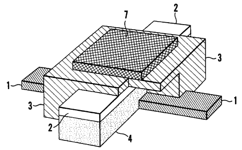
3o shown in perspective in fig. 3a, the first electrode 1 is
provided on a not shown substrate and for instance made
of aluminium. Above the aluminium electrode an
electrical isolating layer 4 is provided and on the top
CA 02297058 2004-O1-27
- 17
of the electrical isolating layer a second electrode 2 of
a second electrical conducting material, for instance
gold. Everywhere where the isolating layer 4 is not
covered by the gold electrode 2, it is etched away such
s that no direct contact is achieved in the intersection
between the electrodes 1, 2 and neither any electrical
contact. Over the intersection of the electrodes 1, 2
the contact layer 3 is provided and on the top thereof
and at the intersection such that it substantially
io extends somewhat beyond thereof, the functional element 7
is provided, for instance in the form of a sensitive
polymer.
If the functional element is to be used as a
basic element in a matrix device, such as is further
i5 discussed in connection with fig. 7, it must either be
connected to a diode structure and have an inherent
rectifying behaviour in order to avoid crosstalk problems
in passive addressing of the matrix device.
The principle structure of the functional
2o element 7 realized with a detecting function is shown in
fig. 3b. The first electrode 1, here indicated as a
metal electrode of aluminium, forms with a first polymer
material P1 in the form of PTOPT a rectifying Schottky
junction, wherein the metal forms the cathode. A second
z5 polymer material P2 forms the active or detecting element
itself and may be designed such that it changes its
conductivity by a physical or chemical stimulus. The
second electrode 2 which is designed as a metal electrode
of gold, comprises the anode of the structure and forms a
3o non-rectifying connection with polymer P1 (PTOPT).
Aluminium was selected as the metal of the first
electrode, as it has such a low work function as 4.3 eV.
CA 02297058 2004-O1-27
- 18
The gold anode has a higher work function, namely 5.2 eV.
With the use of a structure or geometry as shown
in fig. 3b it is possible to monitor the conductivity
state of the sensitive polymer P2 which here is denoted
as POWT, directly from the current-voltage
characteristics of the means. Experiments show that the
rectifying efficiency of a junction between A1 and doped
PTOPT was poorer than with a junction wherein undoped
PTOPT was used, even if the current strength for a given
to voltage was substantially higher. However, it is
regarded that the rectifying property of the junction is
more important than the bulk conductivity and hence
preferably undoped PTOPT was used in the sensor element.
As PTOPT is soluble in non-polar solvents, a
polymer soluble in polar solvents must be used for
sensitive polymer material, as the PTOPT layer otherwise
would be destroyed during a spin coating of this polymer.
A water soluble polythiophene was chosen, namely
poly(3[(S)-5-amino-5-carboxyle-3-oxapentyl)-2,5-
2o thiophenyl hydrochloride] (POWT). This molecule has an
unprotected amino acid side chain which shows a
remarkable solvent dependent specific rotation and
circular dichroism spectrum, something which is
interpreted as being caused by a partial interconversion
between syn- and antiorientations of the adjacent side
chains along the polymer chains. This polymer is also
soluble in methanol and dimethyl sulfoxide. It can be
doped with iodine (I2) or with a acetonitrile solution of
nitrocyltetrafluoroborate (NOBF4). This polymer material
(POWT) has the remarkable property that it is possible to
link different protein species to the amino acid side
chains of the molecule. Hence it may be possible to use
a protein which has the effect of changing the
CA 02297058 2004-O1-27
- 19 -
conductivity of the polymer as a reaction to the
biochemical stimulus, something which may be of great
interest if the functional element shall be used as a
detector for specific chemical reagents. The functional
s element 7 designed as a sensitive polymer may be spin
coated or deposited such that it forms a pattern on the
top of the contact layer 3, as this is shown in fig. 3a.
In this geometry the current will pass through the
sensitive polymer material and follow the current path
io which is mentioned, viz. from the second electrode 2 of
gold to a PTOPT layer and further through the sensitive
polymer POWT to the junction between the PTOPT and the
first electrode 1 of aluminium.
The functional element 7 may itself be a portion
i5 of the contact layer 3 which corresponds to the area
which is covered by the functional element as shown in
fig. 3a and the active areas of the functional elements
will then in reality correspond to the active area 3' as
shown in fig. 2b, viz. the portion of the contact layer 3
2o which is located on one side of the second electrode 2
and extends to the first electrode 1 where the side edge
of the first electrode intersects the other electrode.
Fig. 3c and fig. 3d show respectively a section and a
plan view of the electrode means wherein the functional
z5 element 7 is provided as a separate component on the top
of the contact layer 3 and over the intersection of the
electrodes 1,2. The functional element 7 may in any case
be accessed both from the first and the second electrode.
Depending on the material used in the functional element
30 7 it may have a detecting function, i.e. function as a
sensor, have an information storing function, i.e.
designed as an electrically addressable memory element or
it may have an information indicating function, e.g. by
CA 02297058 2004-O1-27
- 20 -
being designed as a radiation emitting element.
If the functional element 7 is realized with a
sensor function, it may be for instance be made such that
it gives a variable resistance as a result of a stimulus,
s for instance as a response to a biological material, a
chemical reagent, light radiation or pressure, and the
output signal will be a current. The functional elements
7 may also be designed in a material whose electrical
properties may be controlled or changed by applying a
lo voltage or injection of current and charge.
If the functional element 7 particularly is
realized with conjugated polymers as mentioned above, the
electrical or photoelectrical properties of these
materials make it possible to detect the presence of
i5 dopant species or incident light by the conductivity of
the material being changed. In addition also conjugated
polymers, as mentioned, may emit light by forming domains
which function as light-emitting domains. Further it
is possible to modify properties of conjugated polymers
2o in this respect by tuning their sensitivity and
selectivity vis-a-vis a specific chemical reagent or to a
specific wavelength. A number of conjugated polymers has
these properties, but particularly it has been preferred
using substituted polythiophenes (PTOPT).
2s With reference to figs. 4, 5 and 6 it shall now
be described how the functional element may be addressed
and controlled.
Fig. 4 shows a section through an electrode
means with a functional element 7 in the form of a sensor
3o element provided over the contact layer 3 at the
intersection of the electrodes 1, 2. The material in the
functional element 7 must in this case be a conductor,
CA 02297058 2004-O1-27
- 21 -
e.g. of organic or inorganic metal or semiconductor.
Specifically the electrode means in fig. 4 is shown
adapted for voltage addressing with regard to for
instance writing of a liquid crystal element provided
over a functional element 7. The liquid crystal element
may then be regarded as a pixel in a liquid crystal
screen. The liquid crystal element 8 contacts an
electronic conductor 9 which forms a third electrode of
the electrode means. The intention is now that the
to voltage addressing takes place with a waveform such that
some specific process which in this case will be the
orientation state of the liquid crystal element 8, is
controlled.
If the electrode means in fig. 3a is used for
i5 driving a liquid crystal display, it is only necessary
with voltage as the driving does not require particularly
high currents. If the liquid crystal element in fig. 4
are interchanged with an electroluminescent element 10,
this will require substantially higher currents, but the
2o principle for driving is once more very similar to that
for driving of the liquid crystal display. In this case
the electronic isolator 8, i.e. the liquid crystal
element, is replaced by a homogenous layer 10 of an
electroluminescent material, preferably conjugated
25 polymer, as this is shown in fig. 5. Over the
electroluminescent layer 10 there is once again provided
a third electrode 9 in form of an electronic conductor 9
which covers the whole layer and it is addressed
simultaneously with the functional element 7 such that
3o current passes through the electroluminescent layer 10.
In this connection it is essential that a sufficiently
high current can be injected in the functional element 7
such that the polymer material in the electroluminescent
CA 02297058 2004-O1-27
- 22 -
layer 10 becomes light-emitting. The functional element
7 is here a current injectable inorganic or organic metal
or a current injectable semiconductor.
If the functional element 7 is realized as a
s charge-storing inorganic or organic metal or a charge
storing semiconductor, it may further comprise
electroactive or electrochromic materials. The
electrochromic material may once again preferably be a
conjugated polymer and the functional element may now be
io realized as a pixel in an electrochromic image screen as
it is shown in fig. 6. Above the functional element 7
there are in this case provided a solid electrolyte layer
11, preferably in the form of a thin film of polymer
electrolyte, and thereabove a third electrode 12 of an
i5 electroactive material. By current and charge addressing
of the functional element 7 the state of the
electrochromic material with a functional element 7 will
change when a current passes through the polymer
electrolyte 11 and the overlying electroactive electrode
20 12. When this takes place, the colour of the
electrochromic material in the functional element 7
changes and this change will continue until the injected
charge once again disappears. This is the basis of
electrical addressing of electrochromic thin-film screens
2s which may be used for reversible registration of
information. Addressing and writing to the electro-
chromic film screen must then be combined with a reading
of the state of the functional element 7. As most
electrochromic materials also change their resistivity
3o when the doping state changes, it is possible first to
control this by injecting current through the functional
element 7 which is contacting the electroactive
counterelectrode 12 over the interposed solid electrolyte
CA 02297058 2004-O1-27
- 23 -
11 or polymer electrolyte. This changed doping state may
thereafter be found by addressing the functional element
7 with a current and reading the resistance of the
functional element. Preferably there may in this regard
also be provided an electronic conductor 9 above the
electroactive electrode 12. This may be used for
realizing a memory element. Even if writing and reading
in this case takes place with low speed, this embodiment
makes it possible to integrate such memory elements in a
io two-dimensional matrix and stack such matrices above each
other, such that a volumetric data storage device is
obtained.
The electrode means as shown in fig. 3a and in
figs. 4, 5 and 6 may easily be integrated in a quasi two-
dimensional matrix to an electrode device 13 wherein the
electrodes 1, 2 in the separate electrode means now forms
continuos strip-like structures which respectively
comprise rows and columns of electrodes 1, 2 in the
matrix, the rows in the following being denoted as the x
2o electrodes and the columns as the y electrodes of the
electrode device.
The electrode device 13 implemented as a two-
dimensional matrix is shown in approximate block diagram
form in fig. 7. The matrix which more correctly may be
denoted as a quasi two-dimensional matrix, as it
necessarily must have a certain thickness, is over a line
14 for the drive voltage or the row electrodes of the x
electrodes connected with an I/O converter board 16 while
a line 15 for the output signals from the y electrodes
3o similarly is conveyed to the I/O converter board 16. The
output signals from the y electrodes are converted into a
voltage and output on a line 17 to an A/D converter board
20 wherefrom the digitalized output signals or response
CA 02297058 2004-O1-27
- 24 -
signals may be conveyed further to a suitable data
processing device on a data bus 21. The data processing
device may be a common PC or a dedicated work station,
and it is not shown in the figure. A line 19 for the
s drive voltage of the row electrode, i.e. their bias
voltage, is similarly conveyed from the A/D converter
board 20 and to the I/0 converter board 16 together with
the selector line 18 for selecting the electrode row to
be driven. In the matrix of the electrode device 13 the
io contact layer 3 may now integrated form a global contact
layer in the matrix such that the electrical conducting
or semiconducting material of the contact layer are
located over both electrode layers and contacts these
electrically. The functional elements 7 for each
15 electrode means may be provided in the contact layer and
form a part thereof, the functional element then being
formed at the intersection of an x electrode and a y
electrode in each electrode means which are included in
the matrix of the electrode device 13. The functional
2o element 7 may also be provided as separate element and
assigned to each of the electrode means, such this is
shown in fig. 2a. In principle that may take place by
the functional element 7 being provided in a layer above
the contact layer 3 and patterned such that separate
2s functional elements are obtained for each electrode means
2. This is, however, no prerequisite as the functional
elements 7 very well may be formed in an unpatterned
layer of material which forms the functional elements and
which is deposited over the contact layer 3. First by
3o the addressing the functional element 7 is generated as
an active structure assigned to the separate electrode
means in the matrix.
The electrode device in fig. 7 may also be
CA 02297058 2004-O1-27
- 25 -
provided with more than one layer of functional elements
7, as the separate layer of functional element then must
be separated by an electronic or ionic conductor layer.
Fig. 8 shows a simplified electrical equivalent
model of the network formed by the x electrodes and y
electrodes 1, 2 in the matrix of the electrode device 13
in fig. 7. At each intersection between the row
electrodes and the column electrodes a diode 23 which in
each case has the same conduction direction, is
io generated. Possibly the electrode device may also be
realised with an inherent rectifying function in order to
avoid crosstalk problems by addressing, cf. the
description above of the functional element in connection
with fig. 3a and the immediate preceding section. The
i5 selective addressing of the separate electrode means 26
namely requires that a rectifying contact is present in
each electrode means, for instance between the first
electrode 1 and the contact layer 3. When the functional
element 7 in an electrode means 26 in an x,y position in
2o the matrix shall be read, a current transition between
adjacent locations (x+l,y), (x-l,y),(x,y+1) or (x,y-1)
must not take place. This is evident from fig. 8
wherefrom it is seen that two opposite diodes block a
current transition of this kind.
2s With the electrodes provided in matrix form in
the electrode device, such as shown in fig. 8, current
only will pass through the contact layer 3 or between the
electrodes 1, 2 in the active area 3' such as shown in
fig. 2a. If simultaneously for instance a physical or
3o chemical stimulus changes the conductive properties of
the polymer material in this area, for instance due to
incident light, the change will be detected by
application of voltage and reading of the corresponding
CA 02297058 2004-O1-27
- 26 -
current of the output signal. If the electrodes 1, 2 in
an electrode device are floating, i.e. the x electrode 1
is not biased, the current from the functional elements
will also pass through adjacent functional elements in
s the electrode means with floating electrodes. This
problem is solved by earthing the electrodes 2 as this is
shown in fig. 8 by using current/voltage converters 22 in
all columns between their output and earth. As the input
impedance of these current/voltage converters 22 is
io negligible, all column electrodes may be regarded as
grounded. Preferably a buffer voltage was supplied to a
selected row electrode 1;25 as all other electrodes 1;24
were floating. Then two advantages are obtained, namely
that the current in each column of the other electrodes 2
1s only depends on the functional element identified by this
column and the selected row and that all functional
elements in the same row in principle may be monitored
simultaneously. By monitoring of the electrode device
there was in one embodiment used a specially designed
2o converter board 16 for current-to-voltage conversion
which also applied the positive bias current to the
chosen row 1', while a commercially available A/D
converter board was used. The electrode device 13 may
preferably be software-controlled over for instance a PC
2s as this is indicated in fig. 7, and it will over an
interface of this kind be possible to select the voltage
which can be applied to the rows and a possible waiting
time before the first measurement is taken. The last
feature is expedient with regard to avoiding transient
ao phenomena such as capacity currents and it has in
practise turned out advantageous to wait about 200 ms.
The detected output currents may have a magnitude of a
few pA such that noise generated from a network in the
matrix thus may be a source of error. This disadvantage
CA 02297058 2004-O1-27
- 27 -
may be alleviated to some degree by including a very
simple lowpass filter implementation by reading each
functional element a number of times at a frequency
selected by the user and average the measured values, As
s expected the best results were achieved by using
monitoring periods which was a multiple of the voltage
period of the network.
If the functional element in the layer is
realized not as a global, but as a patterned layer, it
io will contact both the x and the y layers through the
anisotropic conductor of the contact layer 3. By
patterning the functional element 7 in the layer, neither
separate functional element will shortcircuit to the
adjacent functional element. It is, of course, thinkable
i5 with applications wherein the functional element layer is
unpatterned and global. The functional element layer may
then be a material which is in ohmic contact with the
anisotropic conductor, but it may also be made such that
it forms a rectifying contact with the anisotropic
2o conductor in the contact layer 3. If the functional
element 7 is formed with an ohmic contact, the resistance
in the separate functional element may be measured by
addressing the separate functional element, i.e.
addressing the x,y position in the matrix. In this case
2s the material of the functional element may for instance
have a specific chemical response output and deliver an
output signal in the form of a changed resistance when it
is in contact with a chemical species. It may also be a
biosensitive material which provides a resistance change
3o by interaction with biomolecules and biosystems, a
piezoresistive material wherein applied pressure changes
the resistance of the functional element, a
photoconductive material wherein light changes the
CA 02297058 2004-O1-27
- 28
resistance of the functional element, or a thermally
sensitive material wherein heating changes the resistance
of the functional element. The last cases cover a number
of advantageous applications of the invention which each
s may be denoted as respectively a chemical camera, a
biocamera, a photocamera and a thermocamera. Generally
any interaction which changes the conductivity or
resistance of the functional element may be read by using
such an embodiment of the electrode device 13,
io irrespective whether the interaction has a physical,
chemical or biological cause. Dependent on the function
or the application the respective size of each separate
functional element which in a camera application may be
regarded as individual pixels in the camera, may be from
i5 1 ~.m to 1 cm depending on the scale of object to be
imaged. If the camera for instance shall image the local
pH value at a biological cell, the functional element
will be selected with dimensions with a magnitude of a
few micrometers.
2o If the electrode device shall be manufactured as
a number of identical and reproduceable devices, these
may be made in a scale between 10 ~,m and 1 cm, such that
the layers in the electrode device become homogenous over
these dimensions. It is also thinkable that realization
2s of the electrode device according to the invention in a
camera application, particularly for detection of
chemical reagents or biomolecules in a chemical camera
respectively a biosensor with simultaneous detection of
many substances and interactions, may be designed with
3o functional elements to be used only once and possible
combined with methods for positioning the functional
elements at different locations on a surface. Another
thinkable application is the use of chemically sensitive
CA 02297058 2004-O1-27
- 29 -
but non-specific polymers and combining a number of
different materials in the functional element, for
instance deposited by inkjet printing to different
functional elements in the device such that it becomes
s possible to realize what may be described as an
artificial chemical or biological sense organ for the
detection of odour- or flavour-emitting substances in a
gas or liquid environment where it is desirable to detect
the presence of chemical or biological interactions.
io The electrode device 13 according to the
invention may also comprise a contact layer 3 which has
no anisotropic conductor, but wherein the 'contact layer
which consists of a homogenous material which may react
to biomolecules, chemical reagents, light or pressure, is
i5 deposited directly over the electrode structure. The
functional element 7 will then be included in and form a
part of this contact layer 3 and function as detectors
where the active areas once again corresponds to edge
areas 3' as shown in fig. 2 and make possible detection
20 of changes or specific characteristics in these active
areas 3' when it is subjected to specific stimuli. The
specific changes may for instance be a change of
resistivity, capacitance or the current/voltage
characteristics.
25 The_electrode device 13 according to the
invention may find application as a data processing
device if the functional elements 7 are adapted such that
they may be switched between different states and
possibly be used for configuring logic gates or logic
3o networks. Another and obvious application is using the
electrode device 13 according to the invention as an
electrically addressable data memory. Writing then takes
place in each memory cell in the memory device, as the
CA 02297058 2004-O1-27
- 30 -
memory cell corresponds to the separate electrode means
26 and the memory device to the electrode device 13. The
contact layer 13 itself may in this case advantageously
function as a memory material and writing to a memory
s location, i.e. to the separate memory cell, may take
place by changing the electrical properties of the
contact layer in the active area in each electrode means
26 or memory cell. For instance may writing take place by
destroying the conductivity such that there no longer is
io electric contact between the electrodes 1, 2 at the
memory location in question. Possibly the memory device
13 may be realized such that the conductivity gradually
is reduced. If this reduction takes place in
predetermined steps, each memory location can store
i5 several bits and it will be possible storing bits
according to a predetermined multilevel code. The storage
density can thus be increased in a substantial degree. A
closer description of the method for electrical
addressing of a memory device and a discussion of
2o complete embodiments of such memory devices are found in
NO patent application No. 972803 filed on 17 June 1997
and assigned to the present applicant. - Memory devices
of this kind may also be designed volumetrically by
stacking electrode devices above each other.
2s Particularly with the use of coding in each memory
location it will then be possible to obtain electrically
addressable memory devices with an extremely high
volumetric storage density.
The electrode device 13 according to the
3o invention may also be used as an optical camera or
electronic camera by realizing the contact layer or the
functional layer as a photodiode matrix. This may for
instance take place by using a well-known photodiode
CA 02297058 2004-O1-27
- 31 -
material, e.g. conjugated polythiophene mixed with
buckministerfullerene Cso in the contact layer. The
function of a camera of this kind is indicated wholly
schematically in fig. 9.
s The electrode device 13 can as mentioned above
also be employed as a chemical camera, strictly spoken a
chemical sensor for instance to detect a specific
distribution of a chemical substance as indicated
schematically in fig. 10. It may then be used a
1o functional element comprising a polymer layer of PTOPT.
It is the absence of barriers against mass
transport to the polymer layer in the electrode device
which makes it suitable for chemical detection, i.e. as a
chemical camera. Since conjugated polythiophenes may
1s interact with oxidating chemical species such that a
highly conducting polymer material is formed, this may
for instance be regarded as a model system for a chemical
camera of this kind. It is for instance well-known that
vapour of iodine will oxidize polythiophenes, including
2o PTOPT which preferably is used in the present invention.
This results in an increase in the conductivity of many
magnitudes. Hence the functional element 7 may be
addressed electronically such that the doping process
which may be visualized in the form of an increased
2s conductance, may be followed.
Fig. 10 shows schematically the result achieved
by detection of iodine crystals on the detector of a
chemical camera designed according to the invention and
with the electrodes respectively of aluminium and gold
3o with the use of an isolating layer of benzocyclobutene
covered with PTOPT which forms both the contact layer and
the functional element layer.
CA 02297058 2004-O1-27
- 32 -
The electrode device 13 according to the
invention may also be employed in a display device,
indicated schematically in fig. 11 by for instance being
driven such that the functional element becomes
electroluminescent. In the same structure as used for the
application described in connection with fig. 9 it may
also be possible to generate light emission. In an
embodiment conjugated polythiophene was used in the
functional element layer and deposited over electrodes of
to indium tin oxide which was supplied with a voltage of
+ 30 V with simultaneous grounding of the aluminium
electrodes (row electrodes). The light source pixels are
easily visible to the naked eye. In an embodiment the
polymer pixels emit red light. By applying voltage to a
i5 specific electrode means in the electrode device light
will be emitted from this electrode means only.
With the electrode means 26 and the electrode
device 13 according to the present invention the great
advantage is achieved that the functional element or the
2o material in the functional element layer is exposed to
and accessible from the environment simultaneously as it
can be addressed electrically and hence make possible the
detection of substances and stimuli to which the
functional element material is sensitive.
25 The manufacture of the separate parts of the
electrode means according to the invention is as per se
known and for instance described in other connections,
e.g. in the above-mentioned international patent
application PCT/SE95/00549 and in a paper by M. Berggren,
3o O. Inganas & al. "Light emitting diodes with variable
colours from polymer blends" Nature 1994, Vol. 372, p.
44. Yet as a guide for persons skilled in the art there
is in a separate appendix furnished examples which are
CA 02297058 2004-O1-27
- 33 -
regarded as specific and informative in relation to the
means according to the present invention. These examples
are directed towards the manufacture of an anisotropic
conducting material, the manufacture of the electrode
s means on a substrate and the application of the
functional element layer to the electrode means according
to the invention and both with and without the use of an
anisotropic conductor.
to APPENDIX
Example 1: Forming of an anisotropic conducting material
mg/ml poly[3-(4-octyl-phenyl)-2.2~-bithiophene] (PTOPT)
is dissolved in chloroform and 5/mg/ml of
polymethylmetacrylate (PMMA) likewise dissolved in
i5 chloroform. A mixture was formed from these solutions to
prepare a solution of 6% PTOPT in PMMA. This solution is
then spin coated onto a substrate at a rotation speed of
800 rpm to give a film with a thickness about 100 nm. The
film thickness will then be comparable to the domains of
2o the conjugated polymer, so that electrical conductivity
normal to the film is high, and parallel to the film is
negligible. If desired it is possible to convert the
PTOPT to the doped form by exposing it to gaseous
oxidants or to oxidants in solutions which will not
2s dissolve the two polymers. If the polymer blend is
deposited on a conducting substrate it is also possible
to dope it to the conducting state by electrochemical
doping.
CA 02297058 2004-O1-27
- 34 -
Example 2: Forming of an anisotropic conducting material
mg/ml poly(3-octyl)-thiophene (POT) is dissolved in
chloroform and 5 mg/ml of polymethylmetacrylate (PMMA)
likewise dissolved in chloroform. A mixture was formed
s from these solutions to prepare a solution of 5~ POT in
PMMA. This solution is then spin-coated onto a substrate
at a rotation speed of 800 rpm to give a film of about
100 nm thickness. The film thickness will then be
comparable to the domains of the conjugated polymer, so
io that electrical conductivity normal to the film is high
and parallel to the film is negligible. If desired it is
possible to convert the POT to the doped form by exposing
it to gaseous oxidants or to oxidants in solutions which
will not dissolve the two polymers. If the polymer blend
i5 is deposited on a conducting substrate it is also
possible to dope it to the conducting state by
electrochemical doping.
Example 3: Forming of an electrode device on a silicon
c"1-,~t,-~to
zo A silicon chip is covered by aluminium strips (the x
electrodes 250 nm thick) evaporated through a shadow
mask. A layer of benzocyclobutene (BCB; (CycloteneT"', Dow
Chemical) is spin coated at 1000 rpm for 30 seconds from
a solution of BCB 1:10 in mesitylene, to make a film of
2s 200-400 nm thickness. The film is cured at 250°C for 60
minutes. A layer of gold (50nm), undercoated with a 2 nm
thick layer of Cr for adhesion, is evaporated through a
shadow mask defining the y electrodes. The chip is etched
in a plasma by reactive ion etching for 2 minutes. This
30 leaves the gold electrodes unaffected, but removes the
BCB from all other surfaces. The aluminium electrodes are
exposed after this etching procedure. Anisotropic layers
are deposited according to Example 1.
CA 02297058 2004-O1-27
- 35 -
Example 4: Forming of an electrode device on a glass
"~...~v-,~.,
A glass substrate is covered by benzocyclobutene (BCB) by
spin coating and curing. This is used as the substrate
for depositing further layers. The surface is covered by
aluminium strips (the x electrodes, 50 nm thick)
evaporated through a shadow mask. A layer of BCB
(CycloteneT"", Dow Chemical) is spin-coated at 1000 rpm for
30 seconds from a solution of BCB 1:10 in mesitylene, to
to make a film of 200-400 nm thickness. The film is cured at
250°C for 60 minutes. A layer of gold (50nm), undercoated
with a 2 nm thick layer of Cr for adhesion, is evaporated
through a shadow mask defining the y electrodes. The chip
is etched by reactive ion etching for 2 minutes. This
i5 leaves the gold electrodes unaffected, but removed the
BCB from all other surfaces. The aluminium electrodes are
exposed after this etching procedure. Anisotropic layers
are deposited according to Example 1.
Example 5: Deposition of a functional element layer
2o A device according to Example 3 is covered with a
homogenous thin film of poly(3[(S)-5-amino-5-carboxyl-3-
oxapentyl)-2,5-thiophenylene hydrochloride] (POWT) by
solvent casting from a polymer solution. The resistance
of each pixel of POWT is recorded. A small crystal of
25 iodine is positioned at a pixel. The iodine is a dopant
for POWT and the presence of iodine can be read as a
decrease of resistance at the pixel.
Example 6: Electrode device without an anisotropic
,. .,., ,a , , ~ ,- ,. v.
3o A device according to Example 3, but without the anisotropic
conductors, is covered with a homogenous film of poly[3-(4-
octyl-phenyl)-2.2~bithiophene (PTOPT) in a 5 mg/ml xylene
solution and C6o (buckministerfullerene) in a 5 mg/ml xylene
CA 02297058 2004-O1-27
- 36 -
solution. The film is formed by spin-coating at 400 rpm from
a warm solution (50°C). This film is photoresponsive, and
local changes in the photocurrent or resistivity upon
exposure to light can be detected.