Note: Descriptions are shown in the official language in which they were submitted.
CA 02297353 2000-O1-27
POWER AMPLIFIER ARRANGEMENT
The invention relates to a power amplifier arrangement with high current
drive capability, particularly but not exclusively for transmission systems.
In several transmission systems, such as Asymmetric Digital Subscriber
Line, video distribution and audio, there is a need to transmit signals with
high
crest factors (peak/rms). This high crest factor results from short signal
peaks that
'~~ rarely occur, but which force the driver to be supplied from a high
voltage supply.
This results in a high dynamic power consumption in the amplifier.
In the seventies amplifiers were developed with lower power consumption,
more particularly the class G amplifiers working at two different supply
voltages.
They use one large output stage, biased by two different voltage supplies,
whereby diodes are generally used to control the switchover from the low
voltage
to the high voltage supply. Such G class transistor amplifiers are amongst
others
disclosed in US-A-3.772.606 and US-A-4.100.501.
In case the transistors of the classical G class amplifiers have to drive
large currents, they may be replaced by Darlington pairs, such as for instance
disclosed in the above-mentioned US-A-4.100.501. In this prior art document,
the described push-pull variant comprises two Darlington pairs having together
four transistors of the same conductivity type and two Darlington pairs having
together four transistors of the conductivity type opposite to that of the
first
mentioned Darlington pairs. The transistors of the first and second Darlington
pairs conduct during each positive half cycle of the input signal. The
transistors
2~ of the third and fourth Darlington pairs conduct during each negative half
cycle
of the signal. The collectors of the two transistors of a first Darlington
pair are
connected to each other and to a positive D.C. high voltage supply. Similarly,
the
collectors of the two transistors of a fourth Darlington pair are connected to
each
other and to a negative D.C. high voltage supply. In this prior art embodiment
the collectors of the two transistors of the second Darlington pair are also
CA 02297353 2000-O1-27
connected to each other and via a diode to a positive D.C. low voltage supply,
while the two transistors of the third Darlington pair are connected to each
other
and via another diode to a negative D.C. low voltage supply. The emitter of
the
output transistor of the first, respectively fourth, Darlington pair is
coupled to the
collectors of both transistors of the second, respectively third, Darlington
pair.
This prior art solution whereby each transistor of the original class-G
amplifier is replaced by a Darlington pair, results in a high current
amplification
and consequently a high current drive capability, but at the same time in a
large
voltage drop across all Darlington pairs.
The invention seeks to provide an amplifier with high current drive
capability , with relatively low dynamic power consumption, but avoiding such
a
large voltage drop across the transistors.
In accordance with the invention, this object is accomplished in an
amplifier of the G class type, comprising at least one set of two transistor
pairs
having together four transistors of the same conductivity type with an input
electrode, a common electrode and an output electrode, each pair comprising
an input transistor and an output transistor in cascade, the output electrode
of the
input transistor being coupled to the input electrode of the output
transistor,
whereby means are provided for applying an input signal to the input
electrodes
of the input transistors of both pairs and both pairs are biased by two
different
voltage s~~pplies, control means being provided for switching over from the
voltage of one voltage supply to the voltage of the other voltage supply, the
transistors of the first pair of a set being coupled in a Darlington circuit
arrangement, characterized in that both transistors of the second pair of said
set
have their common electrodes separated from each other, the common electrode
of the input transistor of said second pair being coupled to the output
electrode
of the input transistor of the first pair and the common electrode of the
output
transistor of said second pair being coupled to the output electrode of the
output
transistor of the first pair.
By disconnecting from each other the common terminals of the transistors
CA 02297353 2000-O1-27
3
of the second pair and by putting in series the input transistors of both
pairs, the
voltage drop is reduced and the dynamic range of the amplifier at the lower
supply voltage is increased. This can in turn result in a lower value of this
lower
supply voltage, which again results in a lower power consumption, being the
main benefit of the invention.
Remark that in the claims and throughout this document, the expression
"common electrode " is to be interpreted with reference to the configuration
of
the circuit of which the transistor having this common electrode forms part.
In this
respect, as is described in all standard electronics handbooks, the common
electrode is common to both the input and the output circuit, as opposed to
either
the input or the output electrodes themselves. This common electrode,
corresponds to the " common" or ground from ac point of view.
The input electrode of the transistors may be the base, the common
electrode the collector and the output electrode the emitter, as described by
claim
2.
In such case, the collectors of both transistors of the first pair of a set
are
coupled to a first D.C. voltage supply, the emitter of the output transistor
of the
first pair and the collector of the output transistor of the second pair of
the set are
coupled to each other and to a second D.C. voltage supply with a voltage which
is in absolute valuelower than the voltage provided by the first voltage
supply, the
means for applying an input signal being coupled to the bases of the input
transistors of both pairs, and the collector of the input transistor of the
second
pair being coupled to the emitter of the input transistor of the first pair
and thus
disconnected from the collector of the output transistor of the second pair
and
thus also disconnected from the emitter of the output transistor of the first
pair.
In addition, a drive control circuit coupled between the means for applying
an input signal, and the input terminals of the transistor pairs, may comprise
diodes coupled between the input transistors of the two pairs and the means
for
applying this input signal, as is described in claims 3 and 4.
The control means for switching over from one voltage to the other can
CA 02297353 2000-O1-27
4
include a diode in a connection between the second lower D.C. voltage supply,
on the one hand, and the output electrode of the output transistor of the
first pair
and the common electrode of the output transistor of the second pair, on the
other hand.
The control means for switching over from one voltage to the other may
also include a diode in a connection between the second lower D.C. voltage
supply, on the one hand, and the output electrode of the input transistor of
the
first pair and the input electrode of the output transistor of the first pair,
on the
other hand.
The means for applying an input signal may include an A.C. input signal
source, this signal being a current or a voltage, in which case the amplifier
contains two sets of two transistor pairs, one set for the positive half cycle
of the
input signal and one set for the negative half cycle of the input signal,
whereby
the transistors of the second set are of the opposite conductivity type to
that of the
transistors of the first set and the two voltage supplies for the second set
are of
a polarity opposite to the polarity of the voltage supplies for the first set.
In this case, the amplifier may more po~+~~rrlarly comprise a second set
with third and fourth pairs similar to the second and first pairs of the first
set,
whereby thus the emitter of the input transistor of the fourth pair, which is
a
Darlington pair, is coupled to the base of the output transistor of this
fourth pair
and coupled to the collector of the input transistor of the third pair. The
collectors
of both transistors of the third pair are thereby again disconnected from each
other. The collectors of both transistors of the fourth pair are coupled to a
third
D.C. voltage supply whereby the emitter of the output transistor of the fourth
pair
and the collector of the output transistor of the third pair are coupled to
each
other and to a fourth D.C. voltage supply providing a voltage which is lower
in
absolute value than the voltage provided by third D.C. voltage supply, and
whereby further the bases of the input transistors of the third and fourth
pairs are
coupled to the means for applying an input signal and the emitter of the
output
transistor of the third pair is coupled to the emitter of the output tr-
ansi:;;~ ~~ ~~ ~!-;_:
CA 02297353 2000-O1-27
second pair.
The invention will now be described by way of example and with reference
to the accompanying drawing which is a schematic circuit diagram of an
amplifier according to the invention.
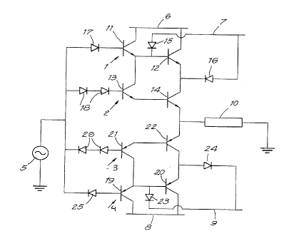
S The amplifier circuit represented in the drawing is a G class amplifier
comprising essentially a first set of two transistor pairs 1 and 2, a second
set of
two transistor pairs 3 and 4, an A.C. input signal source 5, a first, positive
high
D.C. voltage supply 6, a second, positive low D.C. voltage supply 7, a third,
negative high D.C. voltage supply 8 and a fourth, negative low D.C. voltage
supply 9. The output terminal of the second transistor pair, coupled to the
output
terminal of the third transistor pair constitutes an output terminal of this
amplifier
circuit, which is in general coupled to a load 10.
The first transistor pair 1 consists of an input transistor 1 1 and an output
transistor 12 coupled in Darlington circuit arrangement, and is thus what is
called
a Darlington pair, whereby consequently the emitter of transistor 1 1 is
coupled
to the base of transistor 12 and the collectors of both transistors 1 1 and 12
are
coupled to each other and to the first D.C.voltage supply 6.
The second transistor pair 2 consists of an input transistor 13 and an
output transistor 14, whereby the emitter of transistor 13 is coupled to the
base
of transistor 14. However, the collectors of both transistors 13 and 14 are
not
coupled to each other and this second pair 2 is therefore not a Darlington
pair.
All transistors 1 1 to 14 are of the same conductivity type, in the
illustrated
example of NPN type.
The second, low voltage supply 7 is coupled through a diode 15 to the
junction between the emitter of transistor 1 1 and the base of transistor 12.
The
diode 15 avoids that the transistor 12 receives a reverse voltage, while at
the
same time also assuring the switchover from the current from the second D.C.
voltage supply 7 to the first voltage supply 6 when the input signal exceeds a
certain level which is related to the voltage provided by the second voltage
supply
3O 7.
CA 02297353 2000-O1-27
G
The collector of the output transistor 14 of the second pair 2 is coupled to
the emitter of the output transistor 12 of the first pair 1 by means of a
junction to
which the second lower voltage supply 7 is also coupled through another diode
16. This emitter of the output transistor 12 is not coupled to the collector
of the
input transistor 13 of the second pair 2.
The emitter of the input transistor 11 of the first pair 1 is coupled to the
collector of the input transistor 13 of the second pair 2.
To the emitter of transistor 14 of the second pair 2 one terminal of the
t
load 10 may be coupled, the other terminal of the load being grounded.
The base of the input transistor 1 1 is coupled to one terminal of the A.C.
input signal source 5 through a diode 17, while the base of the input
transistor
13 is also coupled to this terminal but through two series-coupled diodes 18.
The
other terminal of the source 5 is grounded.
The diodes 17 and 18, forming part of the drive control circuit, assure a
difference in drive voltage to the transistors 11 and 12, but it is obvious
that this
voltage difference may be obtained by other means than said diodes 17 and 18.
Thus other embodiments of such a drive control circuit exist, and are commonly
known by a person skilled in the art.
The third and fourth transistor pairs 3 and 4 are respectively similar to the
above mentioned second and first transistor pairs 2 and l, with this
difference
that their transistors 19, 20, 21 and 22 are all of a same conductivity type
which
is however of the opposite type to that of transistors 1 1, 12, 13 and 14 and
are
consequently of the PNP type in the illustrated example.
The fourth transistor pair 4 is similar to the first pair 1 and forms the
first
pair of the second set of pairs. This fourth pair 4 consists of an input
transistor 19
and an output transistor 20 coupled in a Darlington circuit arrangement. The
emitter of transistor 19 is coupled to the base of transistor 20 whereas the
junction point is coupled through a diode 23 to the fourth, negative low D.C.
voltage supply 9, while the collectors of both transistors 19 and 20 are
coupled
to the third negative high D.C. voltage supply 8.
CA 02297353 2000-O1-27
7
In a lot of embodiments, except for the sign, the higher voltages of the
supplies 6 and 8 are equal in value, while the lower voltages of the supplies
7
and 9 are also equal in value but of opposite sign. However in other
embodiments asymmetrical voltage values can be the case. In the most general
case the first supply voltage is more positive than the third supply voltage,
the
second supply voltage is more positive than the fourth one, the difference
between the first and the third is larger than the difference between the
second
and the fourth supply voltage, and the voltages between the second and fourth
supply voltage , are lying within the range of voltages between the first and
the
third supply voltage.
The third pair 3 is similar to the second pair 2. It forms the second pair of
the second set of pairs and consists of an input transistor 21 and an output
transistor 22. The emitter of transistor 21 is coupled to the base of
transistor 22.
The collector of the input transistor 21 is coupled to the emitter of the
input
transistor 19 of the fourth pair 4 but is not coupled from the emitter of the
output
transistor 20 of this fourth pair 4, while the collector of the output
transistor 22
is coupled to the emitter of the output transistor 20, the junction being
coupled
through a diode 24 to said fourth negative low D.C. voltage supply 9.
The emitter of the output transistor 22 of the third pair 3 is coupled to the
output terminal, which is further coupled to the load 10.
The bases of the input transistors 19 and 21 are coupled through a diode
25, respectively through a series-connection of diodes 26 with the A.C. input
signal source 5.
The set of transistor pairs 3 and 4 operates as a complementary circuit to
the set of transistor pairs 1 and 2. The transistors 11 and 13 conduct during
each
positive half cycle of the input signal. The transistors 19 and 21 conduct
during
each negative half cycle of the signal, a push-pull mode of operation being
carried out.
Output signals from the input transistors 1 1, 13, 19 and 21 are fed to the
output transistors 12, 14, 19 and 22, respectively, where they are further
CA 02297353 2000-O1-27
8
amplified and fed to the load 10.
The amplifier further operates as a G class amplifier, the pairs 1,2 and
3,4 of both sets being biased by two different voltages.
Important is that, due to the fact that the collectors of the transistor 13
and
14 of the second pair 2 are not in contact with each other, the emitter of the
output transistor 12 of the first pair 1 is not coupled to the collector of
the input
transistor 13 of the second pair 2, this collector being coupled to the
emitter of
the input transistor 1 1 of the first pair 1. Consequently, the transistor 13
receives
,;
r
a higher voltage. Thus transistor 13 will be able to drive transistor 14 with
a
higher voltage, thereby reducing the voltage drop over transistor 14 since the
emitter of transistor 14 will be as well driven at a higher voltage while the
collector voltage is kept at the second low voltage supply via the diode 16 in
case
the output current is supplied by the second D.C. supply voltage.
The same applies to the transistors 21 and 22 of the third pair 3. The
collectors of these transistors 21 and 22 are not coupled to each other and
the
emitter of the output transistor 20 of the fourth pair 4 is coupled to the
collector
of the output transistor 22 of the third pair 3 but not to the collector of
the input
transistor 21 of this third pair 3. The emitter of the input transistor 19 of
the
fourth pair 4 is coupled to the collector of the input transistor 21.
The dynamic range of the amplifier at the supply voltage of the low
voltage supply 7 or 9 is increased and this low supply voltage may be lower.