Note: Descriptions are shown in the official language in which they were submitted.
CA 02297738 2000-O1-24
WO 99/05731 PCT/US98115224
SOLID-STATE ENERGY STORAGE MODULE
EMPLOYING INTEGRATED INTERCONNECT HOARD
FIELD OF THE INVENTION
This invention relates generally to energy
storage devices, and more particularly, to an apparatus
and method for selectively interconnecting a number of
independent energy storage cells disposed in a sealed
housing.
BACKGROUND OF THE INVENTION
The demand for new and improved electronic and
electro-mechanical systems has placed increased pressure
on the manufacturers of energy storage devices to
develop battery technologies that provide for high
energy generation in a low-volume package. Conventional
battery systems, such as those that utilize lead acid
for example, are often unsuitable for use in high-power,
low-weight applications. Other known battery
technologies may be considered too unstable or hazardous
for use in consumer product applications.
A number of advanced battery technologies have
recently been developed, such as metal hydride (e. g.,
Ni-Nffi), lithium-ion, and lithium polymer cell
technologies, which would appear to provide the
requisite level of energy production and safety margins
for many commercial and consumer applications. Such
advanced battery technologies, however, often exhibit
characteristics that provide challenges for the
manufacturers of advanced energy storage devices.
CA 02297738 2000-O1-24
WO 99/05731 PCT/US98/15224
2
In accordance with a conventional advanced
battery design, individual cells are hardwired together
and to the positive and negative power terminals of the
battery. Various electronic components which may be
incorporated into the battery design must also be
hardwired to the cells. It can be appreciated that such
conventional interconnection approaches provide for
little, if any, flexibility when attempting to alter the
series and/or parallel hardwired connections between the
cells and components.
Moreover, the wiring process typically
employed in the fabrication of conventional advanced
batteries is generally complicated and time consuming.
An assembly defect of particular concern to the
manufacturers of conventional advanced batteries
involves unintentional wiring shorts which develop
during the wiring process. Such manufacturing defects
typically result in a reduction in the performance and
service life of the battery, and often represent a
significant safety concern.
Other characteristics of advanced battery
technologies provide additional challenges for the
designers of advanced energy storage devices. For
example, certain advanced cell structures are subject to
cyclical changes in volume as a consequence of
variations in the state of charge of the cell. The
total volume of such a cell may vary as much as five to
six percent during charge and discharge cycling. Such
repetitive changes in the physical size of a cell
significantly complicates the mechanical housing design
and electrical connection strategy. The
electrochemical, thermal, and mechanical characteristics
CA 02297738 2000-O1-24
WO 99/05731 PCT/US98/15224
3
of an advanced battery cell must typically be well
understood and appropriately considered when designing
an energy storage system suitable for use in commercial
and consumer devices and systems.
There is a need in the advanced battery
manufacturing industry for an energy storage device that
exhibits high-energy output, and one that provides for
safe and reliable use in a wide range of applications.
There exists a further need for an effective
interconnection strategy which provides flexibility and
reliability when interconnecting a number of independent
energy storage cells contained within a sealed housing
to meet specified current and voltage ratings. The
present invention fulfills these and other needs.
SU1~IARY OF THE INVENTION
The present invention is directed to an
improved electrochemical energy storage device. The
electrochemical energy storage device includes a number
of solid-state, thin-film electrochemical cells which
are selectively interconnected in series or parallel
through use of an integrated interconnect board. The
interconnect board is typically disposed within a sealed
housing or shell which also houses the electrochemical
cells, and includes a first contact and a second contact
respectively coupled to first and second power terminals
of the energy storage device. The interconnect board
advantageously provides for selective series or parallel
connectivity with the electrochemical cells,
irrespective of cell position relative to one another
within the housing. In one embodiment, a sheet of
CA 02297738 2000-O1-24
WO 99/05731 PCTIUS98/15224
4
conductive material is processed by employing a known
milling, stamping, or chemical etching technique to
include a connection pattern which provides for flexible
and selective interconnecting of individual
electrochemical cells within the housing, which may be a
hermetically sealed housing. The voltage and current
characteristics of the energy storage device are
alterable by altering the configuration of the
connection pattern. Fuses and various electrical and
electro-mechanical devices, such as bypass,
equalization, and communication devices for example, may
also be mounted to the interconnect board and
selectively connected to the electrochemical cells.
BRIEF DESCRIPTION OF THE DRAWINGS
Fig. 1 illustrates an embodiment of a solid-
state energy storage device which includes a stack of
thin-film electrochemical cells selectively
interconnected in a series and/or parallel relationship
by use of an interconnect board;
Fig. 2 illustrates a surface of an
interconnect board having a connection pattern disposed
thereon for providing selective series and/or parallel
connectivity with a number of electrochemical cells;
Fig. 3 is another illustration of an
interconnect board which includes a sheet of conductive
material including a connection pattern for selectively
connecting a number or electrochemical cells in a series
or parallel relationship;
CA 02297738 2000-O1-24
WO 99/05731 PCTIUS98/15224
Fig. 4A illustrates another embodiment of an
interconnect board which includes a number of components
mounted thereon;
Fig. 4B illustrates yet another embodiment of
5 an integrated interconnect board;
Figs. 5A-5C is an illustration of a component
package within which equalizer and bypass devices are
integrally incorporated;
Fig. 6 is an exploded view of an energy
storage module including an interconnect board disposed
in a hermetically sealed housing;
Figs. 7-9 illustrate an embodiment of a
hermetic seal for use in a sealing various types of
conduits or feed-throughs that pass into a module
housing;
Fig. 10 is an illustration of a prismatic
electrochemical cell which represents one
embodiment of an energy storing device which may be
used in combination with an integrated interconnect
board within a sealed module housing in accordance
with an embodiment of the present invention;
Fig. 11 is a depiction of various film
layers constituting an electrochemical cell in
accordance with the embodiment shown in Fig. 10;
and
Figs 12-13 illustrate another embodiment of a
hermetic seal for use in a sealing various types of
conduits or feed-throughs that pass into a module
housing.
CA 02297738 2000-O1-24
WO 99105731 PCTIUS98/15224
6
DETAILED DESCRIPTION OF T8E EMBODIMENTS
Referring now to the drawings, and more
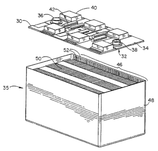
particularly to Fig. 1, there is provided a partial
illustration of an embodiment of an energy storage
module 35 which utilizes a number of rechargeable solid-
state thin-film electrochemical cells for storing
electrical energy. Such rechargeable thin-film
electrochemical cells are particularly well-suited for
use in the construction of high-current, high-voltage
energy storage modules and batteries, such as those used
to power electric vehicles for example.
As is shown in Fig. 1, the energy storage
module 35 includes a number of individual
electrochemical cells 50 which are arranged in a stack
configuration 46 and situated in a housing 48. Each of
the electrochemical cells 50 includes a pair of
electrical leads 52 disposed on opposing edges of the
cells 50. It will be appreciated that a generic stack
46 of electrochemical cells 50 may be interconnected in
various parallel and series relationships to achieve
desired current and voltage ratings. To facilitate
selective series or parallel connectivity within the
stack 46 of electrochemical cells 50, an interconnect
board 30 is situated within the housing 48.
The interconnect board 30 includes a
connection pattern or conductivity grid 32 which, when
the board 30 is installed within the housing 48,
interconnects the electrochemical cells 50 in accordance
with a pre-established connection configuration. The
connection pattern or grid 32 is typically affixed or
otherwise bonded to a sheet of insulating material 34,
CA 02297738 2000-O1-24
W O 99J05731 PCT/US98115224
7
such as a substantially rigid plastic or laminate
material. A number of electrical and electro-mechanical
components may also be mounted on the interconnect board
30.
As is shown in Fig. 1, for example, the
interconnect board 30 includes a number of fuse packs
40, equalizer and bypass devices 42, and positive and
negative power terminals 38, 36. It is understood that
any or all of the components populating the interconnect
board 30 may be mounted on boards or platforms other
than the interconnect board 30, and situated internal to
or externally of the module housing 48. In one
embodiment, the interconnect board 30 shown in Fig. 1
and the electrochemical cells 50 are disposed in a
hermetically sealed housing 48, as will further be
described with respect to Fig. 6.
As is best illustrated in Fig. 2, the
interconnect board 30 typically includes a patterned
conductive surface 32 which advantageously provides for
the interconnecting of autonomous electrochemical cells
50 in accordance with a pre-designed connection layout.
A significant advantage realized by employing an
interconnect board 30 having a patterned interconnection
surface 32 concerns the flexibility by which a desired
current and voltage rating may be achieved irrespective
of, and without disrupting, the position of individual
electrochemical cells 50 relative to one another within
the housing 48.
By way of example, and with particular
reference to Figs. 2-3, the interconnect surface 32 of
the interconnect board 30 is selectively patterned to
achieve a desired cell connection configuration. In
CA 02297738 2000-O1-24
WO 99/05731 PCT/US98/15224
8
this embodiment, the interconnect surface 32 includes a
number of electrically isolated connection regions which
are pre-designed to electrically connect with the
positive and negative contacts 52 of a particular number
of electrochemical cells 50. In accordance with this
illustrative embodiment, seven isolated connection
regions, R1-R~, are shown as constituting the patterned
interconnect surface 32 of the interconnect board 30.
When the interconnect board 30 is installed
within the housing 48 and adjacent the electrochemical
cell stack 46, the electrical contacts 52 of a first
group of electrochemical cells 50 contact the connection
region Rl at a location 54a. The opposing set of
electrical contacts 52 of the first group of
electrochemical cells 50 electrically contact the
connection region RZ at a location 54b. In this
configuration, the connection region R1 is electrically
connected to the negative power terminal 36.
A second group of electrochemical cells 50
have their respective opposing set of electrical
contacts 52 connected to connection regions R3 and Rz at
locations 56a and 56b, respectively. A third group of
electrochemical cells 50 have their respective opposing
electrical contacts 52 connected to connection regions R3
and R4 at locations 58a and 58b, respectively.
Subsequent groupings of electrochemical cells 50 have
their respective opposing electrical contacts 52
connected to connection regions R5, R6, and R~ in a
similar manner. It is noted that the connection region
R~ is electrically connected to the positive power
terminal 38.
*rB
CA 02297738 2000-O1-24
WO 99/05731 PCT/US98/15224
9
It is to be understood that any number of
connection regions of varying configuration may be
provided on the interconnect surface 32 of the
interconnect board 30. Although each of the connection
regions R1-R~ shown in Figs. 2-3 electrically communicate
with a group of electrochemical cells 50, it is
understood that a connection region may be designated to
electrically communicate with only a single
electrochemical cell 50. It can be seen that the first
l0 group of electrochemical cells 50 are connected in a
parallel relationship with respect to connection regions
R1 and R2. Similarly, the second group of
electrochemical cells 50 are connected in parallel with
respect to connection regions R3 and R2.
Having established electrical connectivity
with selected electrochemical cells 50 at selected
isolated connection regions, the connection regions are
then interconnected in a series or parallel manner
through the use of electrical conductors and/or
components. Bridging selected isolated connection
regions in this manner defines a current path the
permits current to flow through, for example, the
positive power terminal 38, each of the connection
regions R1-R~, and through the negative power terminal
36.
In one embodiment, a simple short-circuit
bridge or connector may be used to selectively
interconnect the connection regions Rl-R~ in a desired
manner to permit current to flow through the module 30.
In another embodiment, various electrical or electro-
mechanical components may be disposed on the
CA 02297738 2000-O1-24
WO 99!05731 PCT/US98/15224
interconnect board 30 which control the flow of current
between isolated connection regions.
Those skilled in the art will appreciate that
an interconnect board 30 implemented in accordance with
5 the principles of the present invention permits flexible
and selective connecting of any number of
electrochemical cells 50 in any desired series or
parallel relationship. The interconnect board 30
further permits easy integration of various control and
10 monitoring devices in series or parallel with respect to
the electrochemical cells. The interconnect surface 32
may be patterned according to various pre-designed
connection layouts to achieve desired voltage and
current ratings. The manufacturability of energy
storage modules that satisfy a wide range of power
requirements is significantly improved by, for example,
selecting among a number of interconnect boards 30
having varying interconnect surface configurations, and
installing a selected interconnect board 30 in a
selected module housing. A number of different module
housing configurations may be designed and fabricated to
house a particular number of electrochemical cells based
on the energy production requirements of a particular
application.
Turning now to Fig. 4A, there is provided a
top view illustration of one embodiment of an integrated
interconnect board 30 onto which a number of control
devices are mounted. In either of the embodiments shown
in Figs. 4A-4B, the bottom of the interconnect board
includes an interconnect surface similar in
configuration to that shown in Figs. 2-3. In the
configuration shown in Fig. 4A, the energy storage
CA 02297738 2000-O1-24
WO 99/05731 PCTIUS98/15224
11
module includes 48 individual electrochemical cells 50
grouped into six cell packs each comprising eight
parallel connected electrochemical cells 50. In the
embodiment shown in Fig. 4B, the energy storage module
includes 64 individual electrochemical cells 50 grouped
into eight cell packs each comprising eight parallel
connected electrochemical cells 50.
Associated with each of the six cell packs in
Fig. 4A is a fuse pack 40 which includes eight fuses
(not shown), with one fuse being connected in series
with one of the eight parallel connected electrochemical
cells 50 of the cell pack. The fuses within the fuse
pack 40, when activated, provide for the electrical
isolation of a defective cell from the remaining cells
of the cell pack. The interconnect board 70 shown in
Fig. 4B includes eight fuse packs 40 and also includes
temperature sensors 72 which monitor the temperature of
the interconnect board. A fuse is typically activated,
for example, upon the development of a short-circuit
within a particular cell of the cell pack.
A current bypass device may also be affixed to
the interconnect board 30/70 and connected in series
with a cell pack which, when activated, isolates a cell
pack from the series connection and bypasses current
around the defective cell pack.
An equalizer device may further be connected
in parallel with a cell pack which provides overvoltage
protection and balancing of cell pack potentials during
charging and discharging operations.
In one embodiment, the equalizer device and
bypass device are incorporated into a single integrated
component package, such as the equalizer/bypass module
CA 02297738 2006-O1-13
WO 99/05'131 PCT/US98/15224
' 12
45 shown in Fig. 4A. Additionally, a communications
device may be connected to each of the cell packs to
facilitate monitoring and controlling of individual cell
packs by an internal or external controller or
processor. Also, a temperature sensor 4?/72 may be
mounted on the interconnect board 30/70.
In Figs. 5A-5C, there is illustrated an
embodiment of an integrated equalizer/bypass module 45
which, as discussed previously, may be mounted on the
interconnect board 30/70. The integrated
equalizer/bypass module 45 advantageously provides for a
compact housing configuration capable of efficiently
dissipating heat generated during equalization and
bypass conditions through contact terminals 67, 69
affixed to the interconnect board 30/70. The heat
conducted through the contact terminals 67, 69 and to
the interconnect board 30/70 may further be conducted to
the walls of the housing 48 through thermal conductors
extending from the cells and contacting the housing
walls, as will later be discussed in greater detail.
In one embodiment, the integrated
equalizer/bypass module 45 has a total length, LT, of
2.75 inches. The housing 65 of the equalizer/bypass
module 45 has a length, LM, of 2.25 inches. The total
width, WT, of the equalizer/bypass module 45 is 1.50
inches, while the width WC of the positive and negative
terminals 67, 69 is 1.25 inches. The height, HT, of the
housing 65 is 0.625 inches, and the height or thickness,
H~, of the positive and negative terminals 67, 69 is 0.05
inches. The equalizer/bypass module 45 is mounted on
the interconnect board 30/70. The connection surface 32
of the interconnect board 30/70 includes a patterned
CA 02297738 2000-O1-24
WO 99/05731 PCTIUS98/i5224
13
copper plate having a thickness of 0.05 inches. The
thickness of the conductive sheet is required in order
to pass a relatively high current, and virtually
precludes employment of conventional photo-etched
printed circuit board (PCB) techniques.
It is noted that the heat generated by the
equalizer/bypass module 45 is typically conducted from
the integrated module 45 and interconnect board 30/70 to
the walls of the module casing 48. In accordance with
this design, the equalizer can pass a current on the
order of 5 amps which results in the generation of
approximately 15 watts of heat. Those skilled in the
art will appreciate that the high current rating of the
equalizer provides for relatively high rates of energy
storage system charging and discharging.
Returning to Figs. 2-3, one embodiment of an
interconnect board 30/70 includes a plastic sheet 34,
onto which a number of components are mounted, and a
separate sheet of electrically conductive material,
which is patterned to form an interconnect surface 32.
The patterned conductive sheet is subsequently affixed
to the plastic sheet 34. In one embodiment, the
conductive sheet constitutes a copper sheet having a
thickness of 0.05 inches and a width and length which
varies depending on the size of the module 35. The
copper sheet is machine milled to develop individual
connection regions thereon in accordance with a pre-
designed pattern layout. It is noted that the pattern
layout should be designed to minimize the volume and
weight of the copper sheet.
Following machining of the copper sheet, each
of the individual copper connection regions is cleaned
CA 02297738 2000-O1-24
WO 99/05731 PCT/US98/15224
14
and mounted to the plastic board 34 at appropriate
locations to facilitate the reconstruction of the pre-
designed pattern layout. The plastic board 34 typically
has a thickness of approximately 0.1 inches, and has a
construction similar to circuit boards commonly used
within the electronics industry. The copper connection
regions may be affixed to the plastic board 34 by
conventional adhesion or fastening techniques. It is
understood that conductive materials other than copper,
such as aluminum for example, may be employed to
fabricate the connection regions.
In an embodiment in which various electronic
devices are used to monitor and control electrical and
thermal energy generated within the module 35, such
devices are then mounted to the integrated interconnect
board 30/70. For example, a number of equalizer/bypass
modules 45 and communication devices 47 are mounted to
the interconnect board 30/70. The equalizer/bypass
modules 45 and positive and negative power terminals 38,
36 may be welded to the interconnect board 30/70, such
as by employing a known ultrasonic welding technique.
Alternatively, an air flow brazing or spot welding
technique may be employed to mount the equalizer/bypass
module 45 and terminals 36, 38 to the interconnect board
30/70.
In addition to mounting the equalizer/bypass
modules 45 and terminals 36, 38, the fuse packs 40 may
be mounted on one or both sides of the interconnect
board 30/70, depending on the cell configuration and the
need to minimize the weight and volume of the
interconnect surface 32. One side 51 of the fuse packs
is ultrasonically welded to the interconnect board
CA 02297738 2000-O1-24
WO 99/05731 PCT/US98/15224
30/70. It is noted that the use of ultrasonic welding
to mount various components to the interconnect board
30/70 results in the overall reduction in heat generated
during the welding procedure in comparison to other
5 known welding techniques. However, air flow brazing,
soldering, or spot welding techniques may be employed in
combination with well-designed heat sinks.
Finally, the interconnect board 30/70 is
mounted on the stack 46 of electrochemical cells 50.
10 Each of the cell terminals 52 is connected to the
interconnect board 30/70, which may be performed by
ultrasonic welding, soldering, or spot welding. Table 1
below provides various data associated with the use of
an interconnect board 30/70, such as that shown in Fig.
15 4A-4B, for interconnecting a number of individual
electrochemical cells 50 and various electronic devices
encased in a sealed module housing 48. The data
tabulated in Table 1 demonstrates that a total
resistance of approximately 8 micro-ohms and a total
weight of 7 to 14 grams may be realized by employing an
integrated interconnect board 30/70 of the type
illustrated herein for use in a power system capable of
passing on the order of 400 A of peak current with less
than approximately 4 mV of voltage drop across the power
terminals and a power loss on the order of 1 watt.
CA 02297738 2000-O1-24
PCTIUS98/15Z24
16
TABLE 1
MaterialThicknessVotume Weight ResistanceVolt. Power Energy
drop
Mils cube grams microohmmVolts Watts Jonles
meter @ ~C
Copper 50 1.6E-0614.41 8.39 3.36 1.34 40.29
Aluminum80 2.58E-066.94 8.64 3.46 1.38 41.48
In Fig. 6, there is illustrated an exploded
view of a power generating module 100 that includes an
inner shell 101 which contains a stack 105 of
electrochemical cells 121 and various electronic boards,
including an interconnect board 104 of the type
previously discussed. An inner shell cover 108
incorporates a hermetic seal 115, such as that described
below with respect to Figs. 7-9, that seals various
feed-throughs provided in the inner shell cover 108.
In accordance with one embodiment, the module
100 includes a stack 105 of electrochemical cells 121
which are interconnected through use of the interconnect
board 104. The stack 105 of electrochemical cells 121
are segregated into six cell packs 125, all of which are
banded together by use of two bands 127 and two opposing
end plates 129. The 48 electrochemical cells 121 are
subjected to a continuous compressive force generated by
use of the bands 127/end plates 129 and a foam or
spring-type element disposed within or adjacent each of
the cells 121. Each electrochemical cell 121 includes a
thermal conductor which is spot welded or otherwise
SUBSTITUTE SHEET (BULB 2fi)
CA 02297738 2000-O1-24
WO 99/05731 PCT/US98/15224
17
attached respectively to one or both of the positive and
negative cell contacts.
The positive and negative contacts of the
thermal conductors carry current from the cells 121 to
the interconnect board 104. The thermal conductors also
conduct heat from the cells to a metallic inner shell
101 which serves as a heat sink. The thermal conductors
include a spring portion which deforms when the cell 121
is inserted into the inner shell 101, accommodating
tolerances in cell length and changes in separation
distances between the cells 121 and the inner shell 101.
The inner shell 101 has a thickness of
approximately 1 mm and is fabricated from deep drawn
aluminum or stainless steel. The interior sides of the
inner aluminum shell 101 include an anodized coating
having a thickness of approximately 0.64 mm. The
anodized surface of the inner shell 101 provides
electrical insulation between adjacent cells 121, yet
provides for the efficient transfer of heat generated
from the cells 121 through contact with the resilient
cell conductors. In the case of a stainless steel inner
shell 101, thin plastic or mica sheet may be situated
between the cells 121 and the inner shell walls.
The interconnect board 104 is situated above
the cell stack 105 and includes control circuitry for
each of the respective six cell packs 125 constituting
the cell stack 105. Each cell pack control unit 113
includes a short circuit protection device such as a
fuse pack 107, a bypass device, and an equalizer circuit
which control the operation of the cell pack 125 while
charging and discharging. Accordingly, each of the cell
packs 125 is monitored and controlled by a respective
CA 02297738 2000-O1-24
WO 99/05731 PCT/US98/15224
18
cell pack control unit 113. A control board 10&,
situated above the interconnect board 104, includes a
processor that monitors and controls each of the six
cell pack control units 113. As such, the control board
106 provides for cell pack and module level monitoring
and control during charging and discharging operations.
A pair of quick connectors 117 pass through
corresponding holes provided in an inner shell cover 108
and serve as the main power terminals of the module 100.
The quick connectors 117 are hermetically sealed to the
inner shell cover 108 using a sealing apparatus 115.
When an outer shell cover 112 is positioned onto the
inner shell cover 108, the quick connectors 117 are
received into mating sockets 119 mounted on the
interconnect board 104. Communication connectors 111,
which pass through the inner shell cover 108 and are
similarly hermetically sealed thereto, provide external
access to the control board 106 and other electronic
boards of the module 100.
A hermetic seal is provided between the inner
shell 101 and inner shell cover 108 by welding the inner
shell cover 108 to the top of the inner shell 101. The
hermetically sealed inner shell 101 is then inserted
into an outer shell 102. The outer shell 102 may be
fabricated from glass filled polypropylene through use
of an injection molding process, and has a thickness of
approximately 2 mm. The outer shell 102 includes ribs
on three sides of the inner surface which form flow
channels when the inner shell 101 is installed in the
outer shell 102 for the purpose of transporting a heat
transfer fluid therebetween. The outer shell cover 112
may be vibration welded to the top of the outer shell
CA 02297738 2000-O1-24
WO 99/05731 PCT/US98I15224
19
102. Fluid connectors 120 are disposed on the outer
shell cover 112 and provide for the flow of heat
transfer fluid into and out of the module 100.
Referring to Figs. 7-9, there is illustrated a
hermetic seal apparatus which may be employed to provide
hermetic sealing between a conduit, such as an
electrical feed-through provided in a housing cover of a
power generating module, and a passage in the housing.
Power and communication lines, for example, may be
passed through the conduit to provide external
connectivity with power and electronic components
contained within the hermetic environment of an encased
power generating module.
The hermetic seal 220 shown in Figs. 7-9
includes a first seal body 222 having a central passage
which is in general alignment with a hole provided
through a substantially planar plate 221, such as a
cover of a power generating module housing. A second
seal body 224 of the seal 220 also includes a central
passage which is in general alignment with the hole of
the cover 221 and the central passage of the first seal
body 222. The first seal body 222 is disposed on an
upper surface of the cover 221, and the second seal body
224 is disposed on a lower surface of the cover 221.
In one embodiment, the first seal body 221
includes a collar 233 which extends through the hole of
the cover 221 and bears against an inner surface 239 of
the hole. The collar 233 includes a tapered inner
surface 238 which tapers away from the central passage
of the first seal body 222. The second seal body 224
includes a groove 235 having an inner tapered surface
CA 02297738 2000-O1-24
WO 99/05731 PCTIUS98115224
240 which tapers toward the central passage of the
second seal body 224.
As is best illustrated in the pre-sealed and
post-sealed depictions provided in Figs. 8 and 9,
5 respectively, the collar 233 of the first seal body 222
is received by the groove 235 provided in the second
seal body 224 such that the tapered surfaces 238, 240 of
the first and second seal bodies 222, 224 slidably
engage one another as the collar 233 is forced into the
10 groove 235. Engagement of the opposing tapered surfaces
238, 240 of the first and second seal bodies 222, 224 in
a fully installed configuration forces a portion 237 of
the outer surface of the collar 233 to cold flow against
the inner surface 239 of the hole provided in the cover
15 221. Those skilled in the art will appreciate that cold
flowing one material against another material forms an
extremely tight seal between the two materials. As
such, a hermetic seal is provided between the inner
surface 239 of the hole and the collar 233 through
20 slidable engagement between the collar 233 of the first
seal body and the groove 235 provided in the second seal
body 224.
As is further shown in Figs. 7-9, a conduit
226, having a first end 223 and an opposing second end
227, passes through the hole in the cover 221 and the
central passages of the first and second seal bodies
222, 224. The conduit 226 includes a central passage
through which electrical and communication lines may
pass into the internal hermetic environment of a housing
to which the cover 221 is mounted. The conduit 226
includes a flange 225 which extends outwardly from the
first end 223 of the conduit 226 and contacts a surface
CA 02297738 2000-O1-24
WO 99/05731 PCTlUS98115224
21
of the first seal body 222. The conduit 226 has a
diameter which is substantially equivalent to the
diameter of the central passages of the first and second
seal bodies 222, 224 such that an outer surface 242 of
the conduit 226 forms a tight, smooth fit with the inner
diameter surfaces of the first and second seal body
central passages.
A portion of the second end 227 of the conduit
226 is threaded so that a nut 234 may be secured
thereon. The seal 220 also includes a thrust washer 228
that abuts a lower surface of the second seal body 224.
A wave washer 230 is disposed between the thrust washer
228 and a second thrust washer 232. A nut 234, in
abutment with the second thrust washer 232, exerts an
axially directed compressive force on the elements of
the hermetic seal 220 as the nut 234 is tightened on the
threaded second end 227 of the conduit 226.
As is best seen in Fig. 9, a compressive
force, F~, produced by the tightened nut 234 causes the
wave washer 230 to compress which, in turn, forces the
inwardly tapered inner surface 240 of the second seal
body 224 into slidable engagement with the outwardly
tapered inner surface 238 of the first seal body 222.
Application of the compressive force, F~, drives the
inner diameter surface 241 of the second seal body 224
inwardly against the outer surface 242 of the conduit
226. Slidable engagement between the two tapered
surfaces 238, 240 also drives a portion 237 of the
collar 233 into tight engagement with the inner surface
239 of the hole provided in the cover 221. After
tightening the nut 234 to generate an appropriate level
of compressive force, F~, the wave washer 230 continues
CA 02297738 2000-O1-24
WO 99/05731 PCT/US98/15224
22
to apply the compressive force, F~, so as to maintain the
integrity of the hermetic seal 220 over the service life
of the seal. It is understood that the compressive
force, F~, may be produced by a fastener apparatus other
than that shown in Fig. 7, such as by use of a spring-
loaded metal keeper. Other retention devices which are
capable of maintaining a continuous compressive force,
F~, may also be employed.
In one embodiment, the cover 221 is
constructed from a metallic material, such as aluminum
or stainless steel, and the first and second seal bodies
222, 224 are fabricated from a plastic material, such as
polypropylene plastic. The conduit 226 may be
fabricated from a metallic or a plastic material. It is
noted that gaps 246, 247 may be provided in the first
and second seal bodies 222, 224, respectively, to
accommodate positional shifting between the first and
second seal bodies 222, 224 occurring from forced
engagement of the two tapered surfaces 238, 240. Also,
a notch 251 may be provided in the first seal body 222
to facilitate movement of the collar 233 in a direction
toward the inner surface of the hole of the cover 221 in
response to slidable engagement between the two tapered
surfaces 238, 240.
An alternative hermetic sealing apparatus or
feed-through is shown in Figs. 12-13. In accordance
with this embodiment, hermetic sealing is provided
primarily by an o-ring 464 which is compressed between a
flanged conductor or terminal 462 and a wall or cover
468 of the module housing. A phenolic support 466 keeps
the flanged conductor 462 at a constant distance from
the cover 468, thus creating a cavity whose dimensions
CA 02297738 2000-O1-24
WO 99!05731 PCT/US98/15224
23
are stable over time. This arrangement prevents flowing
of the o-ring material with time and high temperature.
A polypropylene ring 470 and sleeve 472
electrically insulate the bottom portion of the feed-
s through from the cover 468. In contrast to the phenolic
ring material, polypropylene maintains its high
dielectric strength even after being subjected to
arcing. It is noted that arcing typically occurs, if at
all, between the o-ring 464 and the polypropylene sleeve
472. Another advantage of using polypropylene material
for the ring 470 and sleeve 472 material is that it
provides a coefficient of friction that is sufficient to
prevent the assembly from turning when subjected to the
torque generated when wires are connected to the flanged
conductors 462. The Belleville spring 474 is flattened
when the feed-through is crimped. The Belleville spring
474 ensures that the assembly will be kept under
pressure even if the polypropylene flows over time. The
metal washer 476 helps to distribute pressure evenly
across the surface of the polypropylene ring 470.
In general, the above-described hermetic
sealing apparatuses exhibit a high dielectric strength
between the housing cover or wall and a power conductor
passing through the cover. Power terminal voltages on
the order of 2,000 V can be accommodated without
occurrences of arcing. Tight sealing (e.g., 10-8 cc-
atm/sec) is maintained even when subjected to mechanical
stresses. The hermetic seals also exhibit good torque
resistance and good overall mechanical resistance.
In accordance with one embodiment of the
present invention, the power sources shown in Fig. 6 may
constitute solid-state, thin-film cells of the type
CA 02297738 2000-O1-24
WO 99/05731 PCTIUS98/15224
24
shown in Figs. 10-11. Such thin-film electrochemical
cells are particularly well-suited for use in the
construction of high-current, high-voltage power
generating modules and batteries, such as those used to
power electric vehicles for example. In Fig. 10, there
is shown an embodiment of a prismatic electrochemical
cell 300 which includes an anode contact 301 and a
cathode current collector contact 303 formed
respectively along opposing edges of the electrochemical
cell 300.
A thermal conductor 302 is spot welded or
otherwise attached to each of the anode and cathode
contacts 301, 303, respectively. A thermal conductor
302 is typically disposed along the length of the anode
contact 301 and the cathode current collector contact
303, and typically includes an electrical connection
lead 304 for conducting current into and out of the
electrochemical cell 300, the current being collected
and conducted along the anode and cathode contacts 301,
303. The thermal conductor 302 may be fashioned from
copper and have a substantially C-shaped, double C-
shaped, Z-shaped, V-shaped, S-shaped or 0-shaped cross-
section.
In this embodiment, the electrochemical cell
300 is fabricated to have a length L of approximately
135 mm, a height H of approximately 149 mm, and a width
Wee of approximately 5.4 mm or approximately 5.86 mm when
including a foam core element. The width WC of the
cathode current collector contact 303 and the anode
contact 301 is approximately 3.9 mm, respectively. Such
a cell 300 typically exhibits a nominal energy rating of
approximately 36.5 Wh, a peak power rating of 87.0 W at
CA 02297738 2000-O1-24
WO 99/05731 PCTIUS98/15224
80 percent depth of discharge (DOD), and a cell capacity
of 14.4 Ah at full charge. Each of the electrochemical
cells 300 has a nominal operating voltage ranging
between approximately 2.0 V and 3.1 V.
5 The electrochemical cell shown in Fig. 10 may
have a construction similar to that illustrated in Fig.
11. In this embodiment, an electrochemical cell 380 is
shown as having a flat wound prismatic configuration
which incorporates a solid polymer electrolyte 386
10 constituting an ion transporting membrane, a lithium
metal anode 384, a vanadium oxide cathode 388, and a
central current collector 390. These film elements are
fabricated tv form a thin-film laminated prismatic
structure, which may also include an insulation film,
15 such as polypropylene film.
A known sputtering metallization process is
employed to form current collector contacts along the
edges 385, 383 of the anode and cathode current
collector films 384, 390, respectively. It is noted
20 that the metal-sprayed contacts provide for superior
current collection along the length of the anode and
cathode film edges 385, 383, and demonstrate good
electrical contact and heat transfer characteristics. A
spring-like thermal conductor or bus bar, such as the
25 thermal conductor 302 shown in Fig. 10, is then spot-
welded or otherwise attached to the metal-sprayed
contact. The electrochemical cells illustrated in the
Figures may be fabricated in accordance with the
methodologies disclosed in U.S. Patent Nos. 5,423,110,
5,415,954, and 4,897,917.
It will, of course, be understood that
modifications and additions can be made to the various
CA 02297738 2000-O1-24
WO 99/05731 PCT/US98115224
26
embodiments discussed hereinabove without departing from
the scope or spirit of the present invention. By way of
example, the principles of the present invention may be
employed for use with battery technologies other than
those exploiting lithium polymer electrolytes, such as
those employing nickel metal hydride (Ni-MH), lithium-
ion, (Li-Ion), and other high-energy battery
technologies. Accordingly, the scope of the present
invention should not be limited by the particular
embodiments discussed above, but should be defined only
by the claims set forth below and equivalents thereof.