Note: Descriptions are shown in the official language in which they were submitted.
CA 02297770 2004-03-01
1
INTERLEAVING SYSTEM
Technical Field
This invention relates to a method for interleaving and a device for
interleaving used in transmitters for digital telecommunications systems and
digital recording devices for recording digital data in recording media, and
this
invention also relates to a method for de-interleaving and a device for de-
interleaving used in receivers for digital telecommunications systems and
devices for reproducing digital data from recording media.
Background Art
In digital telecommunications systems that transmit digital data, signal
errors can be generated in digital data in the process of transmission, so
encoding is carried out through the use of error-correcting codes for the
digital
data to be sent.
If the number of erroneous bits in one code word is kept below a
specified value when creating these error-correcting codes, then it is
possible
to correct all of the errors at the time of error-correcting decoding on the
receiving side. The number of bits that can be corrected per code word is
known as the error correcting capacity of the error-correcting code.
Although the average code error rate itself is low in
telecommunications environments such as mobile telecommunications, burst
errors readily occur. Consequently, even if data is transmitted with error
CA 02297770 2000-01-25
F0262/3008 2
correction encoding, burst errors often occur with the number of consecutive
bits exceeding the error correcting capacity.
For this reason, the use of error-correcting codes in mobile
telecommunications environments is less effective than in telecommunications
environments where random code errors are generated. Accordingly,
interleaving is used to solve this problem.
Interleaving is a technique for scrambling the order of a bit sequence
that is to be sent, so as to transmit the bits in a sequence that differs from
the
original order.
The method of interleaving is described here with one example, using
as a unit a bit sequence of m x n bits consisting of a collection of m code
words formed from n bits. It should be noted that for the sake of convenience,
a bit sequence for one instance of interfeaving shall be referred to as a
frame.
Generally speaking, interleaving utilizes memory. In this example,
interleaving is carried out through the use of a continuous storage area of m
x
n in memory.
FIG. 20 shows this interleaving storage area expressed as a two-
dimensional memory space. The storage areas in this memory space are
specified by address data with a specified number of bits formed from a iower
address that can take n combination of values and an upper address that can
take m combination of values. In FIG. 20, storage areas with identical upper
addresses are arranged from left to right in lower address sequence, and
storage areas with identical lower addresses are arranged from top to bottom
in upper address sequence. It should be noted that hereinafter, for the sake
of convenience, a series of storage areas with identical upper addresses shall
be called rows, and a series of storage areas with identical lower addresses
shall be called columns.
When implementing interleaving, first of all, the bit sequences in
question are each to be written sequentially in their respective m x n storage
CA 02297770 2000-01-25
F0262/3008 3
area, one bit at a time. When carrying out this writing, the writing addresses
are generated by an address-generating circuit such as shown in FIG. 21, for
example. This address-generating circuit is formed from an n-scale counter
11 and an m-scale counter 12. Here, the n-scale counter 11 conducts a count
of the bit clock synchronous with the input timing of the bits that are to be
interleaved. The m-scale counter 12 increases the count value by "1" for each
nth change in the count value of the n-scale counter 11. In addition, the
writing address consisting of the count value of the n-scale counter 11 as the
lower address and the count value of the m-scale counter 12 as the upper
address is provided to the memory shown in FIG. 20, and these are written to
memory.
Consequently, as shown in FIG. 22, the code word of the initial n bit in
the bit sequence is written in the first row in the memory space, the next
code
word is written in the second row, and so forth, so that ultimately, the mth
code word is written in the mth row.
Next, the various bits that are thusly written into memory are read in an
order that differs from when they were written.
In this reading operation, a reading address is generated by the
address-generating circuit shown in FIG. 23. In the configuration shown in
FIG. 23, a count of bit blocks is conducted by an m-scale counter 22, and this
m-scale counter 22 increases the count value by "1" for each mth change in
the count value of an n-scale counter 21. In addition, the reading address
consisting of the lower address with the count value of the n-scale counter 21
and the upper address with the count value of the m-scale counter 22 is
supplied to the memory for interleaving synchronously with the bit block, and
readout of memory is implemented.
Consequently, as shown in FIG. 24, the m bits recorded in each
storage area of the first column of the memory space are read in the upper
address sequence, then the m bits recorded in each storage area of the
CA 02297770 2000-01-25
F0262/3008 4
second column are read in the upper address sequence, and so forth, so that
ultimately, the m bits recorded in each storage area of the n column are read
in the upper address sequence.
Accordingly, the bits forming the code words are distributed over the
entire area within the frame by virtue of the fact that the code words forming
the frame are written into memory, and by virtue of the fact that the bits
forming the code words are read in a sequence that differs from when they
were written. In further detail, as a result of interleaving, the n bits
forming the
code words are scattered and arranged within the frame in such a state that
they are separated by inserting them between the m-1 bits belonging to other
code words.
After implementing such interleaving, the frame is delivered to the
transmission pathway.
When the receiving side receives the frame via the transmission
pathway, a scrambling operation is executed which is the reverse of
interleaving, thereby recovering the frame with the bit sequence in the
original
order. This scrambling operation occurring on the receiving side is known as
de-interleaving.
When frames are transmitted using a transmission method that deploys
such interleaving and de-interleaving, it becomes easy to correct signal
errors
on the receiving side, even if the burst errors occur in the frames during the
transmission process.
A more detailed description is given below.
First, suppose that a burst error with a bit length of m x k occurs in an
interleaved frame during the transmission process.
Here, a burst error occurring with a bit length of m x k contains k bits
each per code word, said bits forming m code words. Accordingly, bits that
are affected by burst errors in the m code words recovered by de-interleaving
CA 02297770 2000-01-25
F0262/3008 5
are only k bits per code word. That is to say, said code error becomes a
random code error for the frame after de-interleaving.
Therefore, in cases where error correction encoding of code words is
performed through the use of error-correcting codes capable of correcting
errors numbering more than k bits, it becomes possible to correct all signal
errors on the receiving side even if burst errors occur with a bit length of m
x k.
It should be noted here that, for the sake of convenience, the effect
which is brought about by interleaving is referred to below as randomization
of
burst errors, or simply as randomization.
In cases. where the number m of code words making up a frame is
large, the number of erroneous bits per code word can .be reduced, even if
burst errors are generated that have high bit lengths. In this sense, it may
well be the case that, the greater the number m of code words making up the
frame, the greater the randomization effect imparted by interleaving.
However, since it is necessary to store at least one frame's worth of
bits in order to deploy interleaving on the transmission side and de-
interleaving on the receiving side, respectively, a delay unavoidably occurs.
Accordingly, the frame length for interleaving must be selected in such a way
as to reduce the delay. To this end, it is considered desirable to set a frame
length as an interleaving processing unit that is equal to the frame length
set
by the CODEC and the like.
Incidentally, in the case of digital transmission of data such as voice
and images, there are instances where the bit sequence forming one frame
that serves as the unit of transmission is composed of a header that has
undergone error correction encoding and a portion that has not undergone
error correction encoding. When said interleaving is executed with respect to
the entire bit sequence forming such a single frame, the following problems
occur since randomization of burst errors is also carried out on portions that
have not undergone error correction encoding.
CA 02297770 2000-01-25
F0262/3008 6
(1) Problem 1
In the case of a CODEC that handles data such as voice and the like,
when errors are predicted to occur in portions that have not undergone error
correction encoding, an operation is executed that is known as concealment,
whereby said portion is substituted into a non-sound sector. It is more
desirable that the signal errors be concentrated, so that such an operation is
executed appropriately. Thus, randomization due to interleaving is not
desirable in relation to portions that have not undergone error correction
encoding.
(2) Problem 2
In order to optimize the effect of randomization due to interleaving, it is
desirable to deploy interleaving while using as a standard the bit length n of
the code words that have undergone error correction encoding, and widely
scattering the n bits forming each code word within one frame. However, in
actual practice, different types of error correction encoding are executed,
depending on the type of data to be transmitted, and there are many cases
where one frame is formed from a plurality of types of code words (or error
correction codes). In such cases, a sufficient randomization effect can be
realized with regard to a specified error correction code when interleaving is
deployed across an entire frame using as a standard the code length of said
specified error correction code within the frame, but there arises the problem
that a sufficient randomization effect is not realized with regard to other
error
correction codes with different code lengths.
(3) Problem 3
The determination of whether randomization is advantageous or not
does not depend only on whether or not there is data that has undergone
error correction encoding. That is to say, in frames formed from bit
sequences that have undergone error correction encoding and bit sequences
that have not undergone error connection encoding, there are cases where
CA 02297770 2004-03-01
7
those bit sequences that have not undergone error correction encoding are,
by their nature, either formed in response to data which should be randomized,
or formed in response to data which should not be randomized. For each
datum forming a frame, it would be advantageous to determine whether or not
randomization is appropriate by seeking an approach that suits the nature of
the data in question, but until now, no technological means have been
provided for this purpose.
Disclosure of Invention
The present invention was devised in light of the above-.described state
of affairs, and has as its object to provide an interleaving method,
interleaving
device, de-interleaving method, and de-interleaving device which make it
possible to transmit bits that form data in a suitable configuration for said
data
by executing separate randomization for each datum forming a frame.
In order to achieve this object, the present invention provides an
interleaving method and a corresponding de-interleaving method,
characterized by scattering and arranging the bits forming bit sequences
corresponding to a second datum contained in a frame within the bit
sequence corresponding to a first datum contained within said frame to be
transmitted or recorded.
In accordance with the disclosed invention, it is possible to suitably
transmit various data, since the randomization effect due to interleaving only
extends to the second datum.
CA 02297770 2006-07-26
7a
In accordance with one aspect of the present invention there is provided
an interleaving device comprising: an operating memory configured to provide a
matrix of storage areas having columns and rows; a data writer configured to
write a first stream of bits in storage areas in the matrix, starting from a
top row of
the matrix towards a bottom thereof, in a row direction from a left most
storage
area to right; and write a second stream of bits to fill unfilled storage
areas in the
matrix, starting from a left most column to right, in a column direction from
a top
unfilled storage area of each column towards the bottom; and a data reader
configured to read the bits of the first and second streams written in the
matrix,
starting from the left most column to right, in the column direction from a
top
storage area of each column towards the bottom to output a third steam of bits
in
which the bits in the first stream are scattered into the second stream at
intervals.
In accordance with another aspect of the present invention there is
provided an interleaving method comprising the steps of: providing a matrix of
storage areas having rows and columns; writing a first stream of bits in
storage
areas in the matrix, starting from a top row in the matrix towards a bottom
thereof,
in a row direction from a left most storage area to right; writing a second
stream
of bits to fill unfilled storage areas in the matrix, starting from a left
most column
to right, in a column direction from a top unfilled storage area of each
column
towards the bottom; and reading the bits of the first and second streams
written in
the matrix, starting from the left most column to right, in the column
direction from
a top storage area of each column towards the bottom to output a third stream
of
bits in which the bits in the first stream are scattered into the second
stream at
intervals.
Brief Description of the Drawings
FIG. 1 is a block diagram showing a configuration of an interleaving device
of the first embodiment of this invention.
CA 02297770 2000-01-25
F0262/3008 8
FIG. 2 is a block diagram showing an example of a configuration of the
writing address supply part of said interleaving device.
FIG. 3 is a block diagram showing an example of a configuration of the
reading address supply part of said interleaving device.
FIG. 4 is a diagram showing the sequence of writing the bits forming a
frame at the time of interleaving into the various storage areas of operating
memory, and the sequence of reading the bits forming a frame at the time of
de-interleaving from the various storage areas of operating memory in said
embodiment.
FIG. 5 is a diagram showing the sequence of reading the bits forming a
frame at the time of interleaving from the various storage areas of operating
memory, and the sequence of writing the bits forming a frame at the time of
de-interleaving into the various storage areas of operating memory in said
embodiment.
FIG. 6 is a block diagram showing a configuration of a de-interleaving
device relating to said embodiment.
FIGS. 7A-7D are time charts showing the operation of said
embodiment.
FIG. 8 is a block diagram showing a configuration of a two-stage
interleaving device relating to the second embodiment of this invention.
FIG. 9 is a block diagram showing a configuration of a two-stage de-
interleaving device relating to said embodiment.
FIGS. 10A-10F are time charts showing the operation of said
embodiment.
FIG. 11 is a block diagram showing a general configuration of a multi-
stage interleaving device relating to said embodiment.
FIG. 12. Is a block diagram showing a general configuration of a multi-
stage de-interleaving device relating to said embodiment.
CA 02297770 2000-01-25
F0262/3008 9
FIG. 13 is a diagram describing the process of generating compressed
signal data of audio signals used by the third embodiment of this invention.
FIGS. 14A-14E are time charts showing the operadon of said
embodiment.
FIG. 15 is a block diagram showing a configuration of an interleaving
device relating to said embodiment.
FIG. 16 is a block diagram showing a configuration of a de-interleaving
device relating to said embodiment.
FIGS. 17A-17C are diagram describing the interleaving method in
Comparative Example 1 presented in contrast to said embodiment, and the
resistance to signal errors of said of said method.
FIGS. 18A-18C are diagrams describing the interleaving method in
Comparative Example 2 presented in contrast to said embodiment, and the
resistance to signal errors of said of said method.
FIGS. 19A and 19B are diagrams describing the resistance to signal
errors of the interleaving method of said embodiment.
FIG. 20 is a two-dimensional drawing illustrating the storage area of
memory used in interleaving.
FIG. 21 is block diagram showing an example of the configuration of a
device that generates writing addresses to memory during interleaving.
FIG. 22 is a diagram showing the writing sequence of bits forming a
frame into the storage area of memory during interleaving.
FIG. 23 is a block diagram showing a configuration of a device that
generates reading addresses to memory during interleaving.
FIG. 24 is a diagram showing the sequence for reading bits forming a
frame from the storage area of memory during interleaving.
Best Mode for Carrying Out the Invention
CA 02297770 2000-01-25
F0262/3008 10
Following is a description of embodiments of the present invention,
presented with reference to drawings.
A. First Embodiment
(1) The Interleaving Device
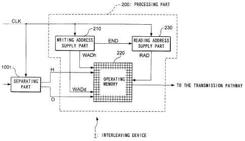
FIG. 1 is a block diagram showing a configuration of an interleaving
device 1 provided to a device on the transmission side of a digital
telecommunications system which is the first embodiment of this invention.
As shown in FIG. 1, this interleaving device comprises a separafing
part 100, and a processing part 200.
The frames that are to be transmitted to the receiving side device are
sequentially transmitted to the interleaving device 1. Each frame is a bit
sequence formed from a plurality of bits, and these bits are sequentially
supplied to the interleaving device 1 synchronously with a bit clock CLK.
When the data forming the frames are divided by category, it is
possible to distinguish between the header H and the data D which follows it.
In the example described below, the header H is formed from p bits,
and the data D is formed from m x p bits.
Furthermore, the header H undergoes error correction encoding. By
contrast, the data D does not undergo error correction encoding.
The separating part 100, is a device for separating each of the frames
that are supplied sequentially into the header H and the data D, and
outputting them. This separation can be carried out in accordance with a
method as described, for example, as follows. That is to say, the number of
bits supplied synchronously with the bit clock CLK are counted, and the
portion from the initial bit to the p bit is taken as the header H, and the
subsequent parts are taken as the data D.
The processing part 200 is a device that receives the header H and the
data D from the separating part 100õ scattering and arranging the bits forming
the header H within the data D. This processing part 200 has as its principal
CA 02297770 2000-01-25
F0262/3008 11
component elements a writing address supply part 210, an operating memory
220, and a reading address supply part 230.
Here, the operating memory 220 is a storage device for recording bits
forming the frame to be interleaved. In the present embodiment, a continuous
plurality of storage areas with addresses are selected for use from all of the
storage areas of the operating memory 220, and the various bits forming one
frame are stored in the storage areas.
Interleaving consists of the process of sequential writing of bits forming
frames to this operating memory 220, and the process of reading the bits from
this operating memory 220 in a sequence that differs from when they were
written.
The writing address supply part 210 is a device that executes a
specified address-generating program in order to generate synchronously with
the time clock CLK a writing address WADh that specifies the writing
destination of the bits forming the header H, and a writing address WADd that
specifies the writing destination of the bits forming the data D, and supplies
them to the operating memory 220, when the bits forming a frame are written
to the operating memory 220.
Furthermore, when all of the writing addresses needed for writing the
bits forming one frame into the operating memory 220 are no longer being
generated, the END signal indicating this is supplied to the reading address
supply part 230.
The reading address supply part 230 is a device that generates the
reading address RAD for reading the bits recorded in the operating memory
220, generating it synchronously with the bit clock CLK according to a
specified address-generating program when the END symbol is received, and
supplies the reading address RAD to the operating memory 220.
FIG. 2 is a block diagram showing the address-generating algorithms
of the writing address supply part 210 from the standpoint of hardware.
CA 02297770 2000-01-25
F0262/3008 12
The address-generating algorithm of this writing address supply part
210 is formed from a p-scale counter 210A, a p-scale counter 210B, an m-
scale counter 210C, an AND gate 210D, and an adder 210E. Here, the p-
scale counter 210A counts the bit clock CLK. The writing address WADh for
the bits forming the header H is a lower address with a counter value of the p-
scale counter 210A, and an upper address designated as "0".
The p-scale counter 210A stops the counting of the bit clock CLK when
the count value changes p number of times, yielding a count-over.
The AND gate 210D supplies the bit clock CLK to the m-scale counter
210C, after the p-scale counter 210A yields a count-over.
The m-scale counter 210C carries out counting of the bit clock CLK
supplied via this AND gate 210D. The count value yields a count-over when it
changes m times, but after that, as long as the bit clock CLK is supplied, the
count is repeated again from the initial value "0". The p-scale counter 210B
adds counting values "1" at a time each time the m-scale counter 210C counts
over. The adding machine 210E adds "1" to the count value of the m-scale
counter 210C.
The writing address WADd that specifies the writing destination of the
bits forming the data D is such that the count value of the p-counter 210B is
a
lower address and the output data of the adding machine 210E is an upper
address.
FIG. 3 is a block diagram showing the address-generating algorithms
of the reading address supply part 230 from the standpoint of hardware. The
address-generating algorithm of this reading address supply part 230 is
formed by a p-scale counter 230A and an (m+1)-scale counter 230B. The
(m+1)-scale counter 230B carries out counting for the bit clock CLK. The
count of the p-scale counter 230A is increased by one when the count of the
(m+1)-scale counter 230B changes m+1 times and is initialized to the initial
value "0".
CA 02297770 2000-01-25
F0262/3008 13
The read address RAD is such that the count value of this p-scale
counter 230A is a lower address, and the count value of the (m+1)-scale
counter 230B is an upper address.
The above is a detailed description of the configuration of the
interleaving device 1.
Following is a description of interleaving implemented by this
interleaving device 1, with reference to FIG. 4 and FIG. 5.
In the present embodiment, interleaving is implemented by using
(m+1) x p continuous storage areas in the operating memory 220.
FIG. 4 and FIG. 5 show the storage area of the operating memory 220
for interleaving expressed as a two-dimensional memory space. The various
individual addresses correspond to the storage areas in this memory space.
An address is formed from a lower address which can take p combinations of
values, and an upper address which can take (m+1) combinations of values.
In FIG. 4 and FIG. 5, the storage areas which are to have identical
upper addresses are arranged from left to right in lower address order, and
the storage areas which are to have identical lower addresses are arranged
from top to bottom in upper address order. As stated above, a series of
storage areas with identical upper addresses shall be called rows, and a
series of storage areas with identical lower addresses shall be called
columns.
In implementing interleaving, first of all, the bit sequences that are to be
interleaved are written sequentially, each in their respective m x n storage
areas, one bit at a time. When this writing is executed, the writing addresses
are generated by the writing address supply part 210 described above with
reference to FIG. 2.
While the p bits forming the header H are being supplied to the
operating memory 220 synchronously with the bit clock CLK, the bit clock
CLK counting is carried out according to the p-scale counter 210A in the
writing address supply part 210. The writing address WADh is generated,
CA 02297770 2000-01-25
F0262/3008 14
containing the count value of the p-scale counter 210A as a lower address,
and "0" as an upper address, and it is supplied to the operating memory 220
synchronously with the bit clock CLK.
Consequently, as shown in FIG. 4, the p bits forming the header H are
written into the initial row within the storage area of the operating memory
220
for interleaving.
Next, following the header H, the m x p bits forming the data D are
supplied to the operating memory 220 synchronously with the bit clock CLK.
In the meantime, the counting of the bit clock CLK is carried out by the
m-scale counter 210C in the writing address supply part 210, and in addition,
a count value increment of the p-scale counter 210B is executed each time
the m-scale counter 210C yields a count-over. Moreover, a writing address
WADd is generated that contains a lower address which is the count value of
the p-scale counter 210B and a upper address which is obtained by adding
the count value of the m-scale counter 210C with one, and this writing
address is supplied to the operating memory 220 synchronously with the bit
clock CLK.
Consequently, as shown in FIG. 4, the initial m bits from among the m
x p bits forming the data D are written into each storage area corresponding
to the (m+1)th row, from the second row of the first column, and into the
operating memory 220, and then the m bits are written into each storage area
corresponding to the (m+1)th row, from the second row of the second column,
and so forth, until the final m bits (i.e., the pth bit) are written into each
storage
area corresponding to the (m+1)th row, from the second column of the pth
column.
Next, the bits that are thusly written into the operating memory 220 are
read in a sequence that differs from when they were written.
In this reading operation, reading addresses are generated by the
reading address supply part 230 described with reference to FIG. 3.
CA 02297770 2000-01-25
F0262/3008 15
That is to say, the counting of the bit clock CLK is carried out by the
(m+1)-scale counter 230B, and in addition, a count value increment with a
count value of "1" only of the p-scale counter 230A is executed each time the
(m+1)-scale counter 230B yields a count-over. Moreover, a reading address
that contains the count value of the p-scale counter 230A as a lower address,
and the count value of the (m+1)-scale counter 230B as an upper address,
and this is supplied to the operating memory 220 synchronously with the bit
clock CLK.
Consequently, as shown in FIG. 5, first of all, the (m+1) bits recorded in
each storage area of the first column in the operating memory 220 are read,
.and then the (m+1) bits recorded in each storage area of the second column
are read, and so forth, untii finally, the (m+1) bits recorded in each storage
area of the pth column are read.
Due to the above-described interleaving, frames are produced such
that the p bits forming the header H are scattered and arranged at equal
intervals within the bit sequence forming the data D. It should be noted that
the state of the frames after interleaving is described in detail below with
reference to the drawings.
(2) The De-Interleaving Device
The frames that are interleaved in the transmission side device are
transmitted to the receiving side device. FIG. 6 is a block diagram showing a
configuration of the de-interleaving device 2 provided to said receiving side
device.
This de-interleaving device 2 comprises a writing address supply part
310, an operating memory 320, and a reading address supply part 330.
Here, the operating memory 320 is a storage device similar to the
operating memory 220 in the interleaving device 1. The (m+1) x p bits
forming the frames received via the transmission pathway are supplied to the
operating memory 320 synchronously with the bit clock CLK.
CA 02297770 2000-01-25
F0262/3008 16
De-interleaving consists of the process of writing these bits to the
operating memory 320, and the process of reading these bits from the
operating memory 320 in a sequence that differs from when they were written.
While the bits forming the received frame are being supplied to the
operating memory 320 synchronously with the bit block CLK, the writing
address supply part 310 supplies the writing address WAD to the operating
memory 320 synchronously with the bit clock CLK.
This writing address supply part 310 possesses a configuration
identical to that of the reading address supply part 230 in the interleaving
device 1 (see FIG. 3).
Moreover, in the case of this writing address supply part 310; the
counting of the bit dock is carried out by the (m+1)-scale counter, and in
addition, a count value increment with a count value of "1" only if the p-
scale
counter is executed each time the (m+1)-scale counter yields a count-over.
Moreover, a writing address WAD that contains the count value of the p-scale
counter as a lower address, and the count value of the (m+1)-scale counter as
an upper address is supplied to the operating memory 320 synchronously with
the bit dock.
Consequently, as shown in FIG. 5, the initial (m+1) bits from among the
(m+1) x p bits forming the received frame are written to each storage area of
the first column in the operating memory 320, and then the (m+1) bits are
written into each storage area of the second column, and so forth, until the
final (m+1) bits (i.e., the pth bit) are written into each storage area of the
pth
column.
The placement of each bit in the operating memory 320 at this time is
in agreement with the position of these bits when they are written to the
operating memory 220 of the interleaving device 1 prior to being transmitted
from the transmission side device.
CA 02297770 2000-01-25
F0262/3008 17
When the process of writing all of the bits forming the received frame to
the operating memory 320 is completed, the END signal indicating this is
supplied to the reading address supply part 330 from the writing address
supply part 310.
This reading address supply part 330 possesses a configuration
identical to that of the writing address supply part 210 in the interleaving
device 1 (see FIG. 2).
Moreover, in the case of this reading address supply part 330, the
counting of the bit clock CLK is carried out by the p-scale counter. Moreover,
a reading address RADh that contains the count value of the p-scale counter
as a lower address, and "0" as an upper address is generated, and supplied
to the operating memory 320 synchronously with the bit clock.
Consequently, as. shown in FIG. 4, the p bits forming the header H are
read from each storage area corresponding to the initial row in the operating
memory 310.
Next, in the case of the reading -address supply part 330, the counting
of the bit clock CLK is carried out by the m-scale counter, and in addition, a
count value increment with a count value of the p-scale counter is executed
each time the m-scale counter yields a count-over. Moreover, a reading
address RADd that contains a lower address which is the count value of the
p-scale counter, and an upper address which is obtained by adding the count
value of the m-scale counter with "1" is generated and supplied to the
operating memory 320 synchronously with the bit dock CLK.
Consequently, as shown in FIG. 4, the initial m bits from among the m
x p bits forming the data D are read from each storage area corresponding to
the (m+1)th row from the second row of the first column in the operating
memory 320. Then, the following m bits are read from each storage area
corresponding to the (m+1)th row from the second row of the second column
in the operating memory 320, and the following m bits are read from each
CA 02297770 2000-01-25
F0262/3008 18
storage area corresponding to the (m+1)th row from the second row of the
third column, and so forth, until the final m bits (i.e., the pth bit) are
read from
each storage area corresponding to the (m+1)th row from the second row of
the pth column.
Accordingly, the de-interleaving device 2 performs an operation that is
completely the reverse of the interleaving performed in the case of the
interleaving device 1, and restores the original un-interleaved frame.
(3) Advantageous Effects of the Present Embodiment
Following is a description of the advantageous effects of the present
embodiment, with reference to FIGS. 7A-7D.
First, FIG. 7A shows the configuration of a frame that is interleaved in
the transmission side device. As . this figure shows, the frame to be
interleaved is formed from the header H that has undergone error correction
encoding by means of an error correction code, and the data D which has not
undergone error correction encoding.
In this example, the header H consists of k1 code words, and the code
length of each code word is ml bits. Also, the header H is a bit sequence
consisting of p (= k1 x m t) bits.
The data D which has not undergone error correction encoding is a bit
sequence consisting of q (= m x p) bits.
When this frame is interleaved by means of the interleaving device 1
shown in FIG. 1, a frame is produced which has the bits arranged as shown in
FIG. 7B. That is to say, due to interleaving, the p bits forming the header H
are scattered and arranged at equal intervals within the bit sequence forming
the data D. Here, the interval after interleaving the p bits forming the
header
H is a bit length corresponding to the degree of change in the upper address
of the writing address when the each bit of the data D is written, after the
lower address of the writing address is changed in the interleaving device 1,
while writing each bit of the header H into the operating memory 220, in other
CA 02297770 2000-01-25
F0262/3008 19
words, the m bit. It should be noted here that when m=10 in FIG. 7B, the
configuration is that of a frame after interleaving.
Now let us consider the case where a burst error as the one shown in
FIG. 7C is generated in the process of transmitting a frame after the
interleaving shown in FIG. 7B. In the example shown in FIG. 7C, the second
bit in the bit sequence forming the header H and the 8'h to 15'h bits in the
bit
sequence forming the data D are compromised by the burst error.
When de-interleaving by means of the de-interleaving device 2 shown
in FIG. 6 is performed on a frame in which such burst errors have occurred,
the frames are recovered as shown in FIG. 7D.
As shown in FIG. 7D, as regards the header H in the recovered frame,
only the second bit is affected by the burst error. In an embodiment such as
this one, the header H is not readily affected by a burst error, even if said
burst error occurs in a frame in the process of transmission. Even if it were
affected, the result would be nothing more than a random error in the header
H after de-interleaving. In other words, the interleaving performed in the
present embodiment brings about the advantageous effect of randomization
of burst errors with respect to the header H.
Here, if the number of erroneous bits in the header H is within the error
correcting capacity of the error-correcting code, then the signal error can be
corrected in the receiving side device.
By contrast, as regards the data D in the recovered frame, the
continuous bits from the 8th to the 15'h bits are affected by the burst error.
Thus, in the present embodiment, when a burst error occurs in a frame in the
process of transmission, the burst error appears in the data D unchanged
after de-interleaving. That is to say, in the present embodiment, interleaving
does not bring about the effect of randomization of burst errors with respect
to
the data D.
CA 02297770 2000-01-25
F0262/3008 20
It is acceptable for the data D not to have undergone error correction
encoding in cases where the said concealment or the like have been
implemented, since the signal errors are concentrated together.
As described above, in accordance with the present embodiment, even
if a burst error occurs in the process of transmission of data D such as voice
or image to which has been added the header H that has undergone error
correction encoding, the signal error is randomized only with respect to the
header H, and the data D that has not undergone error correction encoding is
not randomized, so advantageous effects are realized in that errors relating
to
the header H are readily corrected on the receiving side, and in that it
becomes easy to implement concealment and the like on the receiving side.
(4) Variations on the Present Embodiment
Following are variations on the present embodiment which was
described above.
O In the interleaving device and the de-interleaving device, the writing
address and the reading address with respect to the operating memory
can be generated by having the processor execute specified software,
and dedicated software can be used for this purpose.
O The address-generating algorithm for interleaving is not limited to
that of the above-described embodiment. It can, for example, be the
reverse of that of the above-described embodiment in connection with
the upper addresses and lower addresses, or in connection with the
rows and columns in the operating memory. Another example is that
the header and the data can be temporarily stored in separate areas
within the operating memory, and interleaving can be performed in
connection with the present invention according to a simple method
involving the alternating repetition of single-bit reading of the bits
forming the header and m-bit reading of the bits forming the data.
CA 02297770 2000-01-25
F0262/3008 21
O In the above-described present embodiment, all bits of the header H
are written to the storage area in the space of one row in the operating
memory 220 at the time of interleaving, but it is also possible to write
into the storage space of a plurality of rows.
0 The interleaved and de-interleaved frames can have different lengths
for each frame.
O In the above-described present embodiment, the bits forming the
header are scattered and arranged within data possessing a bit length
that is greater by a factor of several integers-fold, but the ratio of the
header length and data length does not need to be in terms of integers.
In cases where the ratio of the header length and the data length
cannot be expressed in integers, it is possible to employ a method
such as performing interleaving by adding a dummy.bit to the data, with
the length of the header being expressed in terms of integers, and then
removing the dummy bit. Also, the bits forming the header do not
necessarily have to be scattered and arranged within the data at equal
intervals. If one already knows on the receiving side the method
whereby the bits forming the header will be scattered and arranged, it
is possible to perform de-interleaving on the receiving side, even if the
scattering and arranging is done at non-uniform intervals.
B. Second Embodiment
FIG. 8 is a block diagram showing a configuration of the two-stage
interleaving device 3 serving as an example of a multi-stage interleaving
device relating to the present embodiment. FIG. 9 is a block diagram showing
the configuration of a two-stage de-interleaving device 4 serving as an
example of a multi-stage de-interleaving device relating the present
embodiment. FIGS. 10A-10F are diagrams showing the operation of the
present embodiment. FIG. 11 is a block diagram showing a configuration of
an r-stage interleaving device 5 serving as a generalized example of the
CA 02297770 2000-01-25
F0262/3008 22
present embodiment. Moreover, FIG. 12 is a block diagram showing the
configuration of the r-stage de-interleaving device serving as a generalized
example of the present embodiment. As already discussed in the first
embodiment, interleaving devices are provided in transmission devices of
digital telecommunications systems, and de-interleaving devices are provided
in the equipment on the receiving side. The present embodiment is described
below with sequential reference to FIG. 8 to FIG. 12.
(1) Two-Stage Intedeaving Device
First a two-stage interleaving device 3 relating to the present invention
is described with reference to FIG. 8.
. This two-stage interleaving device 3 consists of a separating part 1002,
a processing part 200,, and a processing part 2002.
The configuration of the frame that is to be processed by the two-stage
interleaving device 3 is shown in FIG. 10A.
In the above-described first embodiment, the header H of the frame to
be interieaved was configured by a code word that had undergone error
correction encoding by only one type of error-correcting code.
A frame that is to be interleaved in the present embodiment is formed
from the header H that has undergone error correction encoding in the same
manner as in the first embodiment, and the data D that has not undergone
error correction encoding, but the header H consists of the header H, and the
header H2. Here, the header H, and the header H2 have undergone error
correction encoding according to different types of error-correcting codes. It
should be noted that for the sake of convenience in the description,
hereinafter, the bit length of the data D is to be 63 bits, the bit length of
the
header H, is to be 9 bits, and the bit length of the header HZ is to be 3
bits.
The separating part 1002 is similar to the separating part 100, relating
to the first embodiment in the sense that it divides the bit sequence forming
the frame into the header H that has undergone error correction encoding,
CA 02297770 2000-01-25
F0262/3008 23
and the data D that has not undergone error correction encoding. However,
the separating part 1002 relating to the present embodiment performs the
additional function of further separating the header H that was separated from
the data D, separating it into the header H, that has undergone error
correction encoding by a primary error-correcting code, and the header H2 that
has undergone error correction encoding by a secondary error-correcting
code.
FIG. 10B shows the header H2 and the header H, and the data D
resulting from separation by the separating part 1002.
In addition, the separating part 1002 supplies the data D and the
header H, to the processing part 200,, and supplies the header HZ to the
processing part 2002. The processing results of the processing part 200, are
also delivered to the processing part 2002, along with the header H2.
The processing part 200, and the processing part 2002 both possess
almost the same configuration as the processing part 200 of the first
embodiment.
Moreover, the processing part 200, performs interleaving, which
scatters and arranges the 9 bits that make up the header H, in the bit
sequence of the data D. The configuration and operation for performing
interleaving have already been described in the first embodiment, with
reference to FIG. 1 to FIG. 5.
FIG. 10C shows a bit sequence output by the processing part 200, in
the process of interleaving.
As shown in FIG. 10C, the 9 bits making up the header H, are
scattered and arranged at equal intervals in the but sequence making up the
data D, said bit sequence consisting of 72 (= 8 x 9) bits output by the
processing part 200,. Here, 7 (= 63/9) continuous bits in the data D are
inserted between the bits making up the header H,. The bit sequence of the
data D inserted between the bits of the header is 7 bits.
CA 02297770 2000-01-25
F0262/3008 24
Next, the processing part 2002 executes interleaving, thereby scattering
and arranging the 3 bits making up the header HZ at equal intervals within the
72-bit bit sequence output by the processing part 200,. The details of the
processing involved in the interleaving performed by this processing part 2002
is identical to that of the interleaving performed by the processing part
200,.
FIG. 10D shows a bit sequence as it passes through the process of
interleaving performed by the processing part 2002.
As shown in FIG. 10D, in the bit sequence after interleaving, 24
72/3) continuous bits in the bit sequence output by the processing part 200,
are inserted among the 3 bits forming the header H2.
The bit sequence produced by the processing part 2002 is sent to the
receiving side device via the transmission pathway as a frame that has
undergone two-stage interleaving.
(2) Two-Stage De-Interleaving Device
Following is a description of the two-stage de-interleaving device 4
provided to the receiving side device.
As shown in FIG. 9, the two-stage de-interleaving device 4 consists of
a processing part 3002, a processing part 300,, and a synthesizing part 4002.
The processing parts 300, and 3002 both possess a configuration
similar to the de-interleaving device 2 in the first embodiment (see FIG. 6).
The processing part 3002 performs de-interleaving on the frames
received from the transmission pathway, by an operation that is the complete
reverse of the interleaving performed by the processing part 2002.
For example, in the case where a frame with the content shown in FIG.
10D is delivered to the processing part 3002, the bit sequence shown in FIG.
10C is obtained by the de-interleaving performed by the processing part 3002.
This bit sequence consists of the bit sequence of 3 bits forming the
header H2, and the bit sequence with the bits forming the header H, scattered
and arranged in the bit sequence of the data D.
CA 02297770 2000-01-25
F0262/30Q8 25
Of these, the header H2 is supplied to the synthesizing part 4002. On
the other hand, the bit sequence of bits forming the header H, scattered and
arranged in the bit sequence of the data D is supplied to the processing part
300,.
The processing part 300, performs de-interleaving, which is the
completely reverse operation from the interleaving performed by the
processing part 200,. Due to this de-interleaving, the data D, formed from the
header H, consisting of 7 bits plus the 63 bits shown in FIG. 10B, is
recovered
from the bit sequence of the bits forming the header H, scattered and
arranged in the bit sequence of the data D.
The synthesizing part 4002 synthesizes the header H2 and the header
H, with the data D, outputting the original frame shown in FIG. 10A.
The above is a detailed description of the two-stage de-interleaving
device 4 shown in FIG. 9.
(3) Advantageous Effects of the Present Embodiment
Following is a description of the advantageous effects of the present
embodiment, with reference to FIGS. 10A-10F.
First, let us suppose that the burst error shown in FIG. 10E is
generated in the process of transmission of the interleaved frame shown in
FIG. 10D. In the example shown in FIG. 10D, 1 bit in the bit sequence
forming the header H,, 1 bit in the bit sequence forming the header H2, and
several continuous bits forming the data D are compromised by the burst error.
When the frame that has been affected by such a burst error is
received by the receiving side device, and then de-interleaved by the two-
stage de-interleaving device 4, the frame is recovered in the state shown in
FIG. 10F.
In the recovered frame, the effect of the burst error is manifested in the
header H, that has undergone error correction encoding by the primary error-
correcting code and in the header H2 that has undergone error correction
CA 02297770 2000-01-25
F0262/3008 26
encoding by the secondary error-correcting code, resulting in a random signal
error of 1 bit each, and the effect of the burst error is manifested in the
data D
that has not undergone error correction encoding, resulting in a signal error
of
several continuous bits. That is to say, in the present embodiment, the
advantageous effect of randomization by interleaving affects only the header
H, and the header H2, but the advantageous effect of randomization due to
interleaving does not affect the data D.
Here, if the number of erroneous bits in the headers H, and H2 is within
the error correcting capacity of the error-correcting codes, the erroneous
bits
can be corrected. Furthermore, the aforementioned concealment is
implemented since burst errors occur in the data D that has not undergone
error correction encoding.
As described above, in accordance with the present embodiment, and
as in the above-described first embodiment, errors are randomized only with
respect to the headers H, and H2, even if burst errors are generated in the
process of transmitting the added headers H, and H2 that have undergone
error correction encoding by two different error-correcting codes to data D
such as voice and images, but errors are not randomized with respect to the
data D. Therefore, error correction for the headers is readily accomplished on
the receiving side, and there is also the advantageous effect that concealment
and the like is readily implemented on the receiving side with respect to the
data D. Furthermore, since interleaving is executed twice by scattering and
arranging the bits in the header H, and H2 in the present embodiment, it is
possible to achieve the advantageous effect of maximum randomization for
each header, by performing interleaving under the optimal conditions for each
head.
(4) General Configuration of a Multi-Stage Inte-rleaving Device and a
Multi-Stage De-Interleaving Device
CA 02297770 2000-01-25
F0262/3008 27
The above describes the case where the header that has undergone
error correction encoding consists of two components, namely, the header H,
that has undergone error correction encoding by the primary error-correcting
code, and the header HZ that has undergone error correction encoding by the
secondary error-correcting code, but the present embodiment is not limited to
this case, and can, of course, be applied also to the case where the frame
possesses 3 or more headers that have undergone error correction encoding
by different error-correcting codes.
FIG. 11 shows the configuration of the r-stage interleaving device 5
which interleaves frames that contain r number of headers that have
undergone error correction encoding by different error-correcting codes.
As shown in the figure, the r-stage interleaving device 5 consists of the
separating part 100õ and the r number of processing parts 200, - 200,.
The separating part 100, divides the frame into the r number of headers
H,-H,andthedataD.
The processing part 200, executes interleaving which scatters and
arranges the bits forming the header H, at equal intervals in the bit sequence
forming the data D, and outputs the resulting bit sequence.
The processing part 2002 executes interleaving which scatters and
arranges the bits forming the header H2 at equal intervals in the bit sequence
output by the processing part 200,.
The same applies to the other processing parts as well. That is to say,
the various processing parts 200k (where k= 1 to r) in FIG. 11 execute
interleaving which scatters and arranges the bits forming the headers Hk at
equal intervals in the bits output by the processing part 200k_1.
Then, the bit sequence obtained from the final stage (the rth stage)
processing part 200, is transmitted to the receiving side device via the
transmission pathway as an interleaved frame.
CA 02297770 2000-01-25
F0262/3008 28
De-interleaving of the received frame is performed in the receiving side
device, by means of an r-stage de-interleaving device 6 shown in FIG. 12.
This r-stage de-interteaving device 6 possesses an r number of
processing parts 300k (where k = 1 to r) and the synthesizing part 400,.
The processing parts 300k (where k = 1 to r) execute de-interleaving,
which is completely the reverse operation from the interleaving performed by
the processing parts 200k (where k = 1 to r).
In further detail, the processing parts 300k perform de-interleaving,
which is the reverse of the interleaving performed by the processing parts
200k, on the frames received in the process of transmission, and it also
outputs the header H, formed from continuous bits, and a bit sequence with
the bits forming other headers scattered and arranged within the data D. In
addition, the processing parts 300k deliver the headers H, to the synthesizing
part 400,, and deliver the latter bit sequence to the processing part 300,,.
Next, the processing part 300,_, performs de-interleaving on the bit sequence
output by the processing part 300,, the reverse of the interleaving performed
by the processing part 200k-,, and outputs the header H,., formed from
continuous bits, and a bit sequence with the bits forming other headers
scattered and arranged within the data D. Furthermore, the processing part
300r, delivers the header H~, to the synthesizing part 400, and delivers the
latter bit sequence to the processing part 300,.2. The various processing
parts
300k following this processing part 300,.2 also perform the same operation.
Then, the processing part 300, of the final stage performs de-interleaving,
which is the reverse of the interleaving performed by the processing part
200,,
with respect to the bit sequence output by the processing part 3002, and
delivers both the header H, and the data D to the synthesizing part 400,.
The synthesizing part 400, synthesizes the headers H, - H, output by
the various processing parts and the data D, thereby recovering the original
frame.
CA 02297770 2000-01-25
F0262/3008 29
It is clear from the above description that the present invention can be
applied not only to the case where a frame has two types of headers, but also
to the case where a frame has 3 or more types of headers.
C. Third Embodiment
In the first and second embodiments, the frame to be transmitted is
separated into the part that has undergone error correction encoding and the
part that has not undergone error correction encoding, and interleaving is
performed by scattering and arranging the bits making up the former across
the entire range of the bit sequence of the latter.
Embodiments of interleaving in the present invention are not limited to
the above.
For example, there is the case where data that has not undergone
error correction encoding contain types of data strings that, because of their
nature, should undergo the randomization effect of interleaving.
The present embodiment assumes this type of case. In the present
embodiment, the data that has not undergone error correction encoding is
divided into a part for which the randomization effect of interleaving is
desirable, and a part for which it is not desirable, and interleaving is
performed by scattering and arranging the bits that make up the former part in
the bit sequence of the latter part.
Compressed signal data of audio signals are suitable objects for
application of the present embodiment. Before describing the process of
interleaving in the present embodiment, there follows an explanation of the
method for generating such encoded data, making reference to FIG. 13.
First, a Modified Discrete Cosine Transformation (MDCT), a type of
time-frequency transformation, is performed on a single-frame audio signal
sample (1,024 samples in this example), thereby converting the audio signal
to parameters on the frequency axis known as MDCT coefficients.
CA 02297770 2000-01-25
F0262/3008 30
Next, the MDCT coefficients are divided into previously-determined
frequency band (scale factor band) units. Since the frequency resolution is
typically narrower than the band width of this scale factor band, a plurality
of
MDCT coefficients will be present in each scale factor band.
Next, for each of the scale factor bands, the scale factor SF and the
spectral data ML are derived from the plurality of MDCT coefficients X. Here,
the scale factor SF corresponds to an indicator when the MDCT coefficient is
discript as a floating point, and the spectral data ML corresponds to a
parameter.
A plurality of MDCT coefficients belong to each scale factor band, but
the scale factor SF is generated one at a time for each scale factor band. On
the other hand, the spectral data ML are generated in response to the various
MDCT coefficients X belonging to said scale factor bands.
The relationship among the above-described MDCT coefficient X, the
scale factor SF, and the spectral data ML is given by the following formula:
Abs(X) = int((abs(ML)*(2"(1/4*(SF-OFFSET))))"(3/4)+MAGIC NUMBER)
......(1)
However, in the formula above, the function abs(X) represents the
absolute value of the variable X. Also, OFFSET and MAGIC NUMBER are
constants, e.g., OFFSET=100 and MAGIC NUMBER=0.4054.
According to Formula (1), multiple combinations of the scale factor SF
and the spectral data ML can be obtained with respect to one MDCT
coefficient X. Thus, there is some freedom in the selection of the scale
factor
SF. Accordingly, the scale factor SF is selected so as to reduce to a minimum
the amount of data of the spectral data ML corresponding to each MDCT
coefficient belonging to the scale factor band in question. This scale factor
SF
is obtained by iteration, through repeated calculations of Formula (1).
CA 02297770 2000-01-25
F0262/3008 31
Next, differential encoding of each scale factor SF corresponding to
each scale factor band is carried out.
First, in the case where the scale factor band is, for example, from
band 1 to band n, the differential between the scale factor SF of band 1 and
the scale factor SF of band 2, the differential between the scale factor SF of
band 2 and the scale factor SF of band 3, are determined, and so forth, until
the differential of the scale factor of band n-1 and the scale factor SF of
band
n is determined.
Next, the resulting differentials are encoded using a Reversible
Variable Length Code (RVLC). This RVLC is a reversible variable length
code from the front as well as from the back.
An example of this RVLC is a variable length code containing a fixed
number of "1 ". For example, if the number of "1 "s is determined in advance
to
be "3" then it is possible to generate a series of RVLC such as "111 ", "1011
",
"1101 ", "11001 ", and "10101".
In another example, variable length codes containing an equal number
of "0" and "1 " can form a RVLC (e.g., "01 ", "10", "0011 ", "1100", "001011",
"000111", "110100", etc.). There is also the example of RVLC where the code
is completely symmetrical right/left (e.g., "0", "101 ", "111", "1001 ",
"11011 ",
"10001", etc.) .
Regarding the spectral data ML, Huffman encoding is performed, and
Huffman code scrambling is executed. When this Huffman code scrambling is
executed, it is possible to prevent errors from propagating at the time of
decoding.
Next, using the resulting data, a frame is assembled consisting of the
header H, the data D, corresponding to the scale factor SF, and the data D2
corresponding to the spectral data ML.
In this frame, the header H includes a code word that has been
obtained by carrying out error correction encoding on important information
CA 02297770 2000-01-25
F0262/3008 32
such as effective scale factor bands and various scale factors SF in band 1
and n. Here, the various scale factors SF in band 1 and n are utilized as the
initial scale gain data when undertaking consecutive decoding of the scale
factor SF of each band in the receiving side device. The reason why this
initial scale gain data and error-correcting encoding for the number of scale
factor bands are included in the header H is that if it is impossible to
correctly
decode these data in the receiving side device, then decoding of all scale
factors SF belonging to the frame becomes impossible.
The data D, contains RVLCs encoded with the differentials between
the scale factors SF of the various bands. The data D2 contains data for
which the spectral data ML has undergone Huffman encoding as well as
Huffman code scrambling. It should be noted that the data D, and D2 have
not undergone error correction encoding.
To sum up the above points, frames that are suitable for use in the
present embodiment are as follows:
a. Error correction encoded header H
Initial scale gain data (various scale factors SF in band 1 and n)
Effective number of scale factor bands
b. Error correction unencoded data D,
RVLC encoded with differentials between the scale factors SF of the
various bands
c. Error correction unencoded data D2
Data with Huffman encoded spectral data ML and that has undergone
Huffman code scrambling
The number of bits of the header H, and the data D, and D2 varies from
frame to frame, but, under conditions such as a sampling rate of 40 kbps/48
kHz, for example, the number of bits will be on the order of 320 bits, 80
bits,
and 1,200 bits, the order shown in FIG. 14A.
CA 02297770 2000-01-25
F0262/3008 33
The above is a detailed description of the object to be transmitted in
the present embodiment.
FIG. 15 is a block diagram showing the configuration of an interleaving
device relating to the present embodiment where interleaving is performed on
such an object.
As shown in the figure, the interleaving device relating to the present
embodiment consists of a separating part 1003i plus the two processing parts
2003 and 2004.
Of these, the separating part 1003 is similar to the separating part 100,
of the first embodiment, in the sense that one frame is divided into the
header
H that has undergone error correction encoding, and data which has not
undergone error correction encoding. However, the separating part 1003
relating to the present embodiment separates the data that has not undergone
error correction encoding further into the data D, corresponding to the scale
factor SF, and the data DZ corresponding to the spectral data ML. In addition,
the separator part 1003 delivers the header H to the processing part 2004, and
the data D, and D2 to the processing part 2003.
The configurations of the processing parts 2003 and 2004 are almost
identical to that of the processing part 200 of the first embodiment.
Moreover, the processing part 2003 performs interleaving by scattering
and arranging the bits forming the data D, in the bit sequence of the data D2,
so that the resulting bit sequence is output.
The processing part 2004 performs interleaving by scattering and
arranging the bits forming the header H at equal intervals across the entire
range of the bit sequence output by the processing part 2003, and after this
interleaving, the frame is delivered to the receiving side device via the
transmission pathway.
CA 02297770 2000-01-25
F0262/3008 34
Next, a specific example of the operation of an interleaving device
relating to the present embodiment is explained with reference to FIGS. 14A-
14E.
First, the content of the frame to be transmitted is as already seen for
reference in FIG. 14A.
As shown in FIG. 14B, this frame is separated into the header H, the
data D,, and the data D2. In this example, the header has 320 bits, the data
D, has 80 bits, and the data D2 has 1,200 bits.
As shown in FIG 14C, interleaving is performed by the processing part
2003 by scattering and arranging the 80 bits forming the data D, at equal
intervals in the bit sequence of 1,200 (15 x 80) bits forming the data D2,
using
a continuous storage area of 80 x(15+1) bits in the operating memory.
This storage area for interleaving is represented two-dimensionally in
FIG. 14C.
First, as shown in FIG. 14C, the 80 bits forming the data D, are written
to a storage area of 80 units corresponding to the first row of the operating
memory.
Next, the initial 15 bits in the data DZ are written in the 15-unit storage
area corresponding to rows 2-16 of the first column of the operating memory,
and the next 15 bits are written in a 15-unit storage area corresponding to
rows 2-16 of the second column, and so forth, until the final (i.e., the 801h)
15
bits are written in a 15-unit storage area corresponding to rows 2-16 of the
80' column.
Then, 16 bits are read from each storage area corresponding to rows
1-16 of the first column of the operating memory, and 16 bits are read from
each storage area corresponding to rows 1-16 of the second column, and so
forth, until the final 16 bits are read from each storage area corresponding
to
rows 1-16 of the 80'h column.
CA 02297770 2000-01-25
F0262/3008 35
Accordingly, as shown in FIG. 14D, the bits forming the data D, are
scattered and arranged in equal intervals in the bit sequence of the data D2,
yielding a bit sequence of 1,280 bits, which is output to the processing part
2004.
The processing part 2004 performs interleaving by scattering and
arranging the 320 bits forming the header H at equal intervals within the
1,280
(4 x 320) bits output by the processing part 2003.
Interleaving by the processing part 2004 yields the bit sequence of
1,600 bits shown in FIG. 14E.
This bit sequence is transmitted to the receiving side device as a frame
after interleaving.
The above is a detailed description of an interleaving device relating to
the present embodiment.
De-interleaving of received frames is executed by the receiving side
device, using the de-interleaving device shown in FIG. 16.
This de-interleaving device consists of the two processing parts 3004
and 3003, and the synthesizing part 4003.
The processing parts 3003 and 3004 each possess the same
configuration as the de-interieaving device 2 (see FIG. 6) of the first
embodiment. The synthesizing part 4002 has the same function as the
synthesizing part 4002 of the second embodiment.
De-interleaving of the received frame is performed by this de-
interleaving device, yielding the header H, the data D,, and the data D2 with
their bits arranged in their original sequence.
The reproduction of audio signals is also carried out based on the
header H, the data D,, and the data D2.
Specifically, first, the data needed for decoding, such as the initial scale
factor gain data (scale factors SF of bands 1 and n) and the effective scale
factor band number, are taken from the header H.
CA 02297770 2000-01-25
F0262/3008 36
Next, the differential between the scale factors SF of the various bands
is determined from the various RVLC contained in the data D,, and the scale
factor SF for each band 1-n is decoded, using these differentials and the
initial
scale factor gain data. In this case, since decoding from low frequency to
high frequency and decoding from high frequency to low frequency are both
possible, the scale factor SF of a large number of bands can be decoded,
even when signal errors occur in either type of RVLC.
That is to say, if, for example, the differential needed to determine the
scale factor SF for the high-frequency bands n-1 cannot be obtained due to a
signal error, then the scale factor SF of band 2 is determined by adding the
differential between the scale factors for bands 1 and 2 to the scale factor
SF
(initial scale gain data) of band. 1, after which the scale factor SF of band
3 is
determined by adding to the aforementioned sum the differential of the scale
factors of band 2 and 3, and so forth, so as to determine the scale factors SF
for all for all bands, from the low-frequency side to the high-frequency side.
By contrast, in cases where, for example, the differential needed to determine
the scale factor SF of the low-frequency band 2 cannot be obtained due to a
signal error, the differential between the scale factors of band n-1 and n is
subtracted from the scale factor SF (initial scale gain data) of band n, after
which the scale factor SF of the band n-3 is determined by subtracting the
differential between the scale factors of band n-3 and n-2 from the
aforementioned result of subtracfion, and so forth, so as to determine the
scale factors SF for all bands, from the high-frequency side to the low-
frequency side.
Next, the scale factors SF for the various bands and the spectral data
ML for the various MDCT coefficients of the bands included in the data D2, are
substituted into Formula (1) above, so as to regenerate the various MDCT
coefficients X belonging to the bands.
CA 02297770 2000-01-25
F0262/3008 37
Moreover, in cases where the scale factor SF cannot be decoded due
to a signal error, concealment is implemented on the band corresponding to
the scale factor SF. In other words, the spectral data ML is set at "0" in
relation to said band.
Next, in addition to implementing reverse MDCT conversion on the
MDCT coefficient X, the audio signal is regenerated based on the results of
the reverse MDCT conversion and the header data.
The above is a description of the operation of the receiving side device.
A description of the advantageous effects of the present embodiment
follows.
In order to more properly understand the advantageous effects of the
present embodiment, first of all, a comparative example will be provided
describing an interleaving method other than the interleaving method of the
present embodiment, and an explanation of resistance to signal errors is
provided for the case where this method is employed. After that, a
comparison will be made with the present embodiment, and an explanation of
resistance to signal errors is provided for the case where the present
embodiment is employed.
First is given Comparative Example 1, which is an interleaving method
other than that of the present embodiment. As in the above-described first
embodiment, the case is considered where the bits forming the header H that
has undergone error correction encoding are scattered in the bit sequence
corresponding to both the data D, and D2 that have not undergone error
correction encoding. It should be noted that for the sake of convenience in
making a comparison with the present embodiment, the header H shall have a
bit length of 320 bits, the data D, shall have a bit length of 80 bits, and
the
data D2 shall have a bit length of 1,200 bits.
CA 02297770 2000-01-25
F0262/3008 38
As shown in FIG. 17A, interleaving in this case is performed using a
continuous storage area of 320 x (1200 + 1) units in the operating memory.
FIG. 17A is a two-dimensional representation of the storage area used
for interleaving.
First, as shown in FIG. 17A, the 320 bits forming the header H are
written to the 320 units of storage area corresponding to the first row of the
operating memory.
Next, the initial 4 bits in the data D, are written to the 4 units of storage
area corresponding to rows 2-5 of column 1 of the operating memory, then the
next 4 bits are written into the 4 units of storage area corresponding to rows
2-
5 of column 2, and so forth, until the final 4 bits are written to the 4 units
of
storage area corresponding to rows 2-5 of column 20.
Accordingly, once writing of the 80 bits forming the data D, is finished,
writing of the 1,200 bits forming the data DZ is then executed. That is to
say,
the initial 4 bits in the data D2 are written to each storage area
corresponding
to rows 2-5 of column 21, the next 4 bits are written to each storage area
corresponding to rows 2-5 of column 22, and so forth, until the final 4 bits
are
written to each storage area corresponding to rows 2-5 of column 320.
Thus, once the writing of the bits forming the header H, the data D,,
and the data D2 to the operating memory is finished, the bits stored in the
operating memory are read in an order that differs from when they were
written. That is to say, 5 bits are read from each storage area corresponding
to rows 1-5 of column 1 of the operating memory, then 5 bits are read from
each storage area corresponding to rows 1-5 of column 2, and so forth, until
the final 5 bits are read from each storage area corresponding to rows 1-5 of
column 320.
Accordingly, the 320 bits forming the header H are scattered and
arranged at equal intervals in the 1,280-bit bit sequence forming the data D,
CA 02297770 2000-01-25
F0262/3008 39
and the data D2, resulting in a bit sequence of 1,600 bits, which is
transmitted
to the receiving side device via the transmission pathway.
Let us suppose that a burst error occurs in the process of transmission,
as shown in FIG. 17B. In the example depicted in FIG. 17B, the 5 bits from
the 9'h to the 13'h bit of the 320 bits forming the header H, plus several
continuous bits forming the data D, are compromised by a burst error.
Here, in connection with the header H, randomization is implemented
through interleaving, and the effect of the burst error is manifest in the
form of
random signal errors. Therefore, as long as the number of erroneous bits [4
bits in the example shown in FIG. 17B] is within the error correcting
capacity,
the signal error can be corrected in the receiving side device.
At the same time, in the example shown in FIG. 17B, the data D,,
which includes the RVLC needed to sequentially determine the scale factor
SF of each band, is compromised by a burst error.
Here, the MDCT coefficient X for each scale factor band is generated,
based on the spectral data ML and scale factor SF recovered by the receiving
side device. Therefore, when a burst error occurs in either the data D, or in
the data D2, it becomes impossible to decode the scale factor band
corresponding to the erroneous part, even if there are no errors in the other.
Moreover, in the example depicted in FIG. 17B, an error has occurred
in the bit sequence of the data D,, that is to say, in the continuous bit
sequence from the 19"' bit to the 38' bit of the bit sequence of the RVLC
needed to determine the scale factor SF of each band. Thus, the entire scale
factor band that needs the RVLC where the signal error occurred for decoding
the scale factor SF becomes an undecodable sector. As shown in FIG. 17B,
when an error occurs in a large number of bit sequences among the RVLC bit
sequence, a decodable period arises that includes a large number of bands,
as shown in FIG. 17C.
CA 02297770 2000-01-25
F0262/3008 40
Comparative Example 2 will now be described. In this Comparative
Example 2, interleaving is performed on a frame by means of an interleaving
device of the type shown in FIG. 15. However, the interleaving performed
according to this Comparative Example 2, differs from the interleaving
performed according to the present embodiment.
In this Comparative Example 2, as shown in FIG. 18A, the processing
part 2003 writes the 80 bits forming the data D, needed to decode the scale
factor SF, dividing them into 40 bits each for row 1 and row 2 of the
operating
memory. Next, the processing part 2003 writes the initial 30 bits of the 1,200
bits forming the data D2 to each storage area covering row 3 to row 32 of
column 1 of the operating memory, and then writes the next 30 bits to each
storage area covering row 3 to row 32 of column 2, and so forth, until writing
the final 30 bits to each storage area covering row 3 to row 32 of column 40.
Then, once this writing is completed, the processing part 2003 reads 32 bits
from each storage area from rows 1-32 of column 1, then reads the 32 bits
from each storage area from rows 1-32 of column 2, and so forth, until the
final 30 bits are read from each storage area from rows 1-32 of column 40.
Then, the processing part 200, delivers to the processing part 2004 a bit
sequence of the 1,280 bits that were read in the described manner.
Next, the processing part 2004performs interleaving by scattering and
arranging the 320 bits forming the header H at equal intervals in the bit
sequence of the 1,280 bits output from the processing part 2003.
FIG. 18B shows the configuration of a bit sequence resulting from this
interleaving.
This bit sequence is transmitted to the receiving side device as an
interleaved frame.
In the process of transmitting this frame, a burst error occurs as shown
in FIG. 18B.
CA 02297770 2000-01-25
F0262/3008 41
In the example depicted in FIG. 18B, the 3rd bit, 4th bit, 43rd bit, and
4411 bit of the data D, needed for decoding the scale factor SF, are
compromised by the burst error. The scale factor bands that cannot decode
the scale factor SF due to these bit errors form an undecodable sector.
Incidentally, an RVLC is used to encode the scale factor SF, and the
scale factor SF corresponding to band 1 with the lowest frequency and the
scale factor SF corresponding to band n with the highest frequency are
included in the header H as initial spectral gain data. Therefore, when a
signal error occurs in the RVLC corresponding to a high frequency band,
decoding is carried out from low frequency toward high frequency, and
conversely, when signal errors occur in RVLC corresponding to low-frequency
bands, the scale factor SF of a very wide range of bands can be recovered by
decoding from high frequency toward low frequency.
However, when interleaving is performed as described above out by
writing the bits forming the data D, to each storage area corresponding to a
plurality of rows in the operating memory, the bits forming each RVLC needed
to decode the scale factor SF in the frame after interleaving appear as 2
continuous bits [see FIG. 18B]. Accordingly, there is an increase in the
number of bits compromised by the burst error among the bit needed to
decode the scale factor SF. Moreover, it is highly probable that the various
RVLCs corresponding to 2 or more bands that are separated on the frequency
axis among the component bits of the various RVLCs needed to decode the
scale factor SF will be compromised by the burst error.
In addition, when a signal error occurs in the component bits of the
various RVLCs corresponding to a plurality of bands separated on the
frequency axis, the sector from the band with the lowest frequency to the
band with the highest frequency becomes an undecodable sector, as shown
in FIG. 18C.
CA 02297770 2000-01-25
F0262/3008 42
In contrast to Comparative Examples 1 and 2, the present embodiment
is able to scatter the component bits of the RVLC needed to decode the scale
factor SF, arranging them at equal intervals in the frame, since all bits
forming
the data D, corresponding to the scale factor SF are written to the first row
of
the operating memory, when interleaving is performed in the processing part
2003. Furthermore, the component bits of the RVLC needed to decode the
scale factor SF of each band have the same sequence as the sequence of
each band on the frequency axis, appearing in the bit sequence after
interleaving. Therefore, even if a burst error such as shown in FIG. 19A
occurs in a frame during transmission, nothing more will happen than that it
will be impossible to decode the scale factor SF corresponding to the
neighboring band on the frequency axis. It is therefore possible to shorten
undecodable sectors accompanying a loss of the scale factor SF, as shown in
FIG. 19B.
In accordance with the present embodiment, in cases where there is a
header H that has undergone error correction encoding, and the data D, and
D2 that have not undergone error correction encoding, the bits for decoding
the scale factor SF contained in the data D, are scattered and arranged in the
data D2, and moreover, the bits forming the header H are scattered and
arranged in the resulting bit sequence, so that even if a burst error occurs,
it is
possible to reduce the probability that the scale factor SF will become
undecodable, thereby enhancing the quality of the reproduced audio signals.
Moreover, since the various bits are written only into the first row of the
operating memory when the bits needed for decoding the scale factor SF are
scattered and arranged, the bits needed to decode the scale factor SF of the
various bands are scattered and arranged in the frame in an order identical to
the order of the bands on the frequency axis.
Therefore, even if a burst error occurs, it is possible to concentrate on
the frequency axis the scale factor SF that can get lost. Thus, undecodable
CA 02297770 2000-01-25
F0262/3008 43
bands can be concentrated into a very narrow range. As a result, the quality
of the reproduced audio signals can be enhanced.
D. Variations on the Above-Described Embodiments
The interleaving device and de-interleaving device relating to
embodiments 1-3 can be realized with the depicted hardware configuration, or
with a software configuration for executing a program for am operation similar
to the one described above.
Furthermore, in the above-described embodiment, bits forming the
header H that had not undergone error correction encoding were scattered,
arranging them in a bit sequence of data that had not undergone error
correction encoding, but the present invention is not limited to this, and the
above-described interleaving and de-interleaving can, of course, also be
applied to parts that have not undergone error correction encoding.
Also, in the third embodiment, an example was given of the case where
the present invention was applied to 3 parameters that represent 1 signal, but
the present invention is not limited thereto, and it is of course also
permitted
for 1 signal to be represented by 4 or more parameters. In this case,
interleaving can be performed by scattering and arranging the bits
corresponding to some parameters in a bit sequence corresponding to one of
the remaining parameters, and performing multiple repetitions of this
scattering corresponding to the number of types of parameters.