Note: Descriptions are shown in the official language in which they were submitted.
CA 02297836 2005-07-29
MULTI-PORT INTERNALLY CASHED DRAMS
The present invention relates to dynamic random access memories, known as
DRAM structures, being more particularly directed to mufti-port internally
cached versions
thereof providing very high system bandwidth to memory to a large number of
system
input/output (I/O) resources by moving large blocks of data internally and to
enhanced
architectures and improvements in the operation of same.
Background of Invention
A mufti-port internally cached DRAM, termed AMPIC DRAM, of a copending
application, later reviewed in connection with hereinafter described Fig.l, is
designed for
high system bandwidth use in a system having a master controller, such as a
central
processing unit (CPU), having parallel data ports and a dynamic random access
memory
each connected to and competing for access to a common system bus interface.
It provides
an improved DRAM architecture comprising the mufti-port internally cached DRAM
that,
in turn, encompasses a plurality of independent serial data interfaces each
connected
between a separate external I/O resource and internal DRAM memory through
corresponding buffers; a switching module interposed between the serial
interfaces and the
buffers; and a switching module logic control for connecting of the serial
interfaces to the
buffers under a dynamic configuration by the bus master controller, such as
said CPU, for
switching allocation as appropriate for the desired data routability. This
technique provides
for the transfer of blocks of data internal to the memory chip, orders
CA 02297836 2000-O1-20
WO 99/05604 PCT/IB98/01121
of magnitude faster than traditional approaches, and eliminates current system
bandwidth limitations and
related problems, providing significantly enhanced system performance at a
reduced cost, and enabling
substantially universal usage for many applications as a result of providing
unified memory architecture.
In said co-pending application, a large number of system I/O resources may be
supported, each
with a wide data bus, while still maintaining low pin counts in the AMPIC DRAM
device, as by stacking
several such devices, later illustrated in connection with hereinafter
described Fig. 2, with the number of
system I/O resources supported, and the width of each system I/O resource bus
being limited only by the
technology limitations.
While such architectures, as previously stated and as described in said
copending application
admirably provide a very large amount of bandwidth for each system I/O
resource to access the DRAM,
the system does not provide a mechanism by which one system Il0 resource may
send data to another
system I/O resource - an improvement now provided by the present invention. As
an example, if system
I/O resource rn has a multi-bit message that should be sent to system UO
resource rr, then once the system
I/O resource m has written the nwlti-bit message into the AMPIC DRAM stack or
array, the invention
now provides a mechanism for informing system I/O resource rr of both the
existence of such a message
and the message location within the AMPIC DRAM array. In addition, upon the
system I/O resource n
being informed of the existence of the message and its location in the array,
in accordance with the
present invention, a technique is provided for allowing the system I/O
resource n to extract the message
from the array. White the message data is thus being distributed across the
entire AMPIC DRAM array,
moreover, with each element of the array holding only a portion of the data,
the complete signaling
information must be sent to each individual element of the AMPIC DRAM array.
The invention, in addition, provides the further improvement of a partitioning
technique for
allowing both several simultaneous small size transfers or single very wide
transfers, using the wide
system internal data bus more efficiently to accommodate for both small and
large units of data transfer.
CA 02297836 2000-O1-20
WO 99/05604 PCTIIB98101121
Objects of Invention
A primary object of the present invention, accordingly, is to provide a new
and improved
apparatus for and method of architecturally enhancing the performance of multi-
port internally cached
DRAMS and the like by providing a novel mechanism and technique for permitting
system IIO resources
to send message data to one another, informing both as to the existence of
such a message and the
message location, and then to enable extraction of the message.
A further object is to provide such an improved system wherein, through a
novel partitioning
technique, the wide system internal data bus is more efficiently used to
accommodate for both small and
large units of internal data transfer, allowing also several simultaneous
small message transfers or single
very wide transfers.
Other and further objects will be explained hereinafter and are more
particularly delineated in the
appended claims.
Summary
In summary, from one of its broader aspects, the invention embraces in a multi-
port internally
cached array of AMPIC DRAM units in which a plurality of system UO resources
interface along
common internal data buses connected to corresponding DRAM cores in each unit
of the array, and
wherein data from a CPU or similar source is also transferred with each unit
along the buses during data
transfer cycles, the method of improving performance, that comprises,
concurrently with the data
transfer, enabling the system UO resources to send multi-bit messages to one
another by sending the
message from one system I/O resource to all AMPIC DRAM units of the array
during said data transfer
cycles, and concurrently with bit information on message address location in
the DRAM.
Preferred and best mode designs, apparatus, techniques, and alternate
stmctures are hereinafter
explained in detail.
CA 02297836 2000-O1-20
WO 99105604 PCTIIB98101121
Drawinss
The invention will now be described in connection with the accompanying
drawings in which
Fig. I is an illustrative block diagram of the internal architecture of the
AMPIC DRAM of said
copending application, the operation of which is enhanced by tf~e present
invention:
Fig. 2 is a block diagram of an illustrative system architecture based on the
AMPIC DRAM of Fig. I;
Fig. 3 illustrates the novel apparatus and method by which address and data
are distributed to the AMPIC
DRAM devices by the system I/O resources in accordance with the present
invention;
Fig. 3a illustrates the novel apparatus and method by which data is
distributed from the AMPIC DRAM
devices to the system I/O resources in accordance with the present invention;
Fig. 4 illustrates the novel apparatus and method by which the AMPIC DRAM may
efficiently distribute
a multicast message to each of the message destination ports;
Fig. 5 is a diagram that illustrates the "linking" together of a unit of data
across several DRAM sections;
Fig. 6 illustrates the dividing of the DRAM array into several equally sized
sections, with several section
sizes;
Fig. 7 illustrates the dividing of the DRAM array into many sections each of
different size;
Fig. 8 is a diagram illustrating the apparatus and method by which the AMPIC
DRAMI accomplishes all
of the passing of messages from source system I/O resource to destination
system I/O resource internal to
the AMPtC DRAM;
Fig. 9 is a block diagram of the preferred architecture of the AMPIC DRAM
internal system bus,
illustrating the novel partitioning techniques of the invention to allow both
several simultaneous small
transfers, or single very wide transfers;
Fig. I O shows an alternate embodiment of the AMPIC DRAM internal system bus,
with a crossbar switch
located between each AMPIC DRAM port buffer and the DRAM array for achieving
results similar to
those attained with the system of Fig. 9.
4
CA 02297836 2000-O1-20
WO 99/0S604 PCT/IB98101121
Preferred Embodiments) of Invention
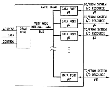
As previously noted, the basic structure provided by the AMPIC DRAM device of
said
copending application is illustrated in Fig. I, providing a very high
bandwidth connection between
system I/O resources # I ..#n via corresponding data ports through the DRAM
memory array located
within the AMPIC DRAM device. The flexibility of such an AMPIC DRAM device is
further enhanced,
as also earlier noted, by the ability to 'stack' multiple AMPIC DRAM devices,
as illustrated in the
example of Fig. 2. 1n Fig. 2, a system consisting of four AMPIC DRAM devices
is illustrated, AMPIC
#0 - #3; the actual number of AMPIC DRAM devices in a system being limited
only by the technology
constraints. When such stacks or arrays of AMPIC DRAM devices are created, the
total DRAM array
size available to the system UO resources is equal to the DRAM array size of
each AMPIC DRAM
device multiplied by the number of devices in the stack. For example, if each
AMPIC DRAM illustrated
in Fig. 2 is assumed to contain 64M bits of DRAM, then the AMPIC DRAM stack #0
- #3 illustrated will
provide a 256M bit DRAM array to the system I/O resources # 1 - #4.
While such an architecture does provide a very large amount of bandwidth for
each system UO
resource to access the DRAM, the system does not enable one system I/O
resource to send data to
another system UO resource, as earlier pointed out. For example, if system UO
resource r~r has a 32K bit
message it needs to send to system UO resource n, then once system I/O
resource rrr has written the
message into the AMPIC DRAM array #0 - #3, then a new mechanism must be
provided as by the
present invention to inform system UO resource ~r of both the existence of a
message, and of the message
location within the AMPIC DRAM array. Unce system 1/O resource rr has been
informed of the message
existence and of the message location in the AMPIC DRAM array, furthermore, an
additional novel
mechanism must be provided, again in accordance with the present invention, to
allow system Il0
resource n to extract the message from the AMPIC DRAM array. It is important
to note, as earlier stated,
that while the message data is distributed across the entire AMPIC DRAM array,
with each element of
CA 02297836 2000-O1-20
WO 99105604 PCTIIB98/01121
the array holding only a portion of the data, the complete signaling
information must be sent to each
individual element of the AI~1PIC DRAM array.
Assuming the existence of a novel mechanism of the type alluded to above and
later
described as provided by the present invention, by which system Il0 resources
may send messages to
each other through the AMPIC DRAM array, in the illustrative exarnple of
system 1/0 resource rn
transferring a 32K bit message to system I/O resource n, the I Kbyte internal
data bus would allow the
message to be transferred between the two system UO resources in only 2 AMPIC
DRAM transfer
cycles. For the purposes of illustration, if an AMPIC DRAM transfer cycle is
assumed to be 50 nano-
seconds (nS) in duration, the total bandwidth available within the AMPIC DRAM
is seen to be 32K bits
per SOnS or 655 gigabits per second. This very wide bus, however, is less well
suited to transferring
small messages between system I/O resources. An application where small
messages will need to be
transferred between system I/O resources, for example, is in ATM networking.
In ATM, data is
transferred in units of only 424 bits. If system I/O resources m and n are
both ATM network devices,
then system Il0 resource m may have a 424 bit message to send to system I/O
resource n. In this case,
the 32K bit wide internal bus will be used to complete the transfer in only 2
AMPIC DRAM transfer
cycles, but a very large amount of the internal bus is wasted in this
transfer. Even though the message
occupies only 424 bits of the 32K bit wide bus, all other system I/O resources
will be unable to use the
data bus during the time that system I/O resources m and n are completing
their transfer. If an AMPIC
DRAM transfer cycle is again assumed to be SOnS for the purposes of this
example, the total bandwidth
used in this example is only 424 bits per SOnS or about 8.5 gigabits per
second. Note that only about
1.3~1c of the bandwidth available within the AMPIC DRAM is actually utilized
in this example.
The present invention discloses an approach whereby the very wide internal
data bus will be
more efficiently utilized in such situations, further enhancing the usefulness
of the AMPIC DRAM
architecture by making it equally well suited for small and large units of
data transfer.
CA 02297836 2000-O1-20
WO 99/05604 PCT/IB98101121
It is now in order to discuss architectures by which the present invention
achieves these
improvements. Specifically, when system IIO resource nr has a message to be
written into the AMPIC
DRAM, the system IIO resource must be able to inform ail of the AMPIC DRAMS in
the system as to the
DRAM address at which to place the message. The present invention provides the
architecture and
mechanism disclosed in Fig. 3 for achieving this result. In the system
illustrated in Fig. 3, the four
AMPIC DRAMs of Fig. 2 are shown as CHIP 0 - 3, each with a I bit wide serial
interface to the system
I/O resource. In the example of Fig. 2, as disclosed in said co-pending
application, on the first cycle of
the data transfer, CHIP 0 gets data bit 0, CHIP I gets data bit 8, CHIP 2 gets
data bit 16, and CHIP 3 gets
data bit 24. On the next clock cycle, all the data bits are incremented. This
process continues until the
entire message has been sent to the AMPIC DRAM.
In accordance with the present invention, as illustrated in Fig. 3, concurrent
with this data ,
transfer, the system I/O resource will also be required to transfer the
address at which to place the data in
the DRAM. The width of the address register in the system I/O resource will be
determined by the size
of the DRAM array in the ANIP1C DRAM and the number of AMPIC DRAM devices in
the system.
From the before-mentioned example, a system with four AMP1C DRAM devices, each
of which
contains 64M/ bits of DRAIvI, will provide a 256M bit AMPIC DRAM array,
requiring 25 address bits.
Due to the large number of address bits required by large memory arrays,
however, it may be necessary
to define the address bus between the system I/O resource and the AMPIC DRAM
to be narrower than
the total address size, and use several transfers to transmit the complete
address into the AMPIC DRAM.
For example, if the address bus were defined as 4 bits wide, then 7 cycles
could be used to transfer the
complete 25 bit address into the AMPIC DRAM. This address transfer would take
place concurrently
with the data transfer from the system IIO resource, as illustrated in Fig. 3.
On the first cycle of the
transfer, bits 0 through 3 of the "Address" are transferred. On the second
cycle, bits 4 through 7 of the
Address are transferred, and so on until the entire address has been
transferred to all the AMPIC
DRAMS. It is important to note that, unlike in the data transfer, where each
AMPIC DRAM in the
CA 02297836 2000-O1-20
WO 99/05604 PCT/IB98/01121
system receives a different portion of the data, each AMPIC DRAM in the system
of Fig. 3 will receive
an identical copy of the complete DRAM address, thus causing each AMPIC DRAM
to write the
message transmitted by the system I/O resource into the same location in the
internal DRAM array.
In order for the message to reach its destination system I/O resource, a
similar addressing process
must occur at the destination side, as shown in Fig. 3a. Once system I/O
resource m has written the
message into the AMPIC DRAM array, the address at which the message was
written and the total size of
the message must be forwarded to the destination system I/O resource. The
destination system 1l0
resource, upon receiving the address of the message, will drive that address
into each of the AMPIC
DRAM devices. Each AMPIC DRAM device will proceed to read its portion of the
message data out of
its DRAM array from the given address and forward the message on to the
destination system I/O
resource. In the preferred embodiment of the invention, the size of the
message is also stored in the
DRAM array when the message is written into the DRAM array. As the AMPIC DRAM
device receives
the message, it counts the number of bits in the message; as illustrated in
Fig. 3, a Data Valid signal is
provided on ail the AMPIC DRAM data receive ports. The source system I/O
resource holds Data Valid
asserted for as long as the message data is being transmitted to the AMPIC
DRAM, and the AMPIC
DRAM uses this assertion of the Data Valid signal to determine the length of
the message. When the
data is written to the DRAM array, this bit count is stored along with the
message itself. When the
message is read out of the DRAM array, the corresponding bit count is read out
aion~ with the data. The
AMPIC DRAM then uses this bit count to determine the length of the message to
be transmitted. The
AMPIC DRAM indicates the size of the message to the destination system I/O
resource by asserting the
Data Valid signal for as long as is indicated by the message bit count.
The presence of each message DRAM address within each AMPIC DRAM device also
provides
an efficierrt solution for the case of one system I/O resource having a single
message which must be sent
to several other system I/0 resources, which is illustrated in Fig. 4. A
message of this type is defined as a
multicast message. in the case of a multicast message, the source system I/O
resource writes the message
CA 02297836 2000-O1-20
WO 99/05604 PCT/IB98I01121
into the AMPIC DRAM in the same way a standard, or unicast, message is
written. The address of this
multicast message within the DRAM array is then forwarded to all of the system
I/O resources which are
required to receive the message. Each of the destination system UO resources #
I - #m then proceeds to
drive the address of the multicast message into the AMPIC DRAM device. Given
that the AMPIC
DRAM device is provided with the address compare logic, illustrated in Fig. 4,
which can compare
DRAM addresses received from different system I/O resources, the multicast
control portion of the
AMPIC DRAM then recognizes that the same DRAM address was received from each
of the multicast
message system UO resources, and only needs to execute a single DRAM read
cycle. The DRAM data
from that read cycle is then forwarded to all of the destination system UO
resources #I - #m at the same
time by the multicast control logic illustrated in Fig. 4, thus eliminating
the requirement of several
DRAM reads for multicast messages.
In the preferred embodiment of the invention, the total number of address bits
required to specify
the DRAM location at which to write the message is further reduced by
logically partitioning the DRAM
into many equally sized sections. For example, in the case of a 256M bit AMPIC
DRAM array spread
across four AMPIC DRANf devices, the array may be divided, for example, into
2048 bit sections. In
this case, the DRAM array would now consist of 128K sections; each AMPIC DRAM
device would
store S l2 bits of each of the 128K sections. As a result, only 17 address
bits would be required
completely to specify the address to the AMPIC DRAM. Going back to the example
of a 4 bit wide
address bus, only 5 cycles would now be required to transfer the address from
the system IIO resource
into all of the AMPIC DRAM devices. In so partitioning the memory, it may be
desirable to keep the
size of the sections small, so as to minimize wasted memory space. In the
above example of 2048 bit
sections, if, for example, system I/O resource m has a 5l2 bit message to
write into the AMPIC DRAM,
then the message will only partially fill a DRAM section, resulting in wasted
memory space.
White maintaining small section sizes, however, the invention also provides a
mechanism to
handle cases 4vhere system Il0 resource m may have a message to be written
into the AMPIC DRAM
9
CA 02297836 2000-O1-20
WO 99105604 PCTIIB98101121
which is larger than a section. The solution to this problem in the preferred
embodiment of the invention
is illustrated in Fig. 5. Each DRAM section #A - #C reserves some number of
bits to contain what is
referred to as a Link Address. When system Il0 resource m has a message to
write into the AMPIC
DRAM which is larger than the currently defined section size, the system IIO
resource will first need to
divide the message into several pieces, the size of each being less than or
equal to the currently defined
section size. The first piece of the message will be placed into the first
DRAM section, and the Link
Address of that section wilt be set to point to the next DRAM section, into
which the second piece of the
message will be placed, and so on, until the entire message has been written
into the AMPIC DRAM
array. The result for an example in which a message occupies 3 DRAM sections
is illustrated in Fig. 5.
For purposes of illustration, a message size of 5120 bits will be assumed, and
the section size will be
assumed to be 2048 bits, as explained above. In this case, bits I-2048 of the
message will reside in
DRAM Section #A, bits 2049-4096 will reside in DRAM Section #B, and bits 4097-
5120 will reside in
DRAM Section #C, resulting in a partially filled DRAM Section, as illustrated
in Fig. 5. Because the
Link Address is stored in the AMPIC DRAM array along with the message data,
the AMPIC DRAM
reassembles the complete message when sending the message to the destination
system 1l0 resource.
When a section is read out of the AMPIC DRAM array, logic in the AMPIC DRAM
examines the section
Link Address portion to determine if this DRAM section is one part of a larger
message. If the Link
Address points to another section of the DRAM, then the AMPIC DRAM reads that
section out of the
DRAM array for forwarding to the destination port. This process continues
until the AMPIC DRAM
finds a DRAM section the Link Address of which does not point to another
section, at which point the
entire message has been reassembled. This message reassembly occurs without
any intervention on the
part of the destination system I/O resource; it is handled entirely by logic
within the AMPIC DRAM.
In an alternate embodiment of the invention, the section size is not fixed
within the AMPIC, but
is instead programmable to a range of different values as illustrated in Fig.
6. For example, in a system
where primarily small messages are passed between system I/O resources, the
section size may be set to,
rB
CA 02297836 2000-O1-20
WO 99!05604 PCTIIB9$101121
say, 256 bits. In a system where primarily large messages are passed between
system I/O resources, the
section size may be set to, for example, 2048 bits. A range of such sizes
would be provided by the
AMPIC DRAM device, in order to maximize the use of the DRAM array and minimize
wasted memory
space caused by messages which are smaller than the section size. In Fig. 6,
an example of three
different section sizes, A, B, and C, and the resulting structure of the DRAM
array are presented. In an
additional alternate embodiment, wasted DRAM space may be totally eliminated
by not dividing the
DRAM array into sections at all, as illustrated in Fig. 7. In this embodiment,
messages are always placed
into the DRAM array back to back, regardless of their size. While increasing
the number of address bits
required to keep track of DRAM addresses, this embodiment has the advantage of
using the memory
most efficiently, Fig. 7 illustrating how different-sized messages may be
distributed throughout the
DRAM array.
In the preferred form of the invention, all the passing of addresses between
source
system I/O resources and destination I/O resources takes place in logic
external to the AMPIC DRAM.
In an alternate embodiment, this function is handled by the AMPIC DRAM itself,
as illustrated in Fig. 8.
Here, all addressing and passing of addresses from source system I/O resource
to destination system I/O
resources takes place inside the AMPIC DRAM itself. In this embodiment, the
system Il0 resources
need no knowledge of the DRAM address at which messages are located within the
AMPIC DRAM
array. For example, if the source system IIO resource had a message to send to
the destination system
I/O resource, then the source system I/O resource would send the message data
into the AMPIC DRAMS,
without also needing to drive in an address. It should be noted that Fig. 8
illustrates only a single AMPIC
DRAM device; the discussion, however, being equally applicable to a system
consisting of multiple
AMPIC DRAMS, as previously discussed. Upon receiving the message data, the
AMPIC DRAM
chooses a free address in its DRAM array from the free address list and writes
the message to that
location. That address is then forwarded to the AMPIC DRAM port to which the
destination system I/O
resource is connected. The AMPIC DRAM then informs the destination system IIO
resource of the
CA 02297836 2000-O1-20
WO 99/05604 PCTlIB98/01121
existence of a message for it within the AMPIC DRAM using the Message Ready
signal illustrated in
Fig. 8. At some point later, the destination system I/O resource signals that
it is ready to accept the
message via the Il0 Resource Ready signal of Fig. 8, at which point each AMPIC
DRAM device
retrieves its portion of the message data from its DRAM array and forwards the
data on to the destination
system I/O resource. In this way, the system UO resources are made completely
independent of the
internal structure of the AMPIC DRAM devices; the AMPIC DRAM array functions
as a store and
forward a: X r: cross-connect array. In this embodiment, in addition to
keeping track of the locations of
messages in the DRAM array, the AMPIC DRAM must also keep track of the amount
of free space
remaining in the DRAM array. As the DRAM array begins to fill up, the AMPIC
DRAM must be able to
signal the system I/O resources not to send any messages for some period of
time, anti! the DRAM array
has started to empty out. The Free Address List, as illustrated in Fig. 8, is
used for this purpose.
It is now in order to describe a preferred mechanism by which data is
transferred within
the AMPIC DRAM devices as illustrated in Fig. 9. The DRAM array of an AMPIC
DRAM device is
shown physically divided or partitioned into several independently controlled
banks; the actual number
of DRAM banks implemented (DRAM Banks I - m) wilt depend only on the
technology used to
implement the AMPIC DRAM. In order to simplify the discussion, a system
consisting of only a single
AMPIC DRAM device will accordingly be discussed here, the discussion being
equally applicable to
systems consisting of multiple AMPIC DRAM devices. In the latter case, the
DRAM array in each
AMPIC DRAM device will be partitioned identically.
Preferably, the number of DRAM banks will be greater than or equal to the
number of system Il0
resources which can be connected to the AMPIC DRAM. The very wide internal
data bus is shown in
Fig. 9 evenly divided between each of the DRAM banks. For example, in an AMP1C
DRAM
implementation with 64 DRAM banks and a 32K bit wide data bus, the data bus
for each DRAM bank
would be 512 bits wide; the sixty-four 512 bit wide buses would combine to
form the complete 32K bit
wide data bus. As disclosed in said copending application and in Fig. I, each
system I/O resource is
t2
CA 02297836 2000-O1-20
WO 99/05604 PCTIIB98/01121
connected to a data port within the AMPIC DRAM, which in turn connects to the
internal very wide data
bus. In the embodiment illustrated in Fig. 9, each of these data ports is
divided into a number of slots (0-
m); the number of slots in each data port being equal to the number of DRAM
banks. In the before-
mentioned example, each data port will be 32K bits wide, and will be divided
into 64 sections of 512 bits
each. Each slot corresponds to a single bank of the DRANI array. As data
arrives from the system I!O
resource, the data is streamed into the appropriate slot of that system IIO
resource data port; the
appropriate slot being determined by the DRAM address to which the data is to
be written, which will in
turn determine into which DRAM bank the data is written. It should be recalled
that in the preferred
embodiment of the invention, this address is provided by the system UO
resource concurrent with the
message data. If the incoming message is, for example, 32K bits wide, then the
entire message may be
streamed into all 64 slots of the data port, and then written into the DRAM
array in a single AMPIC
DRAM write cycle. If an illustrative value of SOnS is once again assumed for
the duration of an AMPIC
DRAM transfer cycle, the resultant internal AMPIC DRAM bandwidth is seen to be
32K bits per SOnS or
655 gigabits per second.
Alternately, returning to the previously mentioned example of ATM networking,
if the incoming
message is very short, for example, 424 bits, then only one slot of the system
I/O resource data port need
be used. In this case, if several other system I/O resources have filled
different slots of their data ports
with similarly sized messages, all of those messages may be transferred to the
DRAM at the same time,
allowing for more efficient utilization of the very wide data bus.
Alternately, a single system I/O
resource may be allowed to accumulate multiple short messages, filling several
slots of its data port
before writing the message data into the DRAM array. It should be noted that a
single system UO
resource may only accumulate several short messages in its data port if each
of the messages is destined
for a different DRAM bank, as indicated by the message addresses. In either
case, in the current example
of 64 DRAM banks, up to 64 messages may be transferred within the AMPiC DRAM
simultaneously,
whether from the same system 1/0 resource, or from many different system UO
resources. Using the
l3
CA 02297836 2000-O1-20
WO 99/05604 PCTIIB98101121
illustrative figure of SOnS for the duration of an AMPIC DRAM transfer cycle,
the utilized bandwidth for
ATM networking is therefore calculated to be (64*424) bits per SOnS or 542
gigabits per second, or
almost 83~1c of the total available bandwidth. This total bandwidth
utilization will increase as the number
of DRAM banks provided in the AMPIC DRAM device is increased. The DRAM and
buffering
stmcture herein disclosed, therefore, provides a balance between support of
small numbers of very wide
data transfers, and larger numbers of small data transfers, by allowing
several small data transfers from
different system Il0 resources to occur simultaneously.
The previously described embodiment of this invention, however, has a
timitation when a system
I/O resource sends two consecutive messages into the AMPiC DRAM both of which
are destined for the
same DRAM bank. In this special case, since both messages must use the same
slot of the data port, the
second message must wait until after the first message has been written into
the DRAM array before
being written into the data port. An alternate embodiment of the invention for
alleviating this problem is
illustrated in Fig. 10. In this embodiment, an mXn crossbar switch is placed
between each system I/O
resource data port (1-n) and the DRAM array (banks 1-m). In this case, the
DRAM array consists of m
banks and the buffer consists of s slots. The crossbar switch enables any
section of the buffer to be
driven to any one of the DRAM banks, therefore making the buffer independent
of the DRAM address
used; rather than controlling into which buffer section the data mutt be
written, the DRAM address will
control the functioning of the switch. In this example, if system IIO resource
1 has written 424 bits into
data port slot 0 destined for DRAM bank I and system I/O resource n has also
written 424 bits into slot 1
of its data port destined for DRAM bank m, then both messages may be written
into the DRAM
simultaneously. Logic in the AMPIC DRAM will need to control each port switch
appropriately to
switch the correct data port slots} to the correct DRAM banks) for each
transfer. It is important to note
that this switch will also need to operate bidirectionally; that is, for reads
of the DRAM where data is to
be transmitted from the AMPIC DRAM to a system I/O resource, the switch must
be able to move data
from the correct DRAM banks into the proper data port slots. While not
altering the total bandwidth
14
CA 02297836 2000-O1-20
WO 99/05604 PCT/IB98/01121
utilization provided by the preferred embodiment of this invention, by
providing address-independence in
the use of buffer sections, the crossbar switch in this alternate embodiment
allows for much more flexible
use of the entire data port. In the before-mentioned example of a system I/O
resource driving two
consecutive messages into the AMPIC DRAM both destined for the same DRAM bank
for example, the
second message is now written into the next available slot of the data port,
regardless of its eventual
destination DRAM bank. The mXn crossbar switch is used to forward the message
to the appropriate
DRAM bank when the time comes to write the message into the DRAM.
Further modifications wilt also occur to those skilled in this art, and such
are considered to fall
within the spirit and scope of the invention as defined in the appended
claims.