Note: Descriptions are shown in the official language in which they were submitted.
CA 02298187 2000-02-07
N. M. Denlcin Case 7-1-1 1
A REDUNDANT REGULATED POWER SUPPLY SYSTEM WITH
MONITORING OF THE BACKUP POWER SUPPLY
Field Of The Invention:
The invention relates to redundant power supply systems and more particularly
relates to monitoring concurrently the active and backup power supplies.
Background Of The Invention:
Critical circuits within a complex electronic system require a highly reliable
source of regulated power. Such systems typically employ several power
supplies, active
and backup power supplies, to provide the required reliability. A conventional
method of
combining redundant power supplies uses diodes to "Or" the outputs of the
power
supplies. To regulate the level of the voltage that is being supplied to the
drain (load),
the voltage at the drain is sensed and fed back to each of the redundant power
supplies
As will be explained below in detail, each such power supply compares the
value of the
sensed signal with the value of a respective preset signal and changes its
output as a
function of the difference between the sensed and preset values. Such
regulation may
have the effect of causing the output voltage level of one of the power
supplies ( typically
the backup power supply) to decrease significantly, while the other power
supply mrtputs
an acceptable voltage level. Apparatus that monitors the backup power supply
would
thus be unable to determine if that power supply is operating properly, and,
more lik~lv.
would incorrectly conclude that the backup supply has failed.
Summary Of The Invention:
We have recognized that the foregoing problem may be dealt with, in am«r.i,mce
with an aspect of the invention, by using as the sense signal a feedback
signal that ~~
derived as a function of both the voltage signal outputted by a power supply
anti the
~5 voltage signal (sensed signal) delivered to the load. Accordingly, then,
the red=ul,m;~n ~~t
the outputted voltage signal is based un both the outputted voltage signal and
:en.«i
voltage signal. More specifically. m accordance with various aspects of the
inventran ,r
. . CA 02298187 2000-02-07
N. M. Denkin Case 7-1-1 2
. feedback signal that is supplied to a power supply as the sensed signal is
derived using a
voltage divider network across the output of the power supply and a common
connection at which the sensed voltage is derived. A power supply then
regulates its
output voltage as a function of the level of the feedback signal and the level
of the preset
signal.
These and other aspects of the invention will become more apparent from the
following detailed description read in conjunction with the accompanying
drawings.
Brief Description Of The Drawing
In the drawing:
FIG. 1 is broad block diagram of a conventional regulated power supply;
FIG. 2 is broad block diagram of a redundant power supply system regulated in
the manner shown in FIG. 1;
FIG. 3 is broad block diagram of redundant power supply system regulated in
accordance with the principles of the invention.
I 5 Detailed Description:
The prior art system illustrated in FIG. 1 includes power supply 10 and load
~o
represented by resistor RL. Power supply 10 outputs to path 1 1 a voltage
level derived
as a function of an externally supplied preset voltage level, V,<<, which may
be e;t,rhl~.hed
via one of a number of dif~'erent conventional ways, e.g., programming, zener
di~~~ir
precision bridge, etc. Path l l may include distributed resistance
(represented in the I~ I(
by resistor 20 also designated Rd) which decrease the level of the voltage
that supply I ~ ~
provides to load 30. The actual level of the voltage .that is supplied to load
30 is aen.ed
in a conventional way and fed via path I '_' to one input of instrumentation
amplifier -i~ ~
whose gain is set by the value of resistor Rg. Amplifier 40 compares the
sensed w~lta~_e
level with the preset voltage level, t',,,, that is supplied to another input
of ampl~tier -i~
Amplifier 40 then outputs to voltage s~enerator ~0 an error signal that is
indicativ a ut the
CA 02298187 2000-02-07
N. M. Denkin Case 7-1-1 3
difference between the level of the sensed voltage and preset voltage. Voltage
generator
50, in a conventional manner, changes the level of the voltage signal that it
is supplying
to path 11 with respect to ground. For example, if the sensed voltage is lower
(higher)
than the preset voltage, then generator 50 increases (decreases) the level of
the voltage
signal that it is outputting to path 1 1. An equilibrium is reached when the
level of the
sensed voltage equals the level of the preset voltage, Vse~.
This voltage regulation scheme may be applied in a conventional manner to a
system having redundant power supplies, as shown in FIG. 2, in which each of
the power
supplies 100 and 200 are similar to power supply 10 of FIG. 1. Also, voltage
supply
paths 211 and 212 extending to load 130 (represented by RL2) may similarly
include
some distributed resistance respectively represented by resistors Rd21 and
Rd22 Diodes
D21 and D22 provide an Or function as well as isolating power supplies 100 and
200
from one another. The level of voltage supplied to load 130 via path 121 with
respect to
ground is sensed by sense paths 213 and 2l4 respectively connected to supplies
100 and
200 in the manner shown in FIG. 1. As discussed above, power supply 100
adjusts the
level of the voltage that it is outputting across path 211 and ground as a
function of the
difference between the levels of the sensed voltage level supplied via path 21
(sen,e~ I 1
and preset voltage Vsetzr. Power supply 200 operates similarly with respect to
the
sensed voltage level supplied via path 214 (sense22) and preset voltage
Vset~,.
We have recognized that a problem arises when the values of the preset
volta~,e,,
Vset2r and Vset22 have approximately the same nominal value, but do not
actually equal
one another. Specifically, the power supply connected to the higher preset
volta~,e level
continues to increase the level of the voltage signal that it is supplying to
load 1 si) unUl
the level of the voltage at path I'? 1 equals the higher preset voltage level.
The power
supply that is connected to the lower preset voltage level, on the other hand,
cononues
to decrease the level of the voltage signal that it is supplying to load 130
as a wry «t
attempting to match its preset voltage level with the voltage level supplied
via :en.r h.rth
214. For example, assume that preset volta~,e Vset~, equals +5.3 volts and
preset wlt,a_~
VsetzZ equals +5.2 volts. Although the preset voltage levels nominally equal
one anther
. . CA 02298187 2000-02-07
N. M. Denkin Case 7-1-1 4
and are within a specified limit, power supply 100 will, nevertheless,
increase its output
to a point where the voltage supplied to load 130 equals +5.3. Power supply
200
"seeing" that the sensed voltage of +5.3 volts is greater than its preset
voltage of +5.~
volts decreases the level of its output voltage to drive the voltage that is
being supplied
to load 130 toward a value of+5.2 volts. Each time power supply 200 decreases
the
level of its output voltage. the difference between the sensed voltage level
and Vset~,
increases. Disadvantageously, power supply 200 continues to operate in this
manner until
the level of the voltage signal that it is outputting effectively reaches
zero. At that point,
monitor 400 may conclude that power supply 200 is not operating properly and
may
output an alarm message indicating that the power supply failed. A
craftsperson
responding to the message may then replace the supposedly failed power supply
200
We have further recognized that the foregoing problem may be dealt with by
forcing both power supplies to operate as expected. We do this, in accordance
with an
aspect of the invention, by "tailoring" the sensed voltage level that is
supplied to a poorer
1 S supply to the preset voltage level that is connected to that power supply.
Such tailoring
may be achieved, in accordance with another aspect of the invention, by
sensing the
voltage level at the load and at the output of a power supply using, for
example, a
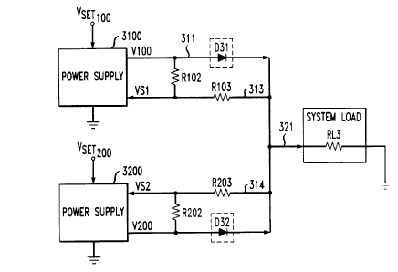
voltage divider across a respective "Oring" diode as is shown in FIG. 3. In
this wav, a
voltage level with respect to ground will appear at the junction of resistors
R 102 and
8103 (R202 and 8203) between the voltage level at 31 1 (312) and the voltage
level at
321. In effect, the difference between the voltage level at 31 I (312) and
voltage level at
321 will be the voltage drop across diode D31 (D32). In an illustrative
embodiment ut
the invention, diodes D31 and D32 are Shottky diodes having a voltage drop in
the ran';e
of, for example, 0.2 volts. Thus, the sensed voltage is a value that is
weighted in
accordance with the values of the resistors forming the voltage divider,
which, in
accordance with an illustrative embodiment of the invention, equal one another
and each
may have a value of, e.g., 100,000 ohms.
With reference to FIG 3, the sensed voltage, Vsl, supplied to supply 31OO may
be expressed as follows:
CA 02298187 2000-02-07
N. M. Denkin Case 7-1-1 5
Vsl = (R103*V100 + 8102*Vout) (1)
R 102 + R 103
where V 100 is the output voltage at power supply 3100 and Vout is the voltage
level at
321. The sensed voltage supplied to power supply 3200 may be similarly
expressed as
follows:
Vs2 = (R203*V200 + 8202*Vout) (2)
8202 + 8203
where V200 is the output voltage at power supply 3200 and, as mentioned above,
'out
is the voltage level at 321.
Based on the foregoing, power supplies 3 l00 and 3200 may now independently
adjust their respective output voltages, V 100 and V200, such that the sensed
voltages
supplied to those power may be adjusted to equal the respective preset voltage
level, as
will be shown below. Thus, assume that the level of Vset,oo is greater than
the level of
Vset2~~. For that case we may express Vset3, as follows:
I S Vset,~~ _ (R103*V 100 + 8102*Vout) (3)
8102 + 8103
Solving for Vout yields the following expression:
Vout = R103LVset"", - v100) + Vset,~~ (4)
8102
In general, Vout and V l00 dit~'er by an amount related to the voltage drop
through Oring diode D31, which may be, for example, a Shottky diode. As is
well
known, the voltage drop, S(I) across a Shottky diode is approximately 200 my
ff we
letting V 100 = 8(I) + Vout, then the equation for Vout may be re-written as
tolluw
Vout = Vset"~~~ - u~l~*R I03 (5)
R I O? - R 103
It is noted that V"~, will he somewhat less than the setpoint V,C~",". For thr
~,~.r
where 8102 = 8103, the difference should be approximately 100 my Increasing,
the
resistance of 8102 will minimize this dit~erence.
CA 02298187 2000-02-07
N. M. Denkin Case 7-1-1 6
The output voltage V200 in terms of V 100 may be determined starting with
following expression:
(8102 + 8103)*Vset,~o -8102*V 100 = (8202 + 8203;1 *Vset2~~ -8202*V200 (6)
8102 8202
If the values of all of the resistors are equal, then (6) may be expressed as
follows:
2*Vsetl~~, - V100 = 2*Vset2~o, - V200 (7)
If Vset,~", = Vsetzoo + 0, then V200 in (7) may be expressed as follows
V200 = V100 - 2*:~ (8)
Thus, as shown by equation (8), when the monitor of FIG. 2 observes the
outputs of power supplies 3100 and 3200 it will find that the voltage level
V200 will be
slightly less the voltage level V 100 -- differing by merely the twice the
difference
between the setpoints --, thereby confirming that power supply 3200 is
operating
properly, all in accordance with an aspect of the invention.
It will thus be appreciated that, although the invention illustrated herein i,
described in the context of a specific illustrative embodiment, those skilled
in the art will
be able to devise numerous alternative arrangement which, although, not
explicitly
shown or described herein, nevertheless, embody the principles of invention
and are
within its spirit and scope.