Note: Descriptions are shown in the official language in which they were submitted.
CA 02298310 2000-02-09
1
Title
Low-Voltage Transconductance Amplifier/Filters
Field of Invention
S The invention resides in the field of wireless communication devices and
systems where a wide variety of signals need to be handled. In particular it
relates
to transconductance cells for amplifying/filtering wireless signals, which
cells
have a high linearity over a wide range of signal levels and yet require a low
operational voltage.
Background of Invention
In typical applications, a wireless receiver must operate over a wide range
of signal levels as well as large interfering signals. The interfering signals
emanate from users in adjacent channels, as well as from transmission sources
1 S which may be relatively far removed in frequency but have a large
transmission
power. When two interfering signals at frequencies fl and fZ (where fl and fZ
are
close to the desired signal frequency) are present, they will produce -due to
amplifier nonlinearity- intermodulation products at frequencies 2f2 fl and 2fl
fl.
These can fall at frequencies close to the desired signal frequency. The
resulting
interference causes measurable degradation of the bit error rate (BER) in
digital
communication systems.
The ability of circuits to handle large signals can be characterized by the
third-order intercept point (IP3) which is a measure of circuit linearity. In
most
receivers, signal filtering circuits and variable gain control circuits are
essential
parts of signal processing to decode the transmitted information. These
circuits
often use transconductance amplifiers/filters as building blocks as they
satisfy the
requirements well. The transconductance amplifiers/filters are in the
configuration of differential amplifiers and are also called simply
differential
amplifiers.
Following articles describe in detail requirements of wireless
communication receivers and suggest some design principles of transconductance
amplifier/filters.
[1] Fenk J. and Sehrig P.: "Low-noise, low-voltage, low-power IF gain
controlled amplifiers for wireless communications," in Analog Circuit Design,
Huijsing J.H. et al. (eds), 1996 Kluwer Academic Publishers, pp. 27-44.
, CA 02298310 2000-02-09
2
[2] Crols J., Steyart M.: "Low-IF Topologies for High-Performance
Analog Front Ends of Fully Integrated Receivers," "IEEE Transactions on
circuits
and systems-11.~ Analog and digital signal processing," Vol. 45, No. 3, Maxch
1998, pp. 269-282.
There is a further requirement however of these signal filtering and
variable gain control circuits and that is that they must be powered at a very
low
voltage.
An article below describes cascaded current mirror circuits which permit
low voltage operation of transconductance amplifiers.
[3] Crawley P. J., Roberts G. W.: "Designing Operational
Transconductance Amplifiers For Low Voltage Operation" "IEEE International
Symposium on Circuits and systems" Chicago, Illinois, May 1993, pp. 1455-1458.
Following U.S. Patents describe a variety of transconductance amplifiers:
U.S. Patent No. 5,444,414 Aug. 22, 1995 Delano, U.S. Patent No. 5,451,901 Sep.
19, 1995 Welland and U.S. Patent No. 5,844,442 Dec. 1, 1998 Brehmer.
In spite of the prior art mentioned above, there are pressing needs to have a
transconductance amplifier/filter that can operate at a low supply voltage and
yet
exhibit a high linearity. Some embodiments of the invention include a common
mode feedback circuit used to bias the transconductance amplifier and/or a
variable gain circuit to permit operation at a different gain settings.
In yet another embodiment, a complex filter cell includes four Gm
transconductance cells to realize a complex pole filter. More poles can be
realized
using cascaded complex Gm cells. A wireless communications receiver including
such filters is also described.
The specification will describe the invention and its advantages in full in
connection with circuits which use bipolar transistors. It should, however, be
noted that any active devices including e.g., MOS etc., can be used to
implement
the present invention to realize the advantages.
Summary of the invention
According to one aspect, the invention is directed to a transconductance
cell which operates at a low supply voltage and has a high linearity. The cell
comprises a transconductance core for differential inputs and differential
outputs,
current sources for providing operational currents for the transconductance
core
and current mirror circuits connected to the transconductance core for
generating a
CA 02298310 2000-02-09
pair of mirrored feedback currents to be fed back to the current sources.
According to a further aspect, a complex filter for a differential signal
comprises at least four transconductance cells. Each transconductance cell has
a
transconductance core for differential inputs and differential outputs and
current
sources for providing operational currents for the transconductance core,
current
mirror circuits for generating a pair of mirrored feedback currents to be fed
back
to the current sources; a bias circuit for setting an operational point of the
transconductance core and a common mode feedback circuit for generating a bias
signal to be applied to the bias circuit. The first transconductance cell has
the
differential signal as first differential inputs to generate first
differential outputs
and the second transconductance cell has a phase-shifted differential signal
which
is 90 degrees out of phase with the differential signal as second differential
inputs
to generate second differential outputs. The third transconductance cell is
connected in parallel with the first transconductance cell and generates
jointly
therewith the first differential outputs in response to the second
differential
outputs. Finally the fourth transconductance cell is connected in parallel
with the
second transconductance cell and generates jointly therewith the second
differential outputs in response to the first differential outputs.
Brief Description of Drawings
Figure 1 is a schematic diagram of a basic transconductance cell.
Figure 2 is a schematic diagram of a feedback transconductance cell.
Figure 3 is a schematic diagram of a variable gain transconductance cell.
Figure 4 is a schematic diagram showing a practical transconductance cell
implementation in accordance with one embodiment of the present invention.
Figure 5 is a schematic diagram of a common mode feedback circuit in
accordance with one embodiment of the invention.
Figure 6 is a block diagram of a Gm cell.
Figure 7 is a schematic diagram showing a variable-gain Gm cell.
Figure 8 is a graph showing the frequency response of a real band pass
filter.
Figure 9 is a graph showing the frequency response of a real low pass
filter.
Figure 10 is a graph showing the frequency response of a complex band
pass filter.
CA 02298310 2000-02-09
4
Figure 11 is a block diagram showing a single complex pole filter.
Figure 12 is a block diagram of a complex 7-pole filter in a cascaded
structure.
Figure 13 is the AC response of complex 7-pole filter.
Figure 14 is a block diagram showing a communication system in
accordance with an embodiment of the present invention.
Detailed Description of Preferred Embodiments of Invention
Figure 1 presents a transconductance cell known in the art. The cell
includes a transconductance core consists of two transistors Q1, Q2, that are
coupled to differential inputs In+ and In-. A degeneration resistor Re couples
the
emitters of transistors Q 1 and Q2 to the current sources Io 1 and Io2. This
degeneration resistor improves the third order intercept point IP3 of the
cell. In
the field of wireless communication devices, the incoming signals can be radio
frequency (RF) or intermediate frequency (IF) signals. The incoming signal is
present at the input ports, In+ and In- as a differential (balanced) voltage
signal.
The differential signal consists of a non-inverted and an inverted signal. The
differential voltage signal is converted and amplified using the transistors Q
1 and
Q2 into two differential currents Ic 1 and Ic2. The device that converts a
voltage
signal into a current signal and amplifies this signal before presenting an
amplified
voltage signal is called transconductance cell. The resistors Rc 1 and Rc2 are
used
for converting current information into voltage information and to present the
information at the output ports Out- and Out+ as differential output voltage
signal
which consists of a non-inverted and inverted output signal.
Figure 2 shows an improved transconductance cell known in the art. The
transconductance cell includes transistors Q 1 and Q2 and feedback transistors
Q7
and Q8. A degeneration resistor Re couples the emitters of transistors Q1 and
Q2
and it improves linearity as in the case of Figure 1. These emitters are also
coupled to the collectors of transistors Q3 and Q4 which act as current
sources for
the input differential transistor pair Q1 and Q2. The incoming voltage signal
present at input ports Vin+ and Vin- is converted into two currents Icl and
Ic2 by
the differential transistor pair formed by Q1 and Q2, is amplified and is
converted
again into a differential voltage signal present between the bases of
transistors Q7
and Q8. This voltage is transferred through the base-emitter junctions of
transistors Q7 and Q8 into two voltages present at resistors Rbl and Rb2. The
CA 02298310 2000-02-09
voltage signals on resistors Rbl and Rb2 are applied to the bases of
transistors Q3
and Q4, which then feed these signals into the emitters of input transistors Q
1 and
Q2. Therefore, this circuit contains a feedback path; the input goes to Q 1
and Q2,
through Q7 and Q8 to Rb 1 and Rb2, through Q3 and Q4 and back to Q 1 and Q2.
5 This feedback of the amplified signal provides a further improvement to the
linearity of the transconductance cell. The output signal is developed through
transistors QS and Q6 and with Q3 and Q4, they sense the voltage at Rbl and
Rb2, and convert output current information into two output currents Ic5 and
Ic6.
The resistors Rc 1 and Rc2 convert output current information into output
voltage
information and present the information at the output port Out+ and Out- as a
differential output voltage signal consisting of a non-inverted and inverted
output
signal.
It should be noted that in the foregoing figures and any figures which may
follow, same or like designations indicate same or like components. Therefore,
for example, transistors Q 1 and Q2 in both Figures 1 and 2 are components
which
perform similar functions.
Figure 3 illustrates a dual-gain emitter-coupled differential variable gain
amplifier. In this circuit, the input transistor pair Q 1 and Q2 with
degeneration
resistor Rel, and also the transistor pair Q9 and Q10 with the resistor Re2
act as
two transconductance cores as presented in Figure 1. Each of two cores
converts
the input signal into a differential current. A gain select block GS controls
which
transconductance core is active by activating either the current sources Io 1
and Io2
for the transistor pair Q 1 and Q2 or the current sources Io3 and Io4 for the
transistor pair Q9 and Q10. The resistors Rcl and Rc2 convert the differential
current information Icl and Ic2 into a differential output voltage at the
output
ports Out+ and Out- as a differential output signal consisting of a non-
inverted
and inverted output signal.
In Figure 4 a schematic diagram showing a practical transconductance
implementation in accordance with one embodiment of the present invention is
presented. This implementation has at least two distinct advantages over the
prior
art presented in Figure 2. First, in Figure 2, the intermediate currents Ic 1
and Ic2
are converted to a voltage which modulates Rb 1 and Rb2; the new
transconductance cell in Figure 4 has no intermediate conversion from current
into
voltage. Keeping the signal entirely in the current domain provides better
linearity. Second, the structure in Figure 2 exhibits two series base-emitter
CA 02298310 2000-02-09
6
junctions at Q7 and Q3 (or two gate-source junctions if the circuit were built
using
MOS rather than bipolar transistors) between the positive power supply and
ground. Figure 4 does not exhibit this trait, permitting it to be used at a
lower
power supply voltage.
Referring to Figure 4, the input differential transistor pair Q 1 and Q2 with
degeneration resistor Re converts the input signal present at input ports Vin+
and
Vin- into a differential current represented by Icl and Ic2. Transistor pairs
M1-
M3 and M2-M4 produce feedback currents Ic 12 and Ic 11 mirrored from currents
Ic l and Ic2 respectively and feed them back into respective current mirror
transistors Q 12 and Q 11. Feedback currents Ic l2and Ic 11 are then mirrored
by
diode-connected current mirror transistor pair Q12 and Q1 l and fed into
transistor
pair Q4 and Q3 respectively. These latter two transistor pairs act like
current
sources for the input differential transistor pairs and also operate as
negative
feedback transistors for the transconductance currents Ic 1 and Ic2. The
negative
feedback without intermediate conversion from current to voltage improves the
linearity of the transconductance cell. In addition, as mentioned above, the
circuit
of Figure 4 includes no series base-emitter junctions which cause unnecessary
voltage drops. There is only one base-emitter junction at Q3 in Figure 4 and
as a
consequence, it can operate at a lower supply voltage. Figure 4 illustrates
also a
biasing circuit for the transconductance core which sets the point of
differential
operation. As seen in the Figure, the bias is provided by MS and M6 which
forces
four equal currents Ic 1, Ic2, Ic 11 and Ic 12. The bias transistors MS and M6
are
commonly biased from the port Vbias. Transistors Q5 and Q6 sense a
differential
current represented by Ic5 and Ic6 and then amplify this into a differential
current
represented by Ic5 and Ic6. The resistors Rcl and Rc2 convert the differential
current represented by Ic5 and Ic6 into a differential voltage at the output
ports
Out+ and Out-. The resistors Rc 1 and Rc2 and Re as well as the emitter area
ratios of QS/Q11 and Q6/Q12 are chosen to achieve the required gain value.
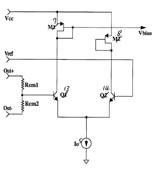
Figure 5 is a schematic diagram of a common mode feedback circuit. This
circuit provides the bias voltage for the transconductance cell shown in
Figure 4.
The differential pair represented by transistors Q 13 and Q 14 compares a
reference
voltage present at port Vref with a common mode voltage. The common mode
voltage is obtained from the two voltages present at ports Out+ and Out- that
are
connected through resistors Rcml and Rcm2. The middle point between the
resistors exhibits a common mode voltage that equals the average DC voltage of
CA 02298310 2000-02-09
7
the signals Out+ and Out-. Any difference between the common mode voltage
and the reference voltage is amplified by the differential pair and
transferred to the
loads represented by transistors M7 and M8. The bias voltage that results from
the process of comparison and amplification is presented at port Vbias.
Figure 6 shows a block diagram for a Gm cell 100 illustrating this
embodiment with a transconductance cell 102 and a common mode feedback
circuit 104. The output ports of the transconductance cell 102 are connected
to
the ports Out+ and Out- in the common mode feedback circuit, and the Vbias
port
in the common mode feedback circuit drives the Vbias port of the
transconductance cell 102.
Another preferred embodiment of the invention is illustrated in Figure 7.
In addition to input differential pair transistors Q 1 /Q2 and their current
source
transistors Q3/Q4 and degeneration resistor Rel, a second input differential
pair
Q9/Q10 is connected in parallel with Q1/Q2, and it has its own separate
current
source transistors Q 15/Q 16 and degeneration resistor Re2. Additionally, four
switches S 1, S2, S3, and S4 are placed in the emitters of respective current
source
transistors Q3, Q4, Q 15, and Q 16. These switches are controlled in pairs by
a
gain select block GS: typically, either S1 and S2 are closed while S3 and S4
are
open, or S3 and S4 are closed while S l and S2 are open. The current source
transistors connected to the closed switches are enabled, while those
connected to
the open switches are disabled. This, in turn, enables or disables the
corresponding input differential pair. By choosing different values for Re 1
and
Re2, and/or different emitter areas for current source transistors Q3/Q4
versus
Q15/Q16, two different gains can be realized. The gain select block can
therefore
open and close the switches to control the gain of the overall Gm cell.
Because
the gain of this cell can vary, the cell is called a variable-gain Gm cell.
In the above two embodiments of the Gm cell can be used in the creation
of an intermediate frequency (IF) processing stage of a low power, low voltage
wireless receiver. To reduce power consumption, it is beneficial to choose an
IF
that is as low as possible. The circuitry inside the IF operates at this low
frequency, and circuits operating at a low frequency generally use less power
than
those that operate at a high frequency. As mentioned in the background
section,
signal filtering is one essential component of an IF processing stage. The
circuitry
that performs this filtering implements a band pass frequency response, which
passes the band of frequencies centered at the desired signal frequency and
CA 02298310 2000-02-09
8
attenuates frequencies outside this band, thereby selecting the desired
signal. In a
wireless receiver in which the desired signal has an in-phase (I) and
quadrature
(Q) component, low-IF receivers can suffer from the following problem. Figure
8
depicts the magnitude and phase response of a band pass filter with a 3dB
bandwidth of 1 MHz and a transfer function of
/ (
Her (s) = s z /~o + s/~o + 1 1 )
where s is the complex frequency of the signal and wo = 2w 1 MHz. This filter
would be useful in a system with an IF of IMHz: it passes the band of
frequencies
centered at 1 MHz. However, it also passes the band centered at -1 MHz. Being
only 2MHz away from the IF, this band likely contains an interfering signal,
and
this signal is passed through the filter with no attenuation. Rather than a
real
filter, which has a symmetric response (with a phase inversion) at positive
and
negative frequencies, a low-IF wireless receiver requires a complex band pass
filter, which passes only the positive IF frequency. Such a filter is
constructed by
starting with a low pass filter transfer function
HLr (s) = 1
s/~o + 1 (2)
which is plotted in Figure 9 for wo = 2w500kHz. By applying the transformation
where w~= 2~, ~ 1 MHz is the center frequency of the new response, the
transfer
function
Hrrc (S) - HLPC (j ~) = 1
(j ~ - .1 ~~ )/~o + 1
depicted in Figure 10 is obtained. HLPC(s) has the desired frequency response:
the
bandwidth is 1 MHz centered at 1 MHz, and an interfering signal at -1 MHz is
attenuated the same amount as one at 3MHz. Comparing Figure 9 to Figure 10, it
is apparent that the low pass response has simply been shifted from a center
frequency of OHz (the real filter) to 1 MHz (the complex filter).
The transfer function of (4) assumes a complex input signal x = xR + jxc
and a corresponding complex output signal y, HLpc(s) = y l x. A practical
embodiment of this principle appears in Figure 11. This is a complex filter
stage
200 which makes use of the present invention, wherein four Gm cells 202 are
coupled in a feedback structure. The complex signal is present at I and Q
ports as
differential voltages, In I+ and In I- for the I path and In_Q+ and In_Q- for
the Q
path. The two Gm cells labeled Gml drive these input voltages into capacitors
C2
CA 02298310 2000-02-09
9
connected to the output ports, Out I+ and Out I- for the I path and Out Q+ and
Out Q- for the Q path. Two Gm cells labeled Gm2 also drive capacitors C2, but
their inputs come from the outputs of the opposite path: Gm2 cell which drives
capacitor C2 in the I path is itself driven by the Q path outputs, and vice
versa for
Gm2 cell driving capacitor C2 in the Q path. Moreover, there is a phase
inversion
at the inputs of Gm2 cell which drives the I path: Out Q- drives the positive
input
port of this Gm2 cell and Out Q+ drives the negative input port. No phase
inversion is applied to the inputs of Gm2 cell which drives the Q path. The
equations for the output port voltages are found to be
~sCl g~ + 1/g~ R~'rn - ~gz l8 n'g~n
vlout - (SC/g~ + 1/g~ R~Z + gi ~gi
v -_ ~sCl g~ + 1/gi R~'grn -~ ~gz l gn'~rn
ou!
(sC/gi + 1/giR~z + gi ~gi
where C is the value of C2 capacitor, R is the collector resistance value (Rcl
and
Rc2 in Figure 4), and gr and g2 are, respectively, the realized
transconductance
values of Gml and Gm2 cells. If vln = 1 and vg,n = j (i.e., if the Q input
leads the I
input by 90°, as is customarily the case), then by appropriate choice
of the gl, g2,
R, and C parameters, the vlour transfer function will appear as in Figure 10.
The
vgour transfer function will be the same as that for vlour, only its phase
will lead that
of vlour by 90°.
A practical low-IF wireless receiver often requires more than one stage of
filtering to ensure that interfering signals are attenuated sufficiently
before
demodulation of the desired signal. Figure 12 shows a practical embodiment of
a
mufti-stage complex filter 300 with seven cascaded complex filter stages 302.
Out I+ and Out I- output ports of one stage are connected to In I+ and In I-
input ports of the following stage, and similarly for the Q path ports. An
example
plot of the I path filter output response to quadrature I and Q path inputs is
depicted in Figure 13. In this plot, the complex filter stage parameters have
been
chosen such that the realized transfer function is a cascade of two standard
filters:
a 3-pole Butterworth filter with a (complex) center frequency of IMHz and a
3dB
frequency of SOOkHz, and a 4-pole Butterworth filter with the same center and
3dB frequencies. In addition to several poles, a practical low-IF receiver
often
requires amplification to boost the power of the desired signals to easily
detectable
levels. The embodiment of Figure 12 can provide this amplification by
interposing variable-gain amplifiers of Figure 7 between the filter poles at
CA 02298310 2000-02-09
appropriate points.
Finally, Figure 14 is a block diagram showing one possible
communication system 400 in accordance with an embodiment of the present
invention. In the embodiment shown, the incoming radio frequency (RF) signals
5 are received by an antenna and amplified by a low noise amplifier (LNA).
Balanced mixers Mixer I and Mixer Q use the signal coming from a local voltage
controlled oscillator (VCO) and combine it with the signal coming from LNA.
Between Mixer I and VCO is interposed a 90° phase shifter PhS and
therefore the
two mixers are excited by two VCO signals in quadrature. The resulting output
10 signal from mixers In I and In Q feeds the complex filter stage 402 that
filters
unwanted signals (and possibly amplifies the desired signal with variable-gain
amplifiers) and presents the output signals at the ports Out I and Out_Q.