Note: Descriptions are shown in the official language in which they were submitted.
CA 02298337 2000-04-06
SCEI 3.0-004
GAME SYSTEM WITH GRAPHICS PROCESSOR
FIELD OF THE INVENTION
The present invention relates to computer system architectures. More
particularly, the present invention relates to the architecture and use of a
computer system optimized for efficient modeling of graphics.
BACKGROUND OF THE INVENTION
High resolution, real time computer graphics are an important aspect of
computer systems, particularly simulators (such as flight simulators) and game
machines. Computer games, in particular, involve a great deal of computer
graphics. Computer systems used as game machines, therefore, must handle
far more computer graphics than a standard business computer used primarily
for word processing or similar applications.
The game developer is faced with many limitations. He or she often
wants realistic, highly detailed graphics. Prior art game machines, however,
make the implementation of such graphics difficult. High resolution graphics
are computationally expensive and difficult to render in the time required by
a
fast moving garn, e. Current graphics co-processors, if implemented at all in
game consoles, have difficulty supplying the bandwidth necessary to render
high resolution, real time graphics.
Prior art game machines also do not permit easy behavioral and
physical modeling of game objects. Many objects in a game would be more
realistically rendered if their position and shape could be calculated, or
modeled, under a set of rules or equations. However, such modeling is
computationally expensive, requiring many floating point operations, and the
standard CPU is not optimized for such calculations.
Prior art I;ame machines also cannot easily deal with compressed video
data. As game developers code larger and larger game worlds, they are in
danger of running out of space in removable media. The use of compression
-1-
CA 02298337 2000-04-06
techniques to store various kinds of data, such as graphics data, is limited
by
the need to decompress such data quickly for use in a real time, interactive
game.
Prior art game machines also are generally restricted to gaming
applications. Gi~~en the increasing computational power of gaming systems,
developers are looking at other applications for game consoles besides
gaming. However, limitations in input and output interfaces render such
applications difficult.
SUMMARY OF THE INVENTION
The present invention provides an improved computer system
particularly suited for simulators and game machines. The system includes a
new computer architecture for such devices. This architecture comprises a
main processor and a graphics processor. The main processor contains two
co-processors for geometry modeling and a central processing unit(CPU).
In one aspect, the present invention provides a frame buffer and
rendering system on the same integrated chip. This structure enables the
computer system to draw many pixels in parallel to the frame buffer at a very
high fill rate (high band width). As a result, the computer system can provide
quick renderings of screen images at a high resolution.
In another. aspect, the present invention provides a main processor with
a 128-bit bus throughout this processor connecting all co-processors and a
memory system. This structure enables the passing of data and instructions
quickly from v:omponent to component, thereby improving bandwidth
resolution and speed.
In another aspect, the present invention provides sub-processors with
four floating-poiint, multiply-add arithmetic logic units (ALUs). These four
ALUs enable thE: processing of four 32-bit operations simultaneously from the
data of two 128-bit registers. This structure, therefore, enables parallel,
128-
-2-
CA 02298337 2005-04-26
bit floating point calculations through parallel pipelining of similar
calculations to, e.g., assist in modeling and geometry transformations.
The present invention, in a preferred embodiment, further provides a
multimedia instruction set using 12$ bit wide integer registers in parallel.
This
structure enables the handling of different size integers in parallel (64-bits
x 2,
or 32-bits x 4, or 16-bits x 8 or 8-bits x 16).
In yet another aspect, the present invention provides two geometry
engines feeding in parallel into one rendering engine. One geometry engine
preferably consists of the CPU, for flexible calculations, tightly coupled to
a
vector operation unit as a co-processor, for complex irregular geometry
processing such as modeling of physics or behavior. The second geometry
engine preferably is a programmable vector operation unit for simple,
repetitive geometry processing such as background and distant views {simple
geometrical transformations).
In accordance with this aspect of the invention, each geometry engine
preferably provides data (termed display lists) that are passed to the
rendering
engine. Arbitrator logic between the geometry engines and the rendering
engine determines the order in which these data are passed to the rendering
engine. The second geometry engine preferably is given priority over the
first,
as the second geometry engine generally has more data to send, and the first
geometry engine is buffered in case of interruption. With this structure, the
application programmer can, e.g., specify which geometry engine should do
particular graphics processing, thereby enabling sophisticated behavioral and
physical modeling in real time.
Also, in accordance with this aspect of the invention, the rendering
engine remembers the data from each geometry engine and stores these data
until deliberately changed. These data, therefore, do not require resending
when the rendering engine begins receiving data from a different geometry
engine, thereby enhancing speed.
-3-
CA 02298337 2000-04-06
In yet another aspect, the present invention provides a specialized
decompression processor for decompressing high-resolution texture data from
a compressed state as stored in main memory. This processor allows for more
efficient use of rn. emory.
In a preferred embodiment, the present invention provides a system for
packing modeling data into optimal bit widths in data units in main memory.
Unpacking logic in the vector processors automatically unpacks these data
without sacrificing performance.
In yet another aspect, the present invention provides all processors with
a local cache mE:mory. This architecture reduces the amount of data that is
required to be transmitted on the relevant buses. In accordance with this
aspect of the invention, the cache of the CPU is divided into an instruction
cache and a data cache. The data cache first loads a necessary word from a
cache line (sub-t>lock ordering) and permits a hazard-free, cache-line hit
while
a previous load is still in process (hit-under-miss). The output from the
cache is also buffered in a write back buffer. This structure allows write
requests to be stored until the main bus is free.
A particularly preferred embodiment of the invention provides a
scratchpad RAM that works as a double buffer for the CPU. In an application
dealing primarily with computer graphics, most of the data written out of the
primary processor will be in the form of display lists, which contain the
results
of geometry calculations in the form of vertex information of primitive
objects. These display lists, once generated, will not be needed again by the
primary processor because they are a final result to be passed on to the
geometry processor. Therefore, there is no benefit derived from caching these
data in a traditional data cache when writing out this data (a write access
scheme). However, most data read by such a computer graphics application
are three-dimensional object data. A whole object must be cached in order to
effect the speed of the CPU access to the object. The scratchpad allows a fast
-4-
CA 02298337 2002-09-25
way to simultaneously write the display lists and read the object date without
going through the standard date cache. Direct memory access ("DMA") transfers
between the main memory and the scratchpad allows data transfer without CPU
overhead. Treaing the scratchpad as a double buffer hides main memory latency
form the CPU.
Another aspect of the present invention is the provision of common
protocol data jacks for enabling multiple types oh inputs and outputs.
According to another aspect of the present inventions, there is provided a
primary processor for a computer system, said primary processor comprising: a)
a main bus; b) a first processor unit connected to said main bus, said first
processor unit having l) a central processor unit; ii) a fist vector processor
unit for
performing first matrix calculations, said first vector processor unit
connected to
said central processor unit to enable said first vector processor unit to
operate as
a coprocessor for said processor unit; c) a second vector processor unit for
performing second matric calculations, said second vector processor unit
connected to said main bus; d) a graphics processor interface for arbitrating
whether to transmit from said primary processor calculation results from said
first
processor unit or from said second vector processor unit, said graphics
processor
interface connected to said main bus and directly to said second vector
processor
unit.
According to yet another aspect of the present invention, there is provided
a primary processor for a computer system, said primary processor comprising:
a) a main bus; b) a coprocessor bus; c) an interface bus; d) a central
processor unit
connected to said main bus and to said coprocessor- bus; e) a first vector
processor
unit for performing first matrix calculations, said first vector processor
being
connected to said main bus and directly to said central processing unit
through
-5-
CA 02298337 2002-09-25
said coprocessor but to enable said fist vector processor unit to operate as a
coprocessor for aid central processor unit; fj a second vector processor unit
for
performing second matrix calculations, said second vector processor unit
connected to said main bus and said interface bus; g) a graphics processor
interface fox arbitrating whether to transmit from said primary processor
calculation results from said first vector processor unit and said central
processor
unit, or from said second vector processor unit, said graphics processor
interface
connected to said main bus and directly to said second vector processor unit
through said interface bus.
These and other aspects of the present invention will become apparent by
reference to the following detailed description ofthe preferred embodiments
and
the appended claims.
BRIEF DESCRIPTION OF TIDE DRAWINGS
FIGURE 1 is a block diagram of the key components of the computer
system.
FIGURE 2 is a block diagram of the primary processor.
FIGURE 3 is a block diagram of the primary processor core.
FIGURE 4 is a block diagram showing the relationship of the primary
processor core to vector processing unit zero and vector processing unit one.
FIGURE 5 is a block diagram of vector processing unit zero.
FIGURE 6 is a diagram further illustrating the relationship of the primary
processor core and vector processing unit zero.
FIGURE 7 is a block diagram of vector processing unit one.
FIGURE 8 is a block diagram of the graphics processor interface ("GIF")
showing its possible data paths.
-Sa-
CA 02298337 2002-09-25
FIGURE 9 is a block diagram of the image processing unit ("IPU").
FIGURE 10 is a block diagram of the S bus interface ("SIF").
FIGURE 11 is a block diagram of the graphics processor.
FIGURE 12 is a block diagram of the process of rendering pixels in the
grr _~.:.... ~........,.......
-5b-
CA 02298337 2000-04-06
FIGURE 13 is a block diagram of the process of texture mapping in the
graphics processor.
DETAILED DESCRIPTION OF THE PREFERRED EMBODIMENTS
As discussed above, the present invention provides a computer system
for providing high resolution computer graphics. The invention is particularly
suited for interactive devices operating in real time or with other response
time
requirements (e.g;., simulators and game machines). A preferred embodiment
of the present invention, designed for a computer game machine, is described
below.
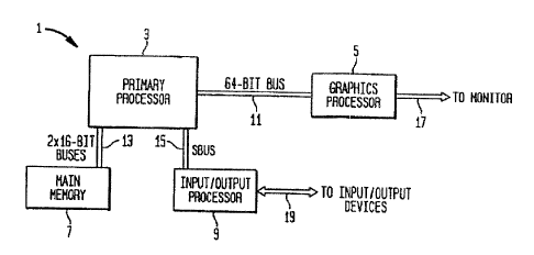
FIGURE 1. is a block diagram of computer system 1. Computer system
1 consists primarily of primary processor 3, graphics processor 5, main
memory 7 and input/output processor 9.
Primary processor 3 is a single 240 rnm2 chip, created using a 0.25-
micron photolithography process, with 10.5 million transistors which operates
at 300 MHz. Primary processor 3 is connected to graphics processor 5 by a 64-
bit bus 11 and ~~to main memory 7 by a pair of 16-bit buses 13. Primary
processor 3 is further connected to input/output processor 9 by a 32-bit SBUS
15. Graphics processor 5 is connected to a monitor (not shown) through
monitor connection 17. Input/output processor 9 transmits and receives data
through input/output device connections 19.
FIGURE 2 shows the major components of primary processor 3.
Primary processor 3 includes a 128-bit internal primary processor bus 21,
primary processor core 23, floating point unit (FPU) 25, a first vector
processing unit (VPUO) 27, a second vector processing unit (VPU1) 29, image
processing unit (IPU) 31, dynamic random access memory controller
(DRAMC) 33, S-bus interface (SIF) 35, direct memory access controller
(DMAC) 37, timer 39, interrupt controller (INTC) 41 and graphics processor
interface (GIF) 43.
-6-
CA 02298337 2000-04-06
FIGURE 3 shows the primary components of primary processor core
23. Primary processor core 23 is the CPU of computer system 1. Primary
processor core ~!3 has a 2-way superscalar architecture for enabling two
instructions to be executed per cycle.
The primary components of the primary processor core include a 32-bit
program counter 45. The program counter 45 contains a 64-entry branch
target address cache (BTAC) for use in performing branch predictions.
Primary processor core 23 predicts whether a conditional branch will be taken
and whether to prefetch code from the appropriate location. When a branch
instruction is executed, its address and that of the next instruction to be
executed (the chosen destination of the branch) are stored in the branch
target
address cache. 'This information is used to predict which way the next
instruction will lbranch when it is executed so that instruction prefetch can
continue.
The instn;~ction address from program counter 45 is transmitted to the
instruction translation look-aside buffer 47. Instruction translation look-
aside
buffer 47 is a table used in a virtual memory system for listing the physical
address page number associated with each virtual address page number.
Instruction translation look-aside buffer 47 is used in conjunction with
instruction cache 49 whose tags are based on virtual addresses. Instruction
cache 49 is an on-chip memory which is much faster than main memory 7 and
which sits in between primary processor core 23 and main memory 7.
Instruction cache 49 stores recently accessed data to speed up subsequent
accesses to the same data. Instruction cache 49 does this exclusively with
instructions.
A virtual address is presented simultaneously to the instruction
translation look-aside buffer 47 and to instruction cache 49 so that cache
access and the virtual-to-physical address translation can proceed in parallel
(the translation is done "on the side"). If the requested address is not
cached,
CA 02298337 2000-04-06
then the physical address is used to locate the requested data in main memory
7. Instruction cache 49 is a 2-way set associative cache. It receives physical
instruction addresses from the instruction translation look-aside buffer 47
and
the virtual instruction addresses from the program counter 45. The instruction
cache 49 receives cached instructions over BIU bus 51.
Instruction cache 49 also performs an instruction prefetch to minimize
the time primary processor core 23 spends waiting for instructions to be
fetched from main memory 7. Instructions following the one currently being
executed are loaded into a prefetch queue when the external busses are idle.
If
the primary processor core 23 executes a branch instruction, or receives an
interrupt, then the queue must be flushed and reloaded from the new address.
Instruction issue logic and staging register 53 receives the appropriate
instructions from the instruction cache 49 as determined by program counter
45, and then determines how to route the instructions to the appropriate one
of
six pipelines 65, 67, 63, 61, 71 and 73. Instruction issue logic and staging
register 53 can pass the instructions to either general purpose registers SS
or
the pipelines themselves.
General ,purpose registers 55 contain 32 128-bit general purpose
registers. This large number of registers allows for the handling of many
instructions in parallel. These registers are passed information from the
result
and move buses 57. General Purpose registers 55 can also transmit information
to, and receive information from, operand/bypass logic 59. An operand is an
argument of the machine language instruction set of primary processor core
23. Operand/bypass logic 59 can also receive information from the result and
move busses 57. This scheme allows operand/bypass logic 59 to take operands
from the pipelines for immediate use, thus improving performance. If
necessary, data can be stored back in the general purpose registers 55. The
operand/bypass logic 59 can also send appropriate data to scratchpad RAM 77
_g_
CA 02298337 2000-04-06
and data cache 75. Operand/bypass logic 59 can, of course, also pass
appropriate data vto the appropriate pipes of the pipelines.
Each of t:he 6 pipelines, pipelines 65, 67, 63, 61, 71 and 73, is a
sequence of functional units ("stages") for performing a task in several
steps,
like an assembly line in a factory. Each pipeline is passed operands from the
operand/bypass logic 59, or the instruction issue logic staging register 53,
and
passes its results to the result and move bus 57. Each functional unit of a
pipeline receives inputs from the previous unit and produces outputs which are
stored in an ouput buffer. One stage's output buffer is the next stage's input
buffer. This arrangement allows all the stages to work in parallel thus giving
greater throughput than if each input had to pass through the whole pipeline
before the next input could enter.
Four of the six pipelines are integer pipelines. The two primary integer
pipelines are IO pipeline 61 and I1 pipeline 63. These pipelines each contain
a
complete 64-bit ALU (arithmetic logic unit), a shifter, and a multiply
accumulate unit. The ALU performs addition, subtraction multiplication of
integers, AND, RJR, NOT, XOR and other arithmetic and Boolean operations.
I1 pipeline 63 contains a LZC (leading zero counting) unit. Pipelines IO 61
and I1 63 also share a single 128-bit multimedia shifter. These two pipes are
configured dynamically into a single 128-bit execution pipe per instruction to
execute certain 1.28-bit instructions, such as Multimedia, ALU, Shift and MAC
instructions.
LS pipe (loadlstore pipe) 65 and BR pipe (travel pipe) 67 also are
integer pipelines. LS pipe 65 contains logic to support 128-bit load and store
instructions which can access main memory 7. BR pipe 67 contains logic to
execute a branch instruction.
The remaining pipelines, C 1 pipe 71 and C2 pipe 73 support the two
coprocessors of system 1, floating point unit (FPU) 25 and vector processing
unit (VPUO) 27 (see FIGURE 2).
-9-
CA 02298337 2000-04-06
Floating point registers 69 are used to hold and pass data for C 1 pipe
71. This pipe contains logic to support the floating point unit 25 as a
coprocessor. The;re are 32 32-bit floating point registers 69 which are given
data by the operand/bypass logic 59.
C2 pipe 7:3 contains logic to support VPUO 27 as a coprocessor.
As noted above, all of the pipelines provide their output to result and
move bus 57. Re ult and move bus 57 passes the data back to operandlbypass
logic 59. Ope;rand/bypass logic 59 sends data that are finished with
computation to data cache 75 and the scratchpad R.AM 77.
Data cache 75 is a 2-way set associative cache which is 8KB in size.
Data cache 75 loads a necessary word from a cache line first (sub-block
ordering) and permits a hazard-free cache-line hit while a previous load is
still
under process (hit-under-miss).
The smallest unit of memory than can be transferred between the main
memory and the cache is known as a "cache line" or "cache block". Rather
than reading a single word or byte from main memory at a time, a whole line
is read and cached at once. This scheme takes advantage of the principle of
locality of reference: if one location is read, then nearby locations
(particularly
following locations) are likely to be read soon afterwards. It also takes
advantage of page-mode DRAM which allows faster access to consecutive
locations.
The output from data cache 75 is also buffered in write back buffer 79.
Data cache 75 h.as a write back protocol. Under this protocol, cached data is
on'1y written to main memory 7 when a later write runs out of memory in the
cache and forces out the previous cache. Write back buffer 79 is an 8-entry by
16-byte first-in-:First-out (FIFI) buffer ("FIFO"). Its use allows write
requests to
data cache 75 to be stored until the main internal primary processor bus 21 is
free. This scheme increases the performance of primary processor core 23 by
-10-
CA 02298337 2005-04-26
decoupling the processor from the latencies of main internal primary processor
bus 21.
Scratchpad RAM 77 is 16 KB of static RAM or (sRAM). As discussed
above, scratehpad RAM 77 is used as a double buffer to hide latency of main
memory 7 from the primary processor core 23. Scratchpad RAM 77 has
external DMA read and write capability for further speeding up access to main
memory 7. Response buffer 81 buffers scratchpad RAM 77 from primary
processor internal bus 21.
Memory management unit 83 supports virtual memory and paging by
translating virtual addresses into physical addresses. Memory management
unit 83 can operate in a 32-bit and 64-bit data mode. Memory management
unit 83 has a 48-double-entry full-set-associative address translation look-
aside buffer (TLB). In other words, it has 48 entries of even/odd page pairs
for 96 pages total. A page is a group of memory cells in RAM that are
accessed as parts of a single operation. That is, all the bits in the group of
cells
are changed at the same time. The page size for memory management unit 83
can range from 4 KB to 16 MB by multiples of 4. The virtual address size is
32-bits and the physical address size is 32-bits.
Memory management unit 83 sends updates via TLB refill bus 85 to
data address translation Look-aside buffer (DTLB) 87 and instruction address
translation look-aside buffer 47. These data refresh the tables in these
functional units. Instruction address translation look-aside buffer 47 has 2
entries and translation look-aside buffer 87 has 4 entries.
Data translation look-aside buffer 87 translates virtual data addresses to
physical data addresses. The physical data addresses are sent to either data
cache 75 or result and move bus 57.
Uncached accelerated buffer (UCAB) 88 .is also passed from memory
management unit 83. Uncached accelerated buffer (UCAB) 88 is a 2 entry by
4 by 16-byte buffer. It caches 128 sequential bytes of old data during an
-11-
, CA 02298337 2002-09-25
uncached accelerated load miss. If the address hits in the UCAB 88, the loads
from the uncached accelerated space get the data from this buffer.
Bus interface unit 89 connects primary processor main internal bus 21
to the BIU bus, 51 and thus to primary processor core 23.
An instruction set is the collection of machine language instructions
that a particular processor understands. In general, the instruction set that
operates a processor characterizes the processor. The instruction set for
computer system 1 has 64-bit words that conform to most of the MIPS III (and
partially to the MIPS IV) specifications. Specifically, the instruction set
implements all the MIPS III instructions with the exception of 64-bit
multiply,
64-bit divide, load-linked and store conditional statements. The instruction
set
fox computer system 1 implements the prefetch instructions and conditional
move instructions of the MII'S IV specification. 'The instruction set also
includes special primary processor Care instructions for primary processor
core 23, such as multiply/add (a 3-operand multiply, multiply-add instruction)
and 128-bit multimedia instructions. These instructions allow for the parallel
processing of 64-bits x 2, or 32-bits x 4, or 16-bits x 8 or 8-bits x 16. The
instruction set also includes I1 pipeline operation instructions, an interrupt
enable/disable instruction and primary processor core instructions. The
instruction set also includes instructions for 3 coprocessors. There is an
embedded coprocessor which is used for error checking in primary processor
core 23. A second coprocessor, COP 1, is FPtJ 25. This coprocessor is
controlled by instructions that are part of the primary processor instruction
set.
The third coprocessor, COP2, is vector processing unit (VPUO) 27, and is
controlled in two ways. In a macro mode, a program can issue macro-
instructions to primary processor core 23 to control vector processing unit
(VPUO) 27. These macro-instructions are part of the primary processor core
instruction set. The vector processing unit (VPUO) 27 also can be controlled
-12-
CA 02298337 2000-04-06
directly in a micro mode (see below). The macro mode and the micro mode
each has its own instruction set.
As discussed above, primary processor core 23 is the central processor
of computer system 1. This processor is supported by a series of additional
functional units in primary processor 3. Main internal primary processor bus
21 (FIGURE 2) ~;onnects primary processor core 23 to these functional units.
Main internal primary processor bus 21 has separate data and address buses.
The data bus is 128-bits wide. Main internal primary processor bus 21 has
8/16/32/64/128-bit burst access.
However, one functional unit is not connected to the main internal
primary processor bus 21. Referring back to FIGURE 2, floating point unit 25
is a coprocessor l;hat has both a 32-bit single-precision floating-point
multiply-
add arithmetic logical unit and a 32 bit single-precision floating-point
divide
calculator. This unit is tightly coupled to CPU core 23.
Vector processing unit zero (VPUO) 27 is a coprocessor used for non-
stationary geometry processing. This processing includes physical modeling
and other complicated matrix computations. Referring to FIGURE 4, vector
processing unit zero 27 consists of vector unit zero (VUO) 91, vector unit
memory zero (~'UMemO) 93, and vector interface zero (VIFO) 95. Vector
processing unit ;aero 27 is tightly coupled to primary processor core 23 by
VPUO coprocessor bus 97 which is separate from the main internal primary
processor bus 21. Thus the operation resources and registers for vector
processing unit ~:ero 27 can be operated directly from primary processor core
23 by using coprocessor macroinstructions. However, vector processing unit
zero 27 can also execute microprograrns independently of the primary
processor core 2:3.
Vector unit zero 91 is a floating-point vector processor unit. Vector
unit zero 91 has a built-in instruction memory, MircoMemO 99. MicroMemO
99 is 4 KB in size. MicroMemO 99 executes programs composed of 64-bit
-13-
CA 02298337 2000-04-06
microinstructions from 64-bit long instruction word (LIW) instruction sets.
These instructions are used by the vector unit zero core 101 to operate on the
data stored in the. VUO registers 103.
FIGURE 5 shows the vector unit zero 91 in more detail. Vector unit
zero 91 divides l:he 64-bit LIWs into an upper instruction field 105 of 32
bits
and a lower instmction field 107 of 32 bits. Vector unit zero 91 has pipelines
which are logically divided into upper execution unit 109 and lower execution
unit 111. Upper execution unit 109 has four 32-bit single-precision floating-
point multiply-add arithmetic logical units (FMAC ALUs), called FMACx
113, FMACy 115, FMACz 117, and FMACw 119. These four FMACs allow
simultaneous operation on the coordinates of a vertex of an object being
manipulated, whether the coordinates are XYZW, RGBA, STQR, or
NxNyNzNw. The lower execution unit 111 has one 32-bit single-precision
floating-point division/ square root calculation unit (FDIV) 121, as well as a
16-bit integer ALU (IALU) 123, a load/store unit (LSU) 125, a BRU 127 (a
unit for controlling program jumping and branching), and a random number
generator (RANDU) 129. This division allows each execution unit to be
addressed by a 3~2-bit instruction (the upper and lower instruction fields of
the
64-bit LIW). Thus, vector unit zero 91 can simultaneously perform a floating
point product-sum calculation and a floating-point division or integer
calculation.
Vector unit zero 91 has several different types of vector unit zero 91
registers 103 (FIGURE 4). Referring again to FIGURE S, these registers
include 32 128-bit floating-point registers 131, which are equivalent to four
single precision floating point values each. For a product-sum calculation,
two
128-bit registers can be specified as source registers and one 128-bit
register
can be specified as a destination register. These 32 128-bit floating-point
registers 131 also act as renamed data registers when 32 128-bit floating-
point
-14-
CA 02298337 2000-04-06
registers 131 acts as a coprocessor under the direct control of the primary
processor core 23.
Vector unit zero 91 also has 16 16-bit integer registers 133. These
registers are used for loop counters and load/store calculations. Vector unit
zero 91 also has a series of special registers 135. These special registers
include the four .ACC Registers, which are accumulators for the four FMAC
ALUs, the single 32-bit I Register where intermediate values are stored, the Q
register where the results of FDIV are stored, and the 23-bit R Register where
the random numbers generated by RANDU are stored. Vector unit zero 91
also has a series of control registers 137 which allow primary processor 3 to
use vector unit zero 91 as a coprocessor.
Vector processor unit zero 27 also includes vector unit memory zero 93
(FIGURES 4 and 5), which is structured in 128-bit (32-bit x 4) units. Vector
unit memory zero 93 is 4 KB in size and is connected to the LSU 125
(FIGURE 5) by a 128-bit wide bus. By using floating point registers 131 and
the vector unit memory zero 93 (built in data memory), vector processor unit
zero 27 can execute floating-point vector operations on 4 32-bit words
concurrently.
Vector processor unit zero 27 has two modes of operation. In the micro
mode, vector processor unit zero 27 operates as an independent processor by
implementing macro-instructions stored in MicroMemO 99. This mode allows
for highly efficient parallelism. Vector processor unit zero 27 also has a
macro mode. In the macro mode, the primary processor core 23 takes control
of vector processor unit zero 27 as a coprocessor, and can be controlled by
primary processor core 23 coprocessor instructions.
Vector interface zero (VIFO) 95 is a packet expansion engine that
implements a data unpacking function. Vector interface zero 95 can
efficiently recornstruct DMA-transferred packets of different data lengths for
vector unit memory zero 93. Data such as display lists is stored in main
-15-
CA 02298337 2000-04-06
memory 7 in formats optimized for fast data transmission and retrieval. These
formats are in dii:ferent data lengths than the actual data would be in its
native
state. Vector interface zero 95 allows such optimizations to occur without
primary processor core 23 having to spend computational power unpacking
these data.
Vector interface zero 95 can also start a microprogram. Thus a method
for operating vector processor unit zero 27 in micro mode is to send vector
interface zero 95 a DMA packet chain direct from scratchpad RAM 77 or main
memory 7 with a micro-instruction program, the vector data to be processed,
and the instruction to start the micro-instruction program.
FIGURE 6 illustrates in detail the tightly coupled connection between
vector processor unit zero 27 and primary processor core 23. Vector processor
unit zero 27 coprocessor bus 97 (FIGURE 4) is actually 3 separate
connections. These connections, shown in FIGURE 6, include a 128-bit bus
139 which allows primary processor core 23 to control vector processor unit
zero 27 floating point registers 131. These connections also include a 32-bit
bus 141 which gives primary processor core 23 control over integer registers
133 of vector processor unit zero 27, and a 32-bit bus 143 which gives the
primary processor core 23 control over upper execution unit 109.
Referring again to FIGURE 4, vector processing unit one (VPU1) 29 is
an independent processor used for stationary geometry processing. These
calculations include simple geometry transformations such as translation,
rotation, and other calculations such as certain light modeling calculations.
Vector processing unit one 29 consists of vector unit one (VU1) 145, vector
unit memory one (VM Meml) 147, and vector interface one {VIF1) 149.
Vector processing unit one 29 is connected to the main internal primary
processor bus 2 l~ .
Vector unit one 145 is a floating-point vector processor unit. Vector
unit one 145 has several elements shown in FIGURE 7. MicroMeml 151 is a
-16-
CA 02298337 2000-04-06
built-in instruction memory which is 16 KB in size. MicroMeml 151 executes
programs composed of 64-bit micro-instructions from 64-bit long instruction
word (LIW) instruction sets. The 64-bit LIWs can be divided into an upper
instruction field 1.53 of 32 bits and a lower instruction field 155 of 32
bits.
The pipelines of vector unit one 145 are logically divided into upper
execution unit 157 and lower execution unit 159. The upper execution unit
157 has four (4) 32-bit single-precision floating-point multiply-add
arithmetic
logical units (F1VIAC ALUs), called FMACx 161, FMACy 163, FMACz 165,
and FMACw 16'7. Lower execution unit 159 has one 32-bit single-precision
floating-point division/square root calculation unit (FDIV) 169, as well as a
16-bit integer AI~U (IALU) 171, a Load/Store Unit (LSU) 173, a BRU (a unit
for controlling program jumping and branching) 175, and a random number
generator (RANI~U) 177. Lower execution unit 159 also has an elementary
function unit (EFU) 179. Elementary function unit 179 performs exponential,
logarithmic and trigonometric functions. Elementary function unit 179 also
performs calculations on scalar or vector values and outputs a scalar value.
This division of pipelines between upper execution unit 157 and lower
execution unit 159 allows each execution unit to be addressed by a 32-bit
instruction (the upper and lower instruction fields of the 64-bit LIW). Thus
vector unit one t 45 can simultaneously perform a floating point product-sum
calculation and a~ floating-point division or integer calculation.
Vector unit one 145 also contains 32 128-bit floating-point registers
181. Each of these registers can contain four single precision floating point
values. For a product-sum calculation, two 128-bit registers can be specified
as source registers and one 128-bit register can be specified as a destination
register. Vector Unit One 145 also contains 16 16-bit integer registers 183.
These registers are used for loop counters and load/store calculations. Vector
unit one 145 also has a series of special registers 185. These special
registers
185 include four ACC Registers, which are accumulators for four FMAC
-17-
CA 02298337 2000-04-06
ALUs, a single :32-bit I Register where intermediate values are stored, a Q
register where the results of FDIV are stored, a 23-bit R Register where the
random numbers generated by RANDU are stored, and a P register which
records the value. generated by EFU 179. Vector unit one 145 also contains
control registers 187.
Vector unit one 145 also contains vector unit memory one 147, a date
memory which is structured into 128-bit (32-bit x 4) units. Vector unit
memory one 147 is 16 KB in size and is connected to load/store unit 173 by a
128-bit wide bus. By using floating point registers 181 and vector unit
memory one 14'1, the vector unit one 145 can execute floating-point vector
operations on 4 32-bit elements concurrently.
Vector processing unit one 29 (FIGURE 4) has only the micro mode of
operation. In i:he micro mode, the vector unit one 145 operates as an
independent processor by implementing micro-instructions stored in
MicroMeml 15 L. This mode allows for highly efficient parallelism as it
requires minimal. intervention by primary processor core 5.
Vector processing unit one 29 also contains a packet expansion engine, vector
interface one (V'.LF1) 149, for implementing a data unpacking function. Vector
interface one 149 can efficiently reconstruct DMA-transferred packets of
different data length. Data such as display lists are stored in main memory 7
in formats optimized for fast data transmission and retrieval. These formats
are in data lengl:hs different from the lengths of the actual data in its
original
state. Vector interface one 149 allows such optimizations to occur without
primary processor core 23 having to spend computational power unpacking
these data. Referring back to FIGURE 2, other specialized functional units
are included in primary processor 3. Graphics processor interface 43 is one
such specialized functional unit. Graphics processor interface 43 acts as the
interface between primary processor 3 and graphics processor 5 (FIGURE 1).
Graphics processor interface 43 is essentially an arbitration unit that can
-18-
CA 02298337 2000-04-06
decide whether 'to allow data from primary processor core 23 and vector
processor unit zero 27, as opposed to the vector processor unit one 29, to
pass
through to graphics processor 5 as these units generate parallel data streams.
Referring to FIGURE 8, graphics processor interface 43 contains
control logic and control registers 189, packing logic 191, and a 256-byte
embedded FIFO register 193 (first-in, first-out) that caches the inputted
data.
There is a second buffer 195 to hold the output of the graphics processor
interface 43 before sending these data to graphics processor S.
Graphics processor interface 43 allows three possible paths for data to
the graphics processor 5. The first path is PATH 1 197, which transfers data
from vector unit memory one 147 to graphics processor 5. PATH2 199 is the
data transfer path from vector interface one (VIF1) 149. PATH3 201 is the
direct data transfer path from the main internal primary processor bus 21 to
graphics processor interface 43, running through the embedded FIFO register
193. PATH3 201 is used when transferring data from main memory 7 or
scratchpad memory 77 to graphics processor 5. Graphics processor interface
43 arbitrates befiween transfer requests for the different paths, favoring
PATH1
197 over either F'ATH2 199 or PATH3 201.
Graphics processor 5 is passed data in a format consisting on two or
more graphics processor primitives, each headed by a GIFtag. The GIFtag is
128-bit in length, and denotes the size of the following GRAPHICS
PROCESSOR primitive and its data format (or mode). The GIFtag can
designate the register in graphics processor S to which the data should be
passed, thus specifying the data. Graphics processor interface 43 is also
passed one of three modes for graphics processor interface 43 to operate in:
PACK, REGLIST, and IMAGE. The first mode designates the need to
eliminate extraneous data from the primitive by using the GIF's packing logic
171, allowing graphics processor interface 43 to output a display list. The
second mode dcaignates that the graphics processor primitives being passed
-19-
CA 02298337 2000-04-06
are already in display list format. The third mode is used for transfernng
image
data such as texture data to graphics processor 5.
A detailed. description of image processing unit (IPU) 31 is shown in
FIGURE 9. Image processing unit 31 is an image data decompression
processor primarily involved with the interpreting and decoding of an MPEG2
bit stream. This operation generally is used to generate MPEG encoded
texture data for the rendering engine. Image processing unit 31 also includes
macro block decoder 203 for performing macro block decoding. This
processing is used to generate data upon which primary processor core 23
performs motion compensation. IPU 31 does not perform motion
compensation.
Image processing unit 31 also contains units for performing a set of
post processing functions. These units include color space conversion 205 and
dither and vector quantization 207. Color space conversion 205 converts the
YCrCb data of the MPEG2 data stream into RGBA format. YCrCb is a
chrominance/luminance color space model used in the British PAL television
standard. Y specifies luminance, Cr and Cb specify chrominance (blue/yellow
and red/cyan (or blue-green) components). Dither is used to smoothly convert
32-bit RGB format data to a 16-bit RGB format data. Vector quantization 207
uses the Color Look-Up Table (CLUT) to convert 16-bit RGB data to a 4-bit
or 16-bit index number used in color calculations such as texture mapping.
The Color Look Up Table (CLUT) is a table which establishes a
correspondence between the global palette (64K colors, for example), and the
subset of colors, i.e. the limited palette (made of 16 or 256 colors), used by
a
particular texture:.
Image processing unit 31 also contains two 128-bit FIFO registers 209
for input and output, two 64-bit registers, and two 32-bit registers.
FIGURE 10 shows a detailed description of S-bus interface (SIF) 35.
S-bus interface 35 is the interface unit to input output processor 9 (FIGURE
-20-
CA 02298337 2000-04-06
1). S-bus interface 35 is connected to input output processor 9 by a 32-bit
bus,
S-bus 15. S-bus 15 is a 32-bit bus for backward-compatibility reasons because
input output processor 9 is a 32-bit processor. S-bus interface 35 carries out
the necessary conversion of 128-bit data to 32-bit data with packing/unpacking
logic 211, storing the data to be packed and unpacked in SFIFO register 213.
S-bus interface 3:5 also contains control registers 215.
Another specialized functional unit shown in FIGURE 10 is direct
memory access controller (DMAC) 33 which has 10 channels for direct
memory transfers. Direct memory access allows memory transfers to occur
without the mediation of the primary processor core 23, thus saving processing
time. Memory transfer channels exist between main memory 7 and scratchpad
RAM 77. Memory transfer channels also exist between main memory 7
and/or scratchpad RAM 77 and vector interface zero 95, vector interface one
149, graphic processor interface 25, image processing unit 31, and the S-bus
interface 3 S. The DMA channels dealing with S-bus interface 3 S transfer
memory to S-bus 1 S in cooperation with the corresponding IOP DMAC 217.
Again, IOP DMAC 217 allows input/output processor core 219 to not be
involved in a memory transfer, such as to input/output processor memory 221.
Another specialized functional unit is the dynamic random access
memory controller (DRAMC) 37 (FIGURE 2) which controls the access to
main memory '1. In this embodiment, dynamic random . access memory
controller 37 controls Rambus direct random access memory, which is used in
the 32 MB of main memory 7. Rambus direct random access memory is a
specialized type of RAM allowing for very quick access. This special memory
technology allows very high bandwidth of data transfer at up to 600 MHz with
low latency. The fastest current memory technologies used by PCs (SDRAM),
on the other hand, can deliver data at a maximum speed of only about 100
MHz.
-21-
CA 02298337 2000-04-06
Another specialized functional unit is interrupt controller (INTC) 41
(FIGURE 2). Interrupt controller 41 signals device interrupts from each
device to primary processor core 23, and from DMAC 37.
Another specialized functional unit is timer 39 (FIGURE 2). Timer 39
contains four sep;~rate timers.
In operation, primary processor 3 takes advantage of the inherent
parallelism and differentiation of the functional units in its design. One
operation performed is patterned processing. Such processing involves images
that can be generated by control point and matrix operations. These operations
include perspective conversion, parallel light source calculation, creation of
secondary curved surfaces, and similar such calculations. In non-patterned
processing, on the other hand, images are generated by complex polygon
operations. Such operations include the simulation of deductive reasoning or
physical phenomena. Patterned processing generally is performed by vector
processing unit one 29, while non-patterned processing generally is performed
by primary core :Z3 in combination with vector processing unit zero 27.
There are several methods of taking advantage of this architecture. An
example is a race;-car game. In such a game, it is advantageous to calculate
the
position of the car's axles based upon physical modeling of the situation
(speed
of the car, angle of the car, surface and angle of the road, etc.). Primary
processor core 23 with vector processing unit zero 27 are responsible for
calculating the position of these axles. However, once these calculations are
made, the position of the tires and the body of the car are determined. The
object data, which would include the dimensions of the tire, car body, etc,
then
would be calculated based upon the control points generated by calculating the
position of the axles. Thus, the actual position of these objects would be
determined. Vector processor unit one 29 would be used to carryout these
relatively simpler calculations. Vector processor unit one 29 is much more
efficient at carrying out these simpler calculations. This division of
-22-
CA 02298337 2000-04-06
responsibility frees Primary processor core 23 to perform other operations.
Vector processor unit one 29 would then pass the display list generated to the
graphics processor 5 to be rendered. The display list is a data format which
defines one of seven primitives graphics processor 5 can draw, the conditions
under which each primitive is to be drawn, and the vertices of the primitives.
A second example of the advantages of the architecture of computer
system 1 is to display as a scene in a game, for example, a water drop falling
against a background of skyscrapers. The calculations involving the water
drop would be physically modeled. The Primary processor core 23 would
perform these calculations. The Primary processor core 23, with vector
processing unit :zero 27, then would generate a display list which would be
passed to graphics processor 5 to be rendered. Simultaneously, vector
processor unit one 29 would take object data of the skyscrapers from main
memory 7 and generate their position in the background using simple matrix
calculations. Primary processor core 23, with vector processing unit zero 27,
would also generate the matrices used to manipulate this object data. Thus,
each processor works separately on the calculations for which it is suited to
achieve parallelism.
Graphics processor 5 is a high performance rendering engine. The
primary function of graphics processor 5 is to take display lists which define
primitives, such as line or triangles (polygons), from the primary processor 3
and render these primitives in the frame buffer. Graphics processor 5 has
logic
to perform a variety of specialized calculations useful in rendering the
primitives. Graphics processor 5 can be described in functional units, as
shown in FIGURE 11.
The first functional unit is the Host I/F 301. HOST I/F 301 is an
interface between the main bus and priamry processor 3.
Setup/Rasterizing Preprocessor 303 is a functional unit that takes the
display list data of primitives and their vertices and gives out the value for
-23-
CA 02298337 2000-04-06
each pixel of such variables as RGBA, Z value, texture value, and fog value.
The rasterization uses a digital differential analyzer (DDA) algorithm, an
algorithm commonly used for line drawing.
The "A" i.n RGBA is the alpha channel. The alpha channel is the
portion of each pixel's data that is reserved for (usually) transparency
information. The. alpha channel is really a mask which specifies how the
pixel's colors should be merged with another pixel when the two are overlaid,
one on top of the other.
The pixel pipelines 305 processes a maximum of 16 pixels in parallel.
The pixel pipelines operate on 32-bit words. The pipeline performs such
processes as texvture mapping, fogging, and alpha-blending and determining
the final drawing color based on pixel information such as the alpha channel
and the coverage.
Memory I/F 307 reads and writes data from local memory 309. Local
memory 309 is 4 MB of RAM memory on graphic processor 5. Local
memory 309 contains the frame buffer, Z-buffer, texture buffer and CLUT.
Local memory 309 has a 1024-bit read port and a 1024 bit write port for
writing to and reading from the frame buffer, and a 512-bit port for texture
reading. The first two ports are associated with frame page buffer 311, and
the
last port with texture page buffer 313. Frame page buffer 311 can, for
example, simultaneously send and receive sixteen (16) 64-bit pixel
descriptions from Memory I/F 307, the 64-bit pixel descriptions including a
32-bit RGBA variable and a 32-bit Z variable. The texture page buffer can
pass sixteen (16) 32-bit texels a cycle to the pixel pipeline 305.
The frame buffer is an area where image data of drawing results are
stored. The frame buffer can store pixels in RGBA32 (8 bits/ 8 bits/ 8 bits/ 8
bits) RGB24 (8 bits/ 8 bits/ 8 bits), and RGBA16 (5 bits/ 5 bits/ 5 bits/ 1
bit)
formats. These: formats are all stored in 32-bit words. The pixels can be
designated in rwo kinds of coordinate systems. The primitive coordinate
-24-
CA 02298337 2000-04-06
system, which is the coordinate system of the drawing space, designates the
vertex coordinate: value during the drawing phase. The rectangular area in the
frame buffer where drawing actually takes place is defined in this space. The
window coordinate system is the system of coordinates which takes the upper
left hand corner of the frame buffer as its origin. The calculation of memory
addresses is based on these coordinates. The two coordinate systems are
intraconvertible by an offset value for x and y.
The Z coordinate is stored in the Z-buffer in 32, 24, and 16 bit formats.
In addition to the data formats defined for the frame buffer, the
IDTEX8 and IL)TEX4 formats are used in the texture buffer. These data
formats represent vectors pointing to a color in a color lookup table (CLUT).
The CLUT is used to convert a texel value from an index to RGBA color data.
The CLUT is stored in the CLUT buffer.
The PCR'TC (Cathode Ray Tube Control) 315 displays the contents of
the frame memory in the specified output format. Such formats include VESA
standard, NTSC, and PAL. The VESA standards are for computer monitors,
and include the: SVGA (Super VGA) standard. The NTSC standard for
television, used primarily in the United States, defines a composite video
signal with a refresh rate of 60 half frames (interlaced) per second. Each
frame
contains 525 lines and can contain 16 million different colors. PAL is the
television standard used in Europe.
In operation, graphics processor 5 receives a display list comprising
seven types of :primitives, including a point, a line, a line strip, a
triangle, a
triangle strip, a triangle fan and a sprite. The strips and fan are more
efficient
to draw as they utilize shard vertices. The sprite is an independent triangle
defined by two diagonally opposite corner vertices. A sprite is often used to
write text (e.g., a billboard in the background of a race game). The
primitives
in the display list will also give the drawing attributes of the primitive.
These
drawing attributes include shading method, texture mapping, fogging, alpha-
-25-
CA 02298337 2000-04-06
blending, anti-aliasing, texture coordinates, and context. Context informs
graphics processor 5 whether a primitive was generated by primary processor
core 23 in combination with vector processor unit zero 27 or by vector
processor unit one 29. Context, therefore, allows all of the other drawing
attributes to be set to one of two defaults previously set, thus saving
graphics
processor 5 procc;ssing time. This feature expedites switching between the two
sources, and thus. promotes efficient parallel processing of geometry data.
All
of these drawing attributes are set in drawing environment registers 317
(FIGURE 12).
Graphics processor 5 will then read the vertex information following
the primitive definition and drawing attributes, and begin the drawing
process.
The vertex information can be up to a set of four 32-bit coordinates. These
coordinates can :include, for example, the XYZW homogeneous coordinate of
each vertex, the RGBA color data of each vertex and texture coordinates
STQR (homogeneous coordinates). Other data potentially passed includes the
vector normals of a vertex of a polygon, Nx, Ny, Nz, Nw (used in calculations
such as light reflection). These vector normals are expressed in homogeneous
coordinates.
Homogeneous coordinates are coordinates under which the
transformation of scaling, rotation and translation can all be accomplished by
matrix multiplication without vector addition. This representation has clear
advantages because of its ease of manipulation. A point represented in
homogeneous coordinates is expressed with an additional coordinate to the
point. So, a two-dimensional point is represented in homogeneous coordinates
by three coordinates.
FIGURE 12 diagrams the processes applied to pixel data in graphics
processor 5 during setup (preprocessing) 319, the gradient (amount of change)
of the values of the variables received for the vertices of the primitives are
calculated. Values of the needed variables then are calculated along the drawn
-2 6-
CA 02298337 2000-04-06
lines outlining the primitives. Rasterizing 321 then takes place. This logic
implements a D:DA (Digital Differential Analyzer) which fills in the pixels
inside the primitive. The number of pixels written per cycle varies. With
texture mapping deactivated, 16 pixels are generated concurrently. When
texture mapping is activated, 8 pixels are generated concurrently. For
example,
associated with ;a pixel could be X, Y, Z values, R, G, B, A values, texture
coordinates and a fog value. All these values could pass into pixel pipelines
305 (FIGURE l l.) simultaneously.
In pixel pipelines 305, there are a series of optional graphic effects
applied to each pixel. These effects, shown in FIGURE 12, include texture
mapping 323, anti-abasing 325, fogging 327, pixel testing 329 and alpha-
blending 331.
Graphics processor 5 fills pixels in the following manner. In the case of
a triangle primitive, graphics processor 5 institutes a novel feature called a
"moving stamp." In the prior art, an arbitrary triangle was filled using a
rectangular stamp of a certain number of pixels by a certain number of pixels.
This stamp improved efficiency in calculating the values for the pixels to be
filled in the triangle by calculating the needed values for the first pixel
{in the
corner of the sta:mp). For each pixel thereafter calculated within the stamp,
the
calculations can be made in reference to the first pixel. Obviously part of
these calculations involves whether the pixel should be written to the frame
buffer at all (it should not if the pixel lies within the stamp but outside
the
triangle).
This algorithmic approach, as implemented in the prior art, has certain
drawbacks. The stamp is fixed in reference to an axis, such as the y-axis.
Thus, the stamp propagates along the x-axes of the triangle, until all of the
triangle of that ;y-region had been filled, and then the stamp would increment
up the y-axis by the height of the rectangle. The stamp would then start
moving again i:n the x-direction at the exact same x-coordinate. If the left
-27-
CA 02298337 2005-04-26
triangle side was at all sloped, therefore, many calculations were wasted by
checking to see if pixels should be written it to a part of the stamp well
outside
the triangle.
The "moving stamp'° by contrast is able, within certain
increments, to
shift the x-coordinate of its starting point when incrementing up the y-axis.
This shifting is a more efficient method for filling pixels within the
triangle.
For any given stamp over the edge of the triangle, the stamp is likely to have
less area outside the triangle.
Texture mapping 323 is performed on the pixels in the pipeline, if this
option has been activated. Texture mapping is in essence the "painting" of a
bitmap texture onto a polygon. Texture mappin;~ 323 for graphics processor 5
is shown in greater detail in FIGURE 13. The color of a given pixel written to
the frame buffer is determined by a combination of a texel color and the pixel
color derived from the rasterization process. 'fhe texel valor is determined
from either the S,T,Q or U,V. These coordinates both refer to a texture map, a
bitmapped image which contains texels (texture pixels) that are to be painted
onto the polygon.
The S,T,Q coordinates are the texture coordinate system, a
homogeneous system. The normalized coardina.tes s,t are derived from s=S/Q,
and t=T/Q 335. These coordinates are useful for applying texture mapping
with perspective correction. Perspective correction removes the distortion
that
appears when a texture map is applied to a polygon in space. Perspective
correction takes into account the depth of a scene and the spatial orientation
of
a -polygon while rendering texels onto the surface of a polygon. The S,T,Q
coordinates also assists in performing MIPMAI' calculations to determine the
correct LOD (Level of Detail). MIP mapping is a technique of precomputing
anti-abased texture bitmaps at different scales (levels of detail), where each
image in the map is one quarter of the size of the previous one. When the
texture is viewed from different distances, the correct scale texture is
selected
-28-
CA 02298337 2000-04-06
by the renderer so that fewer rendering artifacts are experienced, such as
Moire
patterns.
The U,V c;oordinate system is the texel coordinate system. The texture
coordinate system is converted at block 339 into the texel coordinate system
after the above calculations have been run. The texture map can be up to 1024
by 1024 texels. 'The LOD calculation 337 involves choosing the right level of
detail of the MIPMAP to be used.
After the selection of a S,T,Q derived U,V versus an original U,V value
341, the memory address calculation 343 is made. This is complicated by
attempts to address a texel outside the texture map. This problem can be
addressed by wrapping or repeating the texture, or clamping the texture such
that the texels on the edge are stretched out to the size needed to be
addressable by the address calculated.
This calculated address is then sent to the texture buffer 345, and a texel
value is sent to the Bit Expansion engine 347. If the texel value is not in a
format with 8 biia for each variable of RGBA (RGBA32 format), the format is
converted. Either RGBA16 or RGBA24 under goes a bit expansion, or a
IDTEX8 or ID'TEX4 format is referenced to the appropriate CLUT and
converted to an RGBA32 format.
The texell value is then sent on to filtering 349. Filtering options
include point s~~mpling, and bilinear interpolation in the MIPMAP itself.
Bilinear interpolation is an algorithm for interpolating image data in order
to
estimate the intensity or color of the image in between pixel centers. The
interpolated value is calculated as a weighted sum of the neighboring pixel
values.
There are seven possible MIPMAPs (seven levels of detail) derivable
from the primary texture map created by the game developer. Given certain
settings, it is possible to select linear interpolation between two adjacent
MIPMAPs after each have undergone bilinear interpolation in order to avoid
-29-
CA 02298337 2000-04-06
jumps between MIPMAPs in a game where the point of observation is
advancing. This is trilinear filtering.
A final value, a texel color, must be blended with the RGBA value of
the pixel (called a color fragment) by a function 351. Several functions are
possible, depending on the effect one wishes to generate. These functions are
MODULATE (the final value is the multiplication of the fragment value with
the texel value for each color), DECAL (the final value is the textel value),
HIGHLIGHT (the final color values are determined by Vv=Vf*Vt+Af, and
where Av=At+A.f), and HIGHLIGHT2 (the color values are calculated as in
highlight, but the final alpha value is the fragment alpha value). By
multiplication what is meant is A*B=(AxB)»7, and the result is clamped
between 0 and Oxff.
After texture is applied, a fogging effect may be applied at block 325
(FIGURE 12). This effect blends the set fog value (often gray) with the
RGBA value produced above. Fogging works such that the farther objects
become increasingly obscured. In other words, the contrast between the fog
color and objects in the image gets lower the deeper an object appears in the
scene. Fogging may be used to provide a back-clipping plane where objects
too distant to be seen clearly are removed to speed up the rendering of a
scene.
An anti-aliasing effect may be applied at block 327. Anti-aliasing is a
method of reducing or preventing aliasing artifacts when rendering by using
color information to simulate higher screen resolutions. In the graphics
processor 5, anti-aliasing is performed by taking the coverage value (ratio of
area which covers the pixel) produced by the DDA for each pixel on the edge
of a primitive, n~eating it as alpha, and performing alpha blending between
the
original primitive color (the source color) of the pixel and the destination
color
of the pixel (the; color currently in the frame buffer for the current
location).
Thus, when the coverage of a pixel is partial, the pixel behind it will blend
through. Therei:ore, graphics processor 5 implements anti-aliasing as a type
of
-30-
CA 02298337 2000-04-06
alpha blending, which is described further below. However, if one is
antialiasing, then one cannot be using alpha blending for other purposes.
Again referring to FIGURE 12, four pixel tests 329 are applied to the
pixel. The scissoring test tests if the pixels position is outside a defined
rectangle in the windows coordinate system. This test is not optional. A
failed
pixel is not processed any further. The Alpha test compares a pixel's alpha
value against a set value. The comparison can be set to any equality or
inequality. The effect of failing the test can also be controlled, with the
RGB,
A, and Z variables can be either not written or written depending on the
setting. The destination alpha test compares the alpha of the pixel to the
alpha
value of the pixel in the same position currently in the frame buffer. A
failed
pixel is not processed further. The depth test compares the Z value of a pixel
against the Z value of the corresponding pixel in the frame buffer. A failed
pixel is not pro<;essed further. This test essentially implements Z-buffering.
The other tests provide a game developer with a multitude of possible pixel
manipulations to create new graphical effects.
Alpha blending 331 generates an output color based on the depth test
output color generated above (Source Color or Cs), and the color of the pixel
in the same posiition in the frame buffer (destination color, or Cd). The
basic
calculation is
Final Output Color = {[(Cs,Cd or 0) - (Cs, Cd or 0)] * (As, Ad, FIXO)} + (Cs,
Cd, or 0)
where X * Y = (X x Y)»7. Thus a multitude of calculations are possible, all
allowing different sorts of blending between the source and destination color
in an amount depending on the value of alpha. In the specific case of
antialiasing, the formula reduces to Cs*As+Cd*(Ox80 - As).
-31-
CA 02298337 2000-04-06
Graphics processor 5 will then send these values for a final formatting
at block 333. The RGB values of the pixel will be dithered if they are to go
to
the frame buffer in RGBA16 format. If after alpha blending, the value of RGB
is beyond the accepted value then a color clamp is applied to bring the values
into range. Alpha values for pixels can be corrected to a preset value. The
pixels are then format converted, packed into a number of bits specified by
the
developer (RGB.A32, RGBA24, or RGBA16). The pixel values of RGBA are
written to the frame buffer, and the pixel Z values are written to the Z
buffer.
Cathode ray tube controller 315 (FIGURE 11 ) will then convert the frame
buffer into the appropriate standard signal for a monitor.
Input output processor (IPO) 9 (FIGURE 1 ) serves multiple functions in
the computer system l.. Input output processor 9 is a complete 32-bit CPU in
its own right. This architecture provides backward compatibility with earlier
game systems. Input output processor 9 also manages all input and output data
for the primary processor 3, except for the output to the video monitor. Input
output processor 9 can deal with USB, IEEE1394, and other standard input
and output data.
Sound processor unit (SPU2) is a sound synthesis processor, which is
composed of tu-o cores and equipped with local memory and external I/O.
The two cores have the following functions: ( 1 ) reproduce the sound data
input
successively from the host; (2) process voices; (3) output the voice-processed
sound data to the host successfully; and (4) perform digital effects
processing.
The two cores, COREO and CORE1, are functionally equivalent, and are
connected to each other such that the output of COREO is the input to COREI,
and the output of COREl is the final mixed sound signal. The functional
blocks of the SPU include: ( 1 ) the host interface; (2) the register RAM; (3)
the
COREO; (4) the CORE1; (5) the memory interface; (6) the local memory; and
(7) the output block. The Host Interface is connected by the a 32-bit bus to
the
IOP. The register RAM sets the function of the SPU2. All the registers are
-32-
CA 02298337 2000-04-06
16-bits in width. The local memory is 2 Mbytes of RAM. The local memory
is divided into four functional areas: (1) the sound data input area; (2) the
sound data output area; (3) the waveform data area; and (4) the digital effect
work area. The sound data input area has data written in by the host, and
outputted to the ;iPU2 cores. The sound data output area is buffer in this
area,
and is read by the host. The digital effect work area is in fact two areas
used
by the cores as scratch space for digital effect delay processing.
The preferred embodiments described above include numerous
variations and combinations which are within the spirit and scope of the
invention. The fi~regoing description should be understood as an illustration
of
the invention, therefore, rather than as a limitation. The scope of the
invention
is described by the following claims.
-33-