Note: Descriptions are shown in the official language in which they were submitted.
CA 02298479 2002-05-09
SPIRAL SLOT LINE RESONATOR
BACKGROUND OF THE INVENTION
1. Field of the Invention
The present invention relates to a dielectric resonator, an inductor, a
capacitor, a dielectric filter, and an oscillator which are produced by
forming an
electrode on a dielectric substrate, and a communication device using the
above.
2. Description of the Related Art
Microstrip line resonators or slot line resonators are known as resonators
employing dielectric substrates for use in a microwave band or a millimeter
wave
band.
A conventional slot line resonator is a single resonator constructed using a
linear slot line having a length of half a wavelength. Since the slot line
resonator
has continuous electrodes surrounding slots, electromagnetic energy at the
surroundings of the slot line resonator is highly efficiently enclosed.
Therefore,
when the slot line resonator is implemented in a high-frequency circuit, there
is an
advantage in that less interference with other circuits occurs.
Conductor loss of the resonator using the conventional slot line whose
cross-sectional view is shown in Figs. 19A and 19B is described.
The electrode, which constitutes the slots, is divided into three regions,
i.e.,
an electrode edge region, an electrode top face region, and an electrode
bottom
face region. Computation of the conductor loss is performed on each region
using
a simulator. The following Table. 1 shows the ratio of the conductor loss in
the top
CA 02298479 2000-02-10
- 2 -
and bottom face regions of the electrode to the total conductor loss in a slot
line in
which the sizes shown in Fig. 19A are employed.
TABLE 1
RATIO OF LOSS OF TOP AND
SLOT WIDTH BOTTOM FACES OF ELECTRODE TO
TOTAL CONDUCTOR LOSS
l0ym 77%
25 E~m 84
50 «m 88
100 ym 90
Regardless of the slot width, loss in the top and bottom faces of the
electrode occupies the major portion of the total conductor loss. When, for
example, the slot width is 100 E~m, approximately ninety percent of the total
loss
occurs at the top and bottom faces of the electrode.
Although dielectric loss occurs in the slot line resonator, the conductor loss
is the dominant factor.
As described above, the conductor loss in the top and bottom faces of the
electrode occupies the major portion of the total conductor loss caused by the
so-
called "skin effect". The skin effect occurs because of a nonuniform
distribution of
current inside the electrode, in other words, because of greater current
density at
CA 02298479 2000-02-10
- 3 -
the surface of the electrode.
SUMMARY OF THE INVENTION
Accordingly, it is an object of the present invention to provide a dielectric
filter, an inductor, a capacitor, and an oscillator which effectively reduce
conductor
loss due to the skin effect and which constitute a dielectric resonator having
a
high unloaded Q-factor (Qo), as well as a communication device using the
above.
To this end, according to a first aspect of the present invention, there is
provided a dielectric resonator including a slot line constructed by providing
a slot
electrode having a spiral slot at an external face of a dielectric layer or
inside of
the dielectric layer and a shield conductor provided at a predetermined
distance
from the slot electrode. The slot line is employed as a resonant line.
Hereinafter, an end of the spiral provided at the outermost circumference
thereof is denoted as an exterior end while an end of the spiral provided at
the
innermost circumference thereof is denoted as an interior end. Fig. 17 shows
the
electromagnetic field distribution in a linear slot line and directions of the
currents
induced by the magnetic field. Broken curved lines represent the direction of
the
magnetic field, solid curved lines represent that of the electric field, and
linear
arrows represent that of currents in the slot electrode induced by
electromagnetic
waves propagating in the slot. A remarkable point is that the directions of
currents
flowing through the electrode on both sides of the slot are mutually opposite.
The
present invention constructively takes advantage of this effect. That is, by
forming
the slot line into a spiral shape, currents flowing through the electrode
between
neighboring slots are counterbalanced whereby conductor loss is reduced.
As a typical slot line, the slot line in which one end thereof is a short-
circuit
CA 02298479 2000-02-10
- 4 -
end and the other end thereof is an open end may be employed. In this case, it
is
preferable that the line length be ~.~/2 or ~.~/4 when the resonant wavelength
of the
resonator is denoted as ~,9. Since the direction of the magnetic field is
unchanged
between nodes of a standing wave in the resonator, the direction of the
current
induced in the slot electrode is also unchanged in the section. When the
directions of the currents through the electrode on both sides of the entire
slot are
unchanged, by forming spiraled slots, the current counterbalance always occurs
between neighboring slots. When a node of the standing wave exists in the
resonator, by forming spiraled slots, there is a part in which the current
density is
increased. Therefore, it is preferable that the resonator (the slot) length be
~,~/2 or
~.~/4.
The width of the slot line may be wider in the proximity of the short-circuit
end thereof than in the proximity of the open end thereof. The current density
of
the electrode on both sides is maximum at the short-circuit end thereof and
zero
at the open end thereof. By forming spiraled slots, since the slots
accompanied
by the electrode whose current density is different are disposed closely,
though
the counterbalance occurs, the current counterbalance effect does not cause
the
current value to be zero. Accordingly, it is preferable that the slot width be
gradually changed so that the current counterbalance occurs over the entire
slot,
whereby, as a result, the current value approaches zero.
In the dielectric resonator, the width of the slot line may be changed through
substantially the entire body thereof. Furthermore, the width of the slot line
may
be changed in a curved manner in accordance with the position in the
longitudinal
direction thereof.
In -the dielectric resonator, one end of the slot line may be a short-circuit
CA 02298479 2000-02-10
- 5 -
end and the other end thereof may be an open end thereby employing the slot
line
as a quarter-wavelength resonant line. Because of this, the entire line length
becomes shorter and the area occupied by the slot line is also further
reduced.
In the dielectric resonator, an exterior circumferential end of the slot line
may be a spiral short-circuit end, thereby employing the slot line as a
quarter-
wavelength resonant line or a half-wavelength resonant line. That is, the
quarter-
wavelength resonator line is obtained in a case where the interior end is an
open
end, while the half-wavelength resonator line is obtained in a case where the
interior end is a short-circuit end. Both cases make the value of the magnetic
field intensity at the exterior end of the spiral slot line be maximum.
In the dielectric resonator, the slot electrode may have two spiral slots
whose exterior circumferences are connected to each other having a
substantially
point-symmetry relationship therebetween and the interior circumferential ends
of
the two slots are individually employed as short-circuit ends of the slot
line.
Since this construction makes the symmetry point have a maximum electric
field value and makes each of the interior ends of the two spiral slot lines
individually have maximum magnetic field values, the electromagnetic field is
highly efficiently enclosed.
In the dielectric resonator, the slot electrode may have two spiral slots
whose exterior circumferences are connected to each other so as to have a line-
symmetry relationship therebetween and the interior circumferential ends of
the
two slots are individually employed as short-circuit ends of the slot line.
This
construction makes the position on the symmetry line to have a maximum
electric
field value, and makes the distance between neighboring slot lines wider.
In the dielectric resonator, the slot may have a spiral shape obtained by
CA 02298479 2000-02-10
- 6 -
deforming the entire body thereof into a substantial rectangle, which can
reduce
the area occupied by the spiral slot for the dielectric substrate.
According to a second aspect of the present invention, there is provided an
inductor including a slot line constructed by providing a slot electrode
having a
spiral slot at one of an external face of a dielectric layer and inside of the
dielectric
layer and a shielding conductor provided at a predetermined distance from the
slot electrode. In the inductor, an end of the slot line is a short-circuit
end and the
length of the slot is not more than one-eighth of a transmission wavelength of
the
slot line.
In the inductor, the width of the slot line may be wider in the proximity of a
short-circuit end thereof than in the proximity of an open end thereof, which
makes the current density distribution in the longitudinal direction of the
slot line
uniform, whereby the total conductor loss is reduced.
According to a third aspect of the present invention, there is provided a
capacitor including a slot line constructed by providing a slot electrode
having a
spiral slot at one of an external face of a dielectric layer and inside of the
dielectric
layer and a shielding conductor provided at a predetermined distance from the
slot electrode. In the capacitor, an end of the slot line is an open end and
the
length of the slot is not more than one-eighth of a transmission wavelength of
the
slot line.
In the capacitor, the width of the slot line may be wider in the proximity of
a
short-circuit end thereof than in the proximity of an open end thereof, which
makes the current density distribution in the longitudinal direction of the
slot line
uniform, whereby the total conductor loss is reduced.
According to a fourth aspect of the present invention, there is provided a
CA 02298479 2000-02-10
dielectric filter including a signal input/output unit and any one of the
above
dielectric resonators.
According to a fifth aspect of the present invention, there is provided an
oscillator including a negative resistance circuit and any one of the above
dielectric resonators. In the oscillator, the negative resistance circuit and
the
dielectric resonator are coupled.
According to a fifth aspect of the present invention, there is provided a
communication device including at least one of the above described inductor,
the
above described capacitor, the above described dielectric filter, and the
above
described oscillator.
BRIEF DESCRIPTION OF THE DRAWINGS
Figs. 1A and 1 B are diagrams showing the construction of a dielectric
resonator according to a first embodiment of the present invention;
Fig. 2 is a diagram showing the construction of a dielectric resonator
according to a second embodiment of the present invention;
Fig. 3 is a diagram showing the construction of a dielectric resonator
according to a third embodiment of the present invention;
Fig. 4 is a diagram showing the construction of a dielectric filter according
to a fourth embodiment of the present invention;
Figs. 5A and 5B are diagrams showing constructions of dielectric filters
according to a fifth embodiment of the present invention;
Figs. 6A and 6B are diagrams showing constructions of an inductor and a
capacitor according to a sixth embodiment of the present invention;
Fig. 7 is a diagram showing an example of applying the dielectric resonator
CA 02298479 2000-02-10
_ g _
to a fin line;
Fig. 8 is a diagram showing a pattern of a rectangular spiral slot;
Figs. 9A, 9B, and 9C are diagrams showing another pattern of a
rectangular spiral slot;
Fig. 10 is a diagram showing the construction of an oscillator;
Fig. 11 is a plan view showing another construction of a dielectric resonator;
Figs. 12A and 12B are graphs showing changing patterns of the slot width
of the dielectric resonator;
Fig. 13 is a plan view showing another construction of the dielectric
resonator;
Fig. 14 is a plan view showing further another construction of the dielectric
resonator;
Fig. 15 is a sectional view showing still another construction of the
dielectric
resonator;
Fig. 16 is a block diagram showing the construction of a communication
device;
Fig. 17 is a diagram showing an example of an electromagnetic field
distribution in a straight slot line;
Fig. 18 is a diagram showing a magnetic field intensity distribution in the
proximity of the slot line; and
Figs. 19A and 19B are diagrams showing construction parameters which
are used for computation of conductor loss in the slot line.
Fig. 20 is a diagram showing the construction of a dielectric duplexer
according to the present invention;
CA 02298479 2000-02-10
- 9 -
DESCRIPTION OF THE PREFERRED EMBODIMENTS
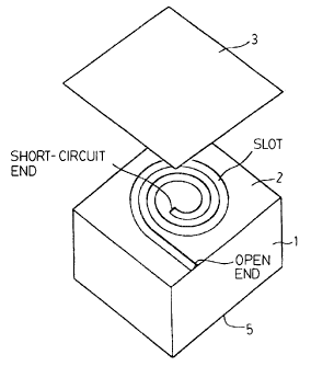
The construction of a dielectric resonator according to a first embodiment of
the present invention is described with reference to Figs. 1A and 1 B. Fig. 1A
is a
perspective view showing primary parts of the dielectric resonator, and Fig. 1
B is
a perspective view showing a distribution of currents flowing in the proximity
of
slots. The slots are regions between parts of an electrode in which the
dielectric
body is exposed. In Figs. 1A and 1 B, a dielectric substrate 1 has a slot
electrode
2 having spiral slots at the top face thereof, and has a shielding electrode 5
formed on substantially the entire bottom face thereof. An upper shielding
electrode 3 is provided at a predetermined distance above the dielectric
substrate
1. A slot line, the upper shielding electrode 3, the shielding electrode 5, an
air
layer between the slot line and the upper shielding electrode 3, and a
dielectric
layer between the slot line and the shielding electrode 5 constitute a
resonator. In
the peripheral region of the slot line, an electromagnetic field is
distributed in the
dielectric layer as well as in the outer air layer.
As shown in Figs. 1A and 1 B, the interior end of the slot is a short-circuit
end while the exterior end thereof is an open end. When the resonant
wavelength
of the resonator is denoted as ~.9, it is preferable that the length of the
slot be ~,~/4
or ~.~/2. The reason for this is described hereinbefore.
When the wavelength of an electromagnetic wave distributed in the air layer
is denoted as ~o, it is preferable that the upper shielding electrode 3 be
provided
within ~.~/2 from the slot electrode 2 in view of shielding effect. Such a
provision of
the upper shielding electrode 3 blocks the radiation of waves toward the
outside
and the incidence of waves from the outside, thereby acting as a dielectric
resonator.
CA 02298479 2000-02-10
- 10 -
In Fig. 1 B, solid arrows represent the direction of a current induced at an
exterior circumference of the spiral, and broken arrows represent the
direction of a
current induced at an interior circumference thereof. Because the currents,
which
have opposite directions, flow so closely between neighboring slots, currents
flowing between neighboring slots are counterbalanced over the entire slot
line.
Therefore, the conductor loss is greatly reduced between neighboring parts of
the
slot line.
In order to prove the above counterbalance effect, the intensity of a
magnetic field which is caused by three parallel slot lines in close proximity
to one
another, as shown in Fig. 18, is computed using a finite element method (FEM).
In Fig. 18, the upper part of the diagram is a graph showing the distribution
of the
magnetic field intensity; the middle part of the diagram is a cross sectional
view
showing the three parallel slot lines; and the lower part of the diagram is a
plan
view of the three parallel slot lines. In this case, it is assumed that
electromagnetic waves having the same phase are excited in each of the three
slot lines. The values of construction parameters as shown in Fig. 18 are
used.
As is obvious from the upper part of the diagram, currents flow extremely
densely at edges of the electrodes while the current density decreases
drastically
further from the edges. The magnetic field intensity in a region "B" is
noticeably
less than that in a region "A". The region "A" is a region which does not have
a
slot further outside. Accordingly, it can be understood that the current
density
between neighboring slots becomes very low, whereby the conductor loss is
greatly decreased.
To~ confirm the above-efifect, the inventors produced a resonator having a
structure shown in Fig. 1. The open-end of the resonator was connected with an
CA 02298479 2000-02-10
- 11 -
open-end of an another resonator to form a single resonator. The width of the
slot
was 20,u m and the resonant frequency of the respective resonator was 70GHz.
Then, unloaded Q of the resonator was 100.
Also, a comparative resonator was produced. The comparative resonator
utilized a slot line whose width was 20,ccm and length was the same as the
combined slot lines of the above-resonator, but the slot was straight. The
unloaded Q of the comparative resonator was 40.
The construction of a dielectric resonator according to a second
embodiment of the present invention is described with reference to Fig. 2.
Fig. 2
is a perspective view showing primary parts of the dielectric resonator. A
dielectric substrate 1 has a slot electrode 2a having spiral slots formed at
the top
face thereof. As shown in Fig. 2, the slot has an open end at the interior end
thereof, which is circular and has no electrode, and has a short-circuit end
at the
exterior end thereof. When the wavelength in the slot line is denoted as ~.9,
the
slot length is ~.~/4, thereby constituting a quarter-wavelength resonator.
Upper and lower shielding electrodes 3 and 4 are provided above and
below the dielectric substrate 1, respectively, within a half-wavelength from
the
slot electrode 2a. The provision of the upper and lower shielding electrodes 3
and
4 blocks the radiation of waves toward the outside and the incidence of waves
from the outside, thereby acting as a dielectric resonator.
By making the exterior end of the spiral slot a short-circuit end, since a
maximum magnetic intensity point exists outside of the spiral, it is easy to
couple
the slot with an external circuit. For example, by providing a coaxial probe
in the
proximity of this short-circuit end, magnetic field coupling between the
coaxial
probe and the slot line occurs.
CA 02298479 2000-02-10
- 12 -
The lower shielding electrode 4 is not necessary when the dielectric
substrate 1 in Fig. 2 has a shielding electrode formed on substantially the
entire
bottom face thereof in the same manner as the case in Figs. 1 A and 1 B.
The construction of a dielectric resonator according to a third embodiment
of the present invention is described with reference to Fig. 3. In Fig. 3, a
dielectric
substrate 1 has a slot electrode 2b at the top face thereof. An upper
shielding
electrode 3 is provided at a predetermined distance above a dielectric
substrate 1.
The slot electrode 2b with spiral slots, the dielectric layer of the
dielectric
substrate 1, and the outer air layer constitute a slot line.
The slots of the spiral electrode 2b have a configuration in which two slots
whose rotating directions are identical are connected, while having a point-
symmetrical relationship. This slot line has short-circuit ends at two
interior ends
B1 and B2 of the spiral slots. The length of the slot line is ~.~/2 so that
the
symmetry axis A is equivalent to an open end, whereby a half-wavelength
resonator is constituted.
By thus providing two spirals, in proximity to each other, whose rotating
directions are identical, the direction of the current induced at a slot in
the
proximity of the region indicated by "A", and the direction of the current
induced at
neighboring slots on both sides of the slot are counterbalanced. Therefore,
the
conductor loss due to the skin effect at a part having these three slots in
proximity
to each other can be reduced. Accordingly, compared with the spiral slot line
having a single spiral shape, the space occupied by the slots on the
dielectric
substrate can be reduced, which enables the entire device to be further
miniaturized.
By further increasing the dielectric constant of the dielectric substrate due
CA 02298479 2000-02-10
- 13 -
to a decrease in the length represented by "L" in Fig. 3, more electromagnetic
energy is enclosed in the dielectric substrate, which reduces the radiation of
electromagnetic energy toward the outside.
The construction of a dielectric filter according to a fourth embodiment of
the present invention is described with reference to Fig. 4.
A dielectric substrate 1 has a slot electrode 2c at the top face (as observed
in the Fig. 4) thereof and has a slot electrode 7, whose pattern is the same
as that
of the electrode slot 2c (mirror-symmetry), at the bottom face thereof. By
providing the slot electrodes 2c and 7 at both faces of the dielectric
substrate, a
slot line having a double slot structure is constructed. The slot electrode 2c
has a
structure in which two spirals, whose rotating directions are opposite, are
connected so as to have a line-symmetry relationship between these two
spirals.
This slot line has short-circuit ends at interior ends B1 and B2 of the two
spirals
and the line length is ~.~/2 so that a symmetry axis A' is an equivalent open-
end,
thereby constituting a half-wavelength resonator.
The dielectric substrate 1 has a coplanar line formed by the pattern of the
slot electrode 2c on the top face and the central conductor of the coplanar
line is
disposed so as to be perpendicular to slots at the region A'. The coplanar
line has
a ground electrode at the bottom face thereof. This construction enables
electric-
field coupling between the coplanar line and the slot line to occur, which
makes a
dielectric filter having the coplanar line as a signal input/output unit. This
filter
functions in the same manner as the equivalent circuit of a band erase filter
(BEF)
provided with a one-stage trap resonator between a transmission line and a
ground.
As shown in Fig. 4, when two slots are disposed so as to have a line-
CA 02298479 2000-02-10
- 14 -
symmetry relationship, since a region in which the exterior circumferences of
two
slots are connected to each other is separated from a spiral slot region, it
is easy
to provide the input/output circuit to the line of the symmetry axis.
Accordingly,
matching between the filter and the input/output circuit is increased.
The construction of a dielectric filter according to a fifth embodiment of the
present invention is described with reference to Figs. 5A and 5B.
In Fig. 5A, resonators R1 and R2, constructed using slot lines, are
individually identical to the resonator shown in Fig. 4. By providing the two
slot
lines closely, magnetic-field coupling occurs. Thus, a two-stage resonator
constitutes a dielectric filter having bandpass characteristics where ports #1
and
#2 using coplanar lines are employed as input/output units.
In Fig. 5B, resonators R1, R2 and R3, constructed using slot lines, are
individually identical to the resonator shown in Fig. 4. By providing the
three slot
lines close to one another in the above mentioned order, magnetic-field
coupling
occurs at a region of one slot line in close proximity to another slot line.
Thus, a
three-stage resonator constitutes a dielectric filter having bandpass
characteristics
where ports #1 and #2 using coplanar lines are employed as input/output units.
The construction of an inductor and a capacitor according to a sixth
embodiment of the present invention is described with reference to Figs. 6A
and
6B.
In Fig. 6A, a dielectric substrate 1 has a spiral slot electrode 2d at the top
face thereof and an upper shielding electrode 3 at a predetermined distance
above the dielectric substrate 1. When the wavelength of the slot line is ~.9,
the
length of the slot line is determined to be not more than ~.~/8. The interior
end of
the slot line is a short-circuit end.
CA 02298479 2000-02-10
- 15 -
When the time-average of the electrical energy We of the slot line and the
time-average of the magnetic energy of the slot line Wm in the construction
shown
in Fig. 6A satisfy the relationship Wm » We, the slot line functions as a
lumped
circuit inductance element when observed from the exterior end of the slot
line.
In Fig 6B, the length of the slot line is determined to be not more than ~.~/8
and the interior end of the slot line is an open end. The rest of the
construction in
Fig. 6B is the same as that in Fig. 6A. In the construction in Fig. 6B, the
relationship Wm « We is obtained, and the slot line functions as a lumped
circuit
capacitance element when observed from the exterior end of the slot line.
Fig. 7 is a partial perspective view showing the construction of a dielectric
resonator according to a seventh embodiment of the present invention. In Fig.
7,
the dielectric substrate 1 is disposed inside of a rectangular waveguide
whereby a
fin line is constructed. The dielectric substrate 1 has a slot electrode 2f at
the top
face thereof, as observed in the Fig. 7. The pattern of the slot electrode 2f
is
identical to the corresponding slot electrode shown in Fig. 3. This structure
enables the fin line including the dielectric resonator to be constructed, and
also
enables the dielectric resonator to function as a bandpass filter which allows
a
resonant frequency signal of the dielectric resonator to be passed.
In the above embodiments, examples are described in which a spiral slot
whose curvature monotonically varies is formed in a generally circular region.
Alternatively, the slot may have a rectangular spiral shape which can be
formed in
a generally rectangular region as shown in Fig. 8. Accordingly, such a shape
enables a space for a slot line having the required length to be secured even
though the amount of space is limited, which can reduce the area occupied by
the
spiral slot for the dielectric substrate.
CA 02298479 2000-02-10
- 16 -
Fig. 9A shows one modification of the rectangular spiral slot shown in Fig.
8; Fig. 9B shows the bend in the encircled part of the spiral slot in Fig. 9A;
and Fig.
9C shows the bend in the encircled part in Fig. 8. When the slot width of a
straight line part of the slot line and that of a bent part of the slot line
are the same,
as shown in Fig. 8, since the interior current path L;~ of the slot and the
exterior
current path Lo~, of the slot produce a physical path difference, the
occurrence of a
spurious mode is promoted. Accordingly, as shown in Fig. 9B, the slot width of
the bent part is decreased to less than that of the straight line part so that
the path
difference between the interior path L;~' of the slot and the exterior path
Lot' of the
slot becomes smaller. Such a pattern can prevent the spurious mode from
occurring.
Fig. 10 is a perspective view showing the construction of an oscillator. In
Fig. 10, a dielectric substrate 1 has a slot electrode 2g formed on the top
face
thereof and a shielding electrode 5 on substantially the entire bottom face
thereof.
An upper shielding electrode, which is not shown in Fig. 10, is provided at a
predetermined distance above the dielectric substrate 1. The slot electrode 2g
has a resonator part and an oscillation circuit part. In the resonator part,
two
spiral slots having a line-symmetry relationship, as shown in Fig. 4, are
provided,
whereby the resonator using a slot line is constituted. In the oscillation
circuit part,
a coplanar line, or another line which is changed into a coplanar line using a
line-
transition device, is connected to a negative-resistance circuit built by an
FET
(field effect transistor) and the like. By connecting the negative-resistance
circuit
to the resonator built by the above slot lines, a band reflex oscillator is
constructed.
The construction of another dielectric resonator having uneven slot widths
+s described with reference to Figs. 11 and 12.
CA 02298479 2000-02-10
- 17 -
Fig. 11 is a plan view showing the dielectric resonator on a dielectric
substrate. In the example shown in Fig. 3 and the like, it is assumed that the
slot
width of the slot line is even at any position of the longitudinal direction
thereof.
However, in the example shown in Fig. 11, the slot width becomes wider from
each open-end towards each short-circuit end. Apart from the pattern formed on
a slot electrode 2h, the other components are identical to the corresponding
ones
shown in Fig. 3.
When the slot width of the slot line is even from one end to the other, the
current density becomes a maximum at the short-circuit end and approximately
zero at the equivalent open end. Therefore, by widening the slot width of the
slot
line from the open end toward the short-circuit end, the current density
distribution
of the slot line in the longitudinal direction becomes even, which prevents
the
current from becoming dense. As a result, the total conductor loss decreases
and
the unloaded Q factor further increases.
Even when the slot width is changed, by maintaining the distance between
neighboring slots at a generally regular interval regardless of the position
in the
longitudinal direction of the slot, as shown in Fig. 11, the counterbalance
action,
which is caused by the currents flowing through two neighboring lines over the
entire length of the slots, can be maintained.
Figs. 12A and 12B show relationships between the width of the slot line and
the position in the longitudinal direction of the slot. In an example
represented by
broken lines "a" in Fig. 12A, when the slot width is 1 at the short circuit
end and
the slot width at the middle of the slot line (which is the equivalent open-
end) is
0.5, the slot width is linearly changed in between. Such a linear change of
the slot
width facilitates the design and formation of the pattern of the slot
electrode.
CA 02298479 2000-02-10
- 18 -
In an example represented by solid lines "b" in Fig. 12A, the slot width is
linearly changed from the middle of the slot line up to the proximity of the
short-
circuit end thereof and the slot width is constant therefrom. When the slot
width
becomes wider towards the center of the spiral, as shown in Fig. 11, it is
difficult to
secure space for the slot line having the required length. However, by
providing
an upper limit of the slot width at around the proximity of each end of the
slot line,
the slot line having a predetermined length can be constructed without causing
the area occupied by the slot line to increase.
In an example represented by solid lines "b" in Fig. 12B, a function of the
slot width in the longitudinal direction of the slot line is a pattern which
is
expressed with a curve from the middle of the slot line to the short-circuit
end. In
this example, the function is an upward convex. Generally, when the current
density of the slot line is observed macroscopically, the intensity is
trigonometrically distributed along the longitudinal direction of the slot
line so that
the current density is Zero at the open end and a maximum value at the short-
circuit ends. On the other hand, when the slot line is in a spiral shape and
the
current density distribution is microscopically observed, there is a component
which expands in the lateral direction. This lateral-direction component
exponentially changes in the lateral direction. Accordingly, it is considered
that
the current density in the longitudinal direction of the slot line can be
expressed
with an overall function obtained by combining the trigonometric function with
the
exponential function. The pattern represented by "b" in Fig. 12B is obtained
by
considering the above current density distribution. It is difficult to express
the
above function using a formula. The pattern of the slot line can be obtained
using
a simulation or the like so that the current density distribution is made
uniform and
CA 02298479 2000-02-10
- 19 -
a predetermined line length is obtained in a limited space.
The pattern represented by broken lines "a" in Fig. 12B is identical to the
pattern represented by "a" in Fig. 12A. As represented by "a" and "b" in Figs.
12A
and 12B, by causing the slot width to be a pattern which changes in accordance
with the position in the longitudinal direction of the slot, since the values
of
currents flowing through two neighboring slots are close, an effective
increase in
the current counterbalance action is achieved.
Fig. 13 is a plan view showing a dielectric substrate having another
dielectric resonator. In examples shown in Figs. 1A and 1 B and the like, the
slot
width of the slot line is even at any position of the longitudinal direction
thereof. In
the example shown in Fig. 13, the slot width becomes wider from the open end
toward the short-circuit end. Apart from the pattern formed on the slot
electrode,
the other components are identical to the corresponding ones shown in Figs. 1
A
and 1 B. Such a construction causes the conductor loss to decrease as well as
the unloaded Q factor to further increase, thereby functioning as a quarter-
wavelength resonator.
Fig. 14 is a plan view of a dielectric substrate of further another dielectric
resonator. In this dielectric resonator, a spiral slot line has a short-
circuit end at
the exterior circumferential end thereof and an open end at the interior
circumferential end. In the examples shown in Fig. 2 and the like, the slot
width of
the slot line is even at any position of the longitudinal direction thereof.
In the
example shown in Fig. 14, the slot width becomes wider from the open end
toward the short-circuit end. Apart from the pattern formed on the slot
electrode,
the other components are identical to the corresponding ones shown in Fig. 2.
Such a construction also causes the unloaded Q factor to increase, thereby
CA 02298479 2000-02-10
- 20 -
functioning as a quarter-wavelength resonator.
Regarding a capacitor or an inductor, in the same manner as in the case of
the dielectric resonator, by making the slot width of the slot line wider from
the
open end toward the short-circuit end based on the construction shown in Fig.
6,
the inductor and the capacitor having further reduced loss can be obtained.
Likewise, regarding a filter, in the same manner as in the case of the
dielectric resonator, by making the slot width of the slot line wider from the
open
end toward the short-circuit end based on the construction shown in, for
example,
Fig. 4 or Fig. 5, the filter having further reduced insertion loss can be
obtained.
In each embodiment described above, the slot electrode is constructed by
being provided between the dielectric layer of the dielectric substrate 1 and
the
dielectric layer of the outer air. However, for example, as shown in a cross
sectional diagram in Fig. 15, the slot electrode may be provided so that the
electromagnetic field between the two dielectric layers of the upper arid
lower
electrodes is enclosed. That is, in Fig. 15, the construction of a dielectric
substrate 1, a slot electrode 2 on the top face thereof, and a shielding
electrode 5
on the bottom face thereof are identical to the corresponding components of
the
above-described embodiments. Furthermore, another dielectric layer of a
dielectric substrate 1' is provided on the slot electrode 2 and has a
shielding
electrode 6 formed on the outer face thereof. In this case, the dielectric
constants
of the dielectric substrates 1 and 1' may be or may not be identical.
Fig. 20 shows one example of a duplexer according to the present invention.
The filter shown in Fig. 5A is used as a transmitting filter and a receiving
filter.
The signs Tx, Rx ANT denote transmitting signal input port, receiving signal
output port and transmitting/receiving input/output port respectively.
CA 02298479 2000-02-10
- 21 -
Fig. 16 is a block diagram showing the construction of a communication
device using the above dielectric filter and oscillator. A mixer MIXa
modulates a
frequency signal, which is obtained by causing a frequency divider
(synthesizer)
DIV to divide an oscillating frequency generated at an oscillator OSC, with a
modulating signal. A signal of transmission frequencies among the modulated
signal is allowed to pass by a band pass filter BPFa and is power-amplified by
an
amplifier AMPa, and the amplified signal is transmitted via a duplexer DPX
from
an antenna ANT toward the outside. A band pass filter BPFb allows a signal of
received frequencies of an input signal from the duplexer DPX to pass, and an
amplifier AMPb amplifies the received signal. A mixer MIXb mixes a frequency
signal from a band pass filter BPFc with the received signal into an
intermediate
frequency signal IF.
The dielectric duplexer having the construction in Fig. 20 may be used as a
duplexer DPX. The dielectric filters having the constructions in Figs. 5A and
5B
may be used as band pass filters BPFa, BPFb, and BPFc shown in Fig. 16, and
the oscillator having the construction shown in Fig. 10 may be used as the
oscillator OSC. These dielectric filters and oscillator are surface-mounted on
a
circuit substrate of a high frequency circuit unit. Thus, a compact
communication
device can be constructed.
Regarding the above inductor and capacitor, in the same manner as in the
case of the dielectric filters and oscillator, a communication device is
constructed
by having inductors and capacitors surface-mounted on a circuit substrate of
the
high frequency circuit unit.