Note: Descriptions are shown in the official language in which they were submitted.
CA 02298557 2000-O1-27
WO 99105507 PCTlUS98115724
COHERENT INTERACTION OF OPTICAL RADIATION
BEAMS WITH OPTICAL-ELECTRONIC MATERIALS OF
GENERALIZED CRYSTAL SYI~IETRY
REFERENCE TO PRIOR APPLICATIONS
This application claims the benefit of Priority
Application Serial No. 60/653,977, filed July 28, 1997.
BACKGROUND OF THE INVENTION
The present invention relates to the coherent
interaction of optical radiation beams with ions or
molecules in solids, and to the choice of propagation
direction and light polarization relative to the crystal
symmetry axes of the solid, and more particularly to
optimize the optical-electronic interaction effects in
materials with generalized crystal symmetry.
DESCRIPTION OF THE RELATED ART
A variety of optical-electronic applications are
based on the coherent interaction of optical radiation
beams or fields with ion-doped or molecular crystals of
various types; these interactions include optical
coherent transients, spectral hole burning, and
spatial-spectral holography (also called time- and
space-domain holography). Devices based on these
concepts are used in optical data storage, real-time
optical signal processing, quantum computers, and other
coherent computers where the coherent interaction of
multiple radiation beams is enhanced, enhanced data
erasure in coherent computers, and optical data routing
and have applications to computers, communications
CA 02298557 2000-O1-27
WD 99105507 PCTIUS981i5'724
2
networks, the Internet and other networks, time delays in
RADAR, and numerous other applications.
Natural and synthetic optical materials have a wide
range of potential crystal lattice symmetries. (A
well-known catalog of all crystal space groups is the
International Tables for Crystallography, Edited by Theo
Hahn, published by the International Union of
Crystallography, D. Reidel Publishing Co.) Within these
materials, active ions or molecules occupy crystal
'lattice sites' that can be cataloged into subsets, with
members of each subset having identical surroundings and
having similar resonant frequencies for coupling to
optical radiation (the members of each subset are said to
be ~crystallographically-equivalent'); each
crystallographically-equivalent subset of lattice sites
may contain ions or molecules with a finite number of
different spatial orientations. The optical transitions
of electrons in the ions or molecules can be described by
two quantum energy levels and a transition dipole moment
.
In general, these transition dipole moments have a
plurality of different spatial orientations, according to
the different orientations of the crystallographically-
equivalent sites noted above. Light beams, on the other
hand, must have single optical propagation directions and
polarization states relative to the crystal, with the
consequence that the light polarization will have a
plurality of different spatial relationships with
otherwise identical ions or molecules.
When resonant coherent interactions occur, the
interaction of the optical field and the two-level
quantum systems can be characterized by the optical Rabi
frequency:
_ p'~o
~R
CA 02298557 2000-O1-27
WO 99!05507 PCT/US98/15724
3
where p is the electric dipole moment with
components pi = <1 ~ pi ~ 2> and Eo is the optical electric
field vector. (Similar expressions apply for magnetic
dipoles and magnetic optical fields. In extreme
situations a power-broadened version of the above
equation applies.)
The Rabi frequency is determined not only by the
magnitudes of the transition dipole moment and of the
optical field, but also by the projection of one onto the
IO other (vector projection or scalar product).
Consequently, when arbitrarily polarized radiation is
propagated through such materials, the coherent
interaction of the field and the crystalline matter will
induce macroscopic polarization oscillations at a
plurality of different optical Rabi frequencies.
The presence of multiple optical Rabi frequencies
generally reduces the effectiveness of the optical-
electronic device due to consequent complex transient
material polarization behavior and the optical
interference or beating of the associated optical signal
amplitudes radiated by the material. Such interference,
for example, can in turn limit the optical-electronic
system bandwidth and hence the response time and data
handling capability in the optical-electronic
application. The interference may also reduce the
optical diffraction efficiency, i.e., the signal
selection or deflection efficiency in such devices as
optical data routers for optical communications networks
and wavelength-division multiplexing systems.
To avoid the deleterious effects of this multiple
frequency interference, while still being able to
optimize other system parameters, it is necessary to
design a procedure for obtaining 'single-Rabi-frequency'
behavior in a generalized situation. The small group of
materials that have only a single site orientation can
readily exhibit single frequency behavior. Here,
CA 02298557 2000-O1-27
WO 99105507 PCTIUS98115724
4
however, we show that a wider range of materials,
including multi-site materials, can exhibit
single-Rabi-frequency behavior under the conditions that
we have discovered.
The crystalline compound, Y,A15012 (yttrium aluminum
garnet - "YAG"), which has been used by several research
groups for device demonstrations, is a particularly
complicated optical material, and its behavior serves to
illustrate the problems arising from the interference
l0 effects described above, and also to illustrate our
invention. In past applications, light was propagated
along the so-called crystallographic <111> direction of
YAG, a propagation direction that does not yield
single-Rabi-frequency behavior. There are one hundred
sixty (160) ions per unit cell of the YAG lattice (the
unit cell is the fundamental building block of the
crystal). When rare earth ions are substituted as active
ions for yttrium at the dodecahedral lattice sites, there
are six (6) crystallographically-equivalent sites, each
with a differently-oriented local environment. Hence,
there are six different directions for the individual
transition dipoles of the active rare earth ions. For an
arbitrary optical propagation direction and for arbitrary
optical polarization, there will be six different Rabi
frequencies.
In principle, one could eliminate the degradation in
performance arising from the presence of multiple Rabi
frequencies by choosing a different material with an
appropriately high symmetry that restricts the sites to
a single orientation. In general, though, that
high-crystal-symmetry approach to obtaining a single Rabi
frequency does not work for device applications, since
one must simultaneously optimize many other material
properties, including the optical coherence or dephasing
time, inhomogeneous optical line broadening, transition
probability, persistence of spectral hole burning,
CA 02298557 2000-O1-27
WO 99105507 PCTIUS98/15724
dependence of all of these properties on the applied
magnetic field, and dependence of all of these properties
on temperature. Satisfying all of these demands in a
single material is at best a difficult challenge, even
5 when no other restrictions on material selection exist
(such as the restriction to a single site orientation).
This 'high-symmetry' approach has so far proven to be
impractical. Conventionally, the optical material had to
be chosen from a small subset of available materials,
most or all of which do not have a single set of
identically-aligned and oriented crystallographically-
equivalent dipoles; that represents a sacrifice in
potential bandwidth, diffraction efficiency, and
performance.
The following example shows the difficulty of the
high-symmetry single-site-orientation approach. The
choice of a single-site material would make it relatively
simple to achieve a single optical Rabi frequency in the
transmission of a radiation beam or field, and could
thereby increase the effectiveness of the device, but it
also significantly reduces the optical transition
probability in many cases and even reduces it identically
to zero in many cases of interest. It also restricts the
choice of materials that may be used to a very small
fraction of the totality of optical materials that might
be otherwise considered for use in the particular
application. Since many interesting optical materials
with multiple site orientations have other
characteristics that are superior to those of materials
with the high crystal symmetry necessary to give a single
site orientation, it is advantageous to solve the single
Rabi frequency problem in a generalized way, so that
optical-electronic devices can benefit from the use of
materials with multiple site orientations specifically
and from a far wider range of materials generally.
CA 02298557 2000-O1-27
WO 99105507 PCTJUS98115724
6
SIT1~1ARY OF THE INVENTION
Accordingly, it is an object of the present
invention to provide a technique for eliminating the
deleterious effects of multiple Rabi frequencies on the
speed and bandwidth characteristics of optical-electronic
interaction effects for materials with generalized
crystal symmetry.
It is another object of the present invention to
provide a technique for reducing material polarization
interference in optical-electronic interactions.
It is a further object of the present invention to
provide a technique for optimizing optical transition
probability in optical-electronic interactions for a wide
range of optical materials.
It is a further object of the present invention to
provide a technique for optimizing diffraction efficiency
in optical-electronic interactions for a wide range of
optical materials.
Additional objects, advantages, and novel features
of the present invention will become apparent to those
skilled in the art from this disclosure, including the
following detailed description, as well as by practice of
the invention. While the invention is described below
with reference to preferred embodiments, it should be
understood that the invention is not limited thereto.
Those of ordinary skill in the art having access to the
teachings herein will recognize additional
implementations, modifications, and embodiments, as well
as other fields of use, which are within the scope of the
invention as disclosed and claimed herein and with
respect to which the invention could be of significant
utility.
In accordance with the present invention, to reduce
undesirable interferences and thereby increase the
effectiveness of optical-electronic interactions, a beam
of radiation, e.g. a coherent light beam, (or multiple
CA 02298557 2000-O1-27
WO 99/05507 PCT/US98/15724
7
beams of radiation? is propagated through a material
having a generalized crystal symmetry with specific light
propagation direction and polarization state specified
relative to the conventional axes of crystal symmetry of
the material (linear or elliptical polarization). Since
the material has a generalized crystal symmetry, the
material's transition dipoles will have several
independent transition directions; that is, the material
will have a crystal lattice structure with a plurality of
unaligned, differently-orientated dipoles at
crystallographically-equivalent sites.
The invention involves a procedure for determining
a suitable optical propagation direction and polarization
state that projects equally on the respective directions
of the transition dipoles, or more typically a subclass
of the dipoles, and which is orthogonal to the respective
directions of any remaining transition dipoles, i.e. all
dipoles of the original subset not within the subclass of
dipoles. The radiation beam is polarized, linearly or
otherwise, relative to the axes of symmetry to equally
project onto each of the dipoles within the subclass of
dipoles. Beneficially, the propagating radiation beam is
polarized identically with respect to each of the dipoles
within the subclass and orthogonally to dipoles outside
the subclass of transition dipoles, and accordingly,
equally projects onto each of the dipoles within the
subclass of transition dipoles.
The propagation of the polarized radiation beam
through the material actively excites ions in the
subclass of dipoles so as to induce them to oscillate
cooperatively. The dipoles of the ions outside the
subclass preferably are not oscillated. Advantageously,
each of the dipoles in the subclass are oscillated at the
substantially same Rabi frequency and have a
substantially equal transition intensity.
CA 02298557 2000-O1-27
WO 99105507 PCTIUS98/15724
8
The relationship of the propagation direction and
polarization to the axes of crystal symmetry will change
dependent upon the selection of dipoles forming the
subclass of dipoles. In any event, the subclass of the
dipoles is selected such that there exists a special
direction, specified relative to the conventional axes of
crystal symmetry, that projects equally on the respective
transition dipoles within the subclass and is orthogonal
to the respective transition dipoles of the remainder of
the dipoles.
According to the invention, a system for propagating
a beam of radiation through a material having a plurality
of unaligned, differently-orientated
crystallographically-equivalent transition dipoles
includes a monochromatic frequency-agile radiation
emitter (or several emitters) for emitting a beam (or
multiple beams) of radiation along a path towards the
optical-electronic material. An optical controller or
encoder for each beam made up, for example, of an
acousto-optical, electro-optical, or other modulator or
combination of modulators imposes amplitude or phase
information on the beam of radiation (or prepares the
beam to manipulate another of the several radiation
beams). A possibly-two-dimensional deflector makes
adjustments in the beam direction as may be required by
the optical-electronic device application. Input optics
direct the radiation beams) to the crystalline material
where the radiation-material interaction critical to
device performance occurs. A polarizer is configured (or
polarizers are configured) to polarize each emitted
radiation beam in a direction such that the radiation
beam polarization(s) has (have individually)
substantially the same projection with respect to
multiple dipoles making up a subclass of transition
dipoles. In some cases, the typically very small angles
between multiple incident radiation beams can be freely
CA 02298557 2000-O1-27
WO 99/05507 PCTIUS98/15724
9
varied while maintaining the desired single Rabi
frequency behavior (the garnet example illustrates that) ;
in other cases the small angles typically involved
between several beams mean that the conditions can be met
simultaneously to a good approximation. Beyond the
optical-electronic material, there are output optics and
an array of radiation detectors or other independent
receiving channels such as optical fibers for the
signals.
BRIEF DESCRIPTION OF THE DRAWINGS
The various advantages and merits of the invention
will become more apparent as a detailed description of
the embodiments thereof is given with reference to the
accompanying drawings in which:
Figure 1 shows the relative orientations of the six
orientationally-inequivalent but crystallographically-
equivalent dodecahedral sites in the crystal lattice of
Y3A15012. This is a particularly complicated system that
has been chosen to illustrate the general procedure that
is applicable to any crystalline material (there is a
non-denumerable number of possible crystalline materials
to which these concepts apply - limits are described
below) .
Figure 2 shows an example of an unoptimized coherent
interaction (where beating reduces signal amplitude) and
shows two different examples, wherein identical optical
fields are used, of optimized coherent interaction for
the material of Figure 1.
Figure 3 depicts an optical-electronic device
configured to transmit radiation through the generalized
optical material in accordance with the optimized
material interaction of the present invention.
CA 02298557 2000-O1-27
WO 99/05507 PCTIUS98/15724
- 10
DESCRIPTION OF THE INVENTION
Figure 1 depicts an optical material 90 having a
particularly complicated crystal symmetry. The material
90 is garnet, which serves to illustrate the application
of this invention to the symmetry properties of a
generalized material, as previously noted in the
discussion of the Background Art. The chemical formula
for garnet crystals is A3BZC3c71z - The A ions occupy six
crystallographically-equivalent but orientationally-
inequivalent versions of this single type of
crystallographic site with orientations labeled 10-60,
each with dodecahedral point symmetry. The garnet
material is doped with rare earth ions which typically
substitute for the A ions and experience the same
dodecahedral symmetry with respect to the six sites
10-&0.
Each of the sites 10-60 has local orthogonal axes,
x, y and z, but as the lozenge symbols in Fig 1
illustrate, these three directions are not equivalent.
In Figure 1, the local axes are shown only for site 10.
However, those skilled in the art will recognize that the
local axes of each of the sites 10-60 will have a
different orientation since, unlike in materials with a
single set of identically aligned and oriented
crystallographically-equivalent sites, the material 90
has a complicated crystal symmetry and accordingly,
differently-oriented, unaligned, but crystallo-
graphically-equivalent sites; these six orientations are
determined by the so-called Oh or Ia3d symmetry
(standard international crystallographic symbols).
According to convention, the use of the material 90
in optical-electronic devices is not optimum due to the
plurality of different orientations of these six sites
arising from the garnet crystal symmetry or to another
plurality in the generalized case. More particularly,
radiation directed through the material 90 in the
CA 02298557 2000-O1-27
WO 991055U7 PCT/US98/15724
. 11
conventional manner will oscillate ions at the sites
10-60 at six different optical Rabi frequencies which
will result in optical interference and transient
material polarization behavior such that the
effectiveness of the device will be substantially
degraded as compared to a device with identically aligned
and oriented sites. This optical interference is
illustrated by the observed optical nutation shown in
Figure 2 line C.
However, if the Rabi frequencies could be made equal
at each of the nutating sites 10-60, the effectiveness of
an optical-electronic device incorporating material 90 as
the radiation interaction medium, could be substantially
improved and the associated transient material
polarization behavior simplified. By reducing the
optical interference caused by the respective sites 10-60
nutating at different Rabi frequencies, the system
bandwidth and diffraction efficiency could be
substantially enhanced.
In accordance with the present invention, this can
be accomplished by properly selecting the radiation
propagation direction and the radiation polarization
state specified relative to the conventional axes of
crystal symmetry of the material 90.
More particularly, the transition dipoles at each of
the sites 10-60 necessarily lie along either the local x,
y, or z axes for different sites and electronic states of
the material. Hence, when the electric vector of
radiation for electric dipole transitions or the magnetic
vector for magnetic dipole transitions has a non-zero
projection on the dipole, it will induce nutation of the
transition dipoles at the sites 10-60.
For an even-electron rare earth ion like Tm3' in the
garnet material used for illustration here, the possible
electronic states of the material involved in the optical
transitions are labeled by conventional symmetry
CA 02298557 2000-O1-27
WO 99/05507 PCTJUS98/15724
12
designations rl, r2, r3, and r4. The symmetry
transformation properties of the transition electric
dipoles together with the symmetry properties of the two
quantum states involved in the transition select either
the px, pY, or px dipole corresponding to the local axes
shown in Fig 1. Since the local x, y and z axes of each
of the six crystallographically-equivalent sites 10-60
are oriented differently from each other site, six
different orientations of dipoles corresponding to the
six different sites 10-60 are likewise present.
Hence, if a beam of radiation is directed through
the material 90 in the conventional manner, the electric
or magnetic field vector will typically have unequal
projections with respect to each of the six orientations
of transition dipoles. This will necessarily result in
unequal transition intensities for each of the sites
10-60 and consequently different Rabi or nutation
frequencies. Conventional propagation of the radiation
beam along the so-called crystallographic <I11> direction
farces this multiple Rabi frequency situation to occur.
However, in accordance with the present invention,
by properly configuring the beam of radiation transmitted
through the material 90, the Rabi or nutation frequencies
for at least a subclass of the totality of sites, IO-60
in the present illustration, can be made equal;
simultaneously, sites outside the chosen subclass are
made inactive. Stated another way, by choosing the
proper light propagation direction and light polarization
state relative to the axes of crystal symmetry, a
cooperative oscillation at a single Rabi frequency can be
achieved in the material 90.
Taking the axes of crystal symmetry of the material
90 into consideration, the radiation field direction can
be chosen so that all sites being excited by the
radiation have the same projection of the radiation field
onto the transition dipoles. Hence, whereas the use of
CA 02298557 2000-O1-27
WO 99!05507 PCTlUS98l15724
13
conventional techniques in, for example, optical coherent
transient applications and spatial-spectral holography,
will result in the dipole vectors precessing at different
rates under the driving influence of the radiation beam
or field thereby causing unwanted cancellations of the
material polarization (i.e., the sum of all dipole
vectors), by properly choosing the radiation field
direction in such applications in accordance with the
teachings herein, the dipole vectors will precess at
substantially, if not exactly, the same rates when driven
by the radiation beam or field and no cancellations of
the material polarizations of the precessing dipole
vectors will occur.
The proper selection of the radiation field or beam
configuration is established by first determining a
direction that equally projects on a subclass of the
dipoles (corresponding to a subclass of the sites 10-60
for the garnet material case) and which is perpendicular
to the remaining dipoles (at the remaining sites 10-60 in
the garnet case). This direction has a specific
relationship (or perhaps several specific relationships)
to the axes of crystal symmetry of the material. The
radiation beam is then propagated perpendicular to and
polarized along this direction (in the linear
polarization case) so as to equally project on the dipole
moments.
Thus, the radiation beam or field will be polarized
at an equal angle with respect to each of the transition
dipoles in the subclass of dipoles that are actively
oscillated. The radiation beam or field may be linearly
or otherwise polarized, so long as the radiation beam or
field equally projects onto the dipoles within the chosen
subclass of dipoles. When the electric or magnetic
radiation field vector is in the proper direction, the
radiation field vector, i.e., the radiation polarization,
has the same projection relative to all transition
CA 02298557 2000-O1-27
WO 99/05507 PCTIUS981I5724
14
dipoles in the subclass of dipoles and hence identical
transition intensities.
Accordingly, for the specific case of the garnet
material as indicated in Figure 1, and for Tm3' ion
transitions between states of rl and rz symmetry, by
propagating a radiation beam or field along the A axis
(known in the specific garnet case as the
'crystallographic <100> direction') and polarizing the
beam cr field along the axis B (known in the specific
garne~ case as the 'crystallographic <O10> direction'),
the radiation field will induce transitions at identical
Rabi frequencies for the four sites l0-40. It will be
noted that the four-fold crystal symmetry axis in this
case is along axis B. Alternatively, a three-fold crystal
symmetry axis lies along axis D of Figure 1.
Accordingly, by propagating a radiation beam or field
along axis E and polarizing the beam or field along axis
D, the induced transitions for the three sites 10, 40 and
&0 will be at identical Rabi frequencies (if the dipole
is along y); the other sites are not active.
Figure 2 depicts the light emission intensities over
time caused by propagating and polarizing the radiation
beam cr field as described above with respect to special
directions specified relative to the crystal symmetry
axes and corresponding in this case to axis B (line A in
Fig. 2; or D (line B in Fig. 2), as depicted in Figure 1.
A third line on the graph depicts the transition
intensi ty over time caused by a conventionally configured
radiation beam or field with respect to the crystal
lattice structure of material 90 of Figure 1. Figure 2
indicates the beneficial effects of the single Rabi
frequency behavior resulting from the implementation of
the inventive technique described herein.
In each of the above described exemplary
applications of the present invention, the dipoles of the
sites 10-60 that are actively oscillated exhibit the
CA 02298557 2000-O1-27
WO 99/05507 PCT/iTS98/15724
desired cooperative properties under coherent
illumination. In applications utilizing coherent
interaction, the above described technique allows optical
materials that may have otherwise beneficial properties
5 to be utilized. It should be noted that the above
reflects the results of testing carried out on 0.1%. Tm3+
doped Y3A15012 . The 3H6 ( 1 ) to 3H4 ( 1 ) transition,
i . a . ,
793.374 nm in a vacuum, is an electric dipole transition,
and the transition dipole between these states is
10 directed along the local y axis.
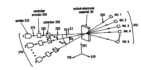
Figure 3 depicts a simplified exemplary system
configuration in accordance with the present invention.
As will be understood by those skilled in the art, the
depicted configuration will typically also include other
15 elements such as collimators, lenses, etc., inserted
along the radiation beam path as may be desirable for the
particular implementation. For the garnet example, the
crystal lattice structure of the material 90 includes
sites 10-60 as have been described above with reference
to Figure 1.
The system includes a radiation beam emitter 210 (or
an array of such emitters) which is shown as a laser
source but could be another radiation source as may be
suitable for the intended application. The radiation
beam 215 emitted from the emitter 210 is propagated in
the desired direction by the controller 220 which could,
for example, be an acousto-optical modulator (AOM) or
other suitable control device for propagating the
radiation beam 215 along the proper path with respect to
the selected axis of crystal symmetry of the material 90
and modulating its intensity, frequency, and phase. The
propagating beam 225 is output from the controller 220 to
a polarizer 230 that polarizes the radiation beam with
respect to the selected axis of crystal symmetry. The
propagating polarized beam 235 is transmitted along the
proper path through the material 90.
CA 02298557 2000-O1-27
WO 99/05507 PCTIUS98115724
16
In the preferred embodiment depicted, and for the
illustrative case of the garnet material, the radiation
beam is propagated and polarized based upon the axis B of
Figure 1 being the special crystal symmetry direction.
The beam 215 emitted by the laser 210 is directed by the
controller 220 such that the radiation beam 225 output
from controller 220 propagates along a path coinciding
with axis A of Figure 1. The polarizer 230 polarizes the
beam such that the output beam 235 is polarized linearly
along the axis of crystal symmetry B.
As discussed above, the polarizer 230 polarizes the
emitted radiation beam at substantially the same angle
with respect to each of the dipoles at the sites 10, 20,
30, and 40, and the controller 220 propagates the
radiation beam perpendicular to the direction along which
the beam is polarized by polarizer 230. Accordingly,
identical Rabi frequencies are induced at sites 10, 20,
30, and 40 with the resultant constructi~e intensity as
indicated in Figure 2, line A. This result is
accomplished even though the material 90 is formed of
unaligned, differently orientated crystallographically-
equivalent transition dipoles at the sites 10-60. Hence
optical interference is substantially reduced, if not
eliminated, and transient material polarization behavior
is significantly simplified.
As described in detail above, the invention provides
a technique for increasing the speed and bandwidth
characteristics of optical-electronic transmissions and
interactions, reducing material polarization interference
in optical-electronic transmissions and interactions, and
optimizing optical transition probability in optical-
electronic transmissions and interactions through a wide
range of optical materials. A highly effective optical
system configured to implement the technique is
additionally described.
CA 02298557 2000-O1-27
WO 99/05507 PCT/US98/15724
17
It will also be recognized by those skilled in the
art that, while the invention has been described above in
terms of only one or more preferred embodiments, it is
not limited thereto. The various features and aspects of
the above described invention may be used individually or
jointly. Further, although the invention may be
described in the context of its implementation in a
particular environment and for particular purposes, e.g.,
those skilled in the art will recognize that its
usefulness is not limited thereto and that the present
invention can be beneficially utilized in any number of
environments and implementations. Accordingly, the
claims set forth below should be construed in view of the
full breath and spirit of the invention as disclosed
herein.
The single Rabi frequency direction can be found in
Table 1 for all possible crystals. As can be seen from
the table, all non-cubic crystals have at least one
direction along which all dipoles project equally. For
dipoles at sites of higher symmetry, additional
directions are given with the same property. For
crystals with cubic symmetry, dipoles at site symmetry
higher than and including orthorhombic can always proj ect
equally onto some axes of the crystal. For sites with
even lower symmetry, though, no general solution is
given, but it is still possible to find a partial
solution for many cases of interest. A partial solution
means that a solution exists for some electronic states
of the active ions or molecules but not for others. For
example, in Eu:Y2O3, which is a potentially important
material in the optical-electronic applications, the Eu3'
ion substitutes for Y3+ at a Cz site in the cubic crystal
(crystal symmetry Th), but the important Eu3' transition
'Fo-SDo is an electric dipole pointing in the CZ direction
and there are several directions in the crystal that
project to the dipoles equivalently.
CA 02298557 2000-O1-27
WO 99/05507 PCTIUS98115724
18
Table 1. A table listing all the single Rabi
frequency directions for all crystal symmetries and every
possible site symmetry for each crystal symmetry. When
there are several possibilities for the same symmetry
label, the labels C2' an Cz" are also used in addition
to C2, and od, Q" are used for the vertical mirror planes
in the convention of Koster, Dimmock, Wheeler, and Statz,
Properties of the Thirty-Two Point Groups, MIT Press,
1963.
Crystal Possible ConditionsSingle Rabi Frequency
Classes Site directions
Symmetries
Triclinic
C, C, all fall directions work)
. _
C CI all
C,
Monoclinic all
Cz Cz all
C, C, axis and a plane'
C (C",) C, mirror plane and its
normal
CS All
Cz,, C,, C;, Cz axis and one direction
CS in
mirror plane'
Cz, Czn all
Orthorhom
2 0 bic
D C" CZ 3 major axes
D all
Cz" C" Cz, CS 3 major axes
C ~ all
Dz,, C" Cz, Cs, 3 major axes
Ci,
Cn
Cz", D , all
Dz,,
Tetragonal
CQ C" CZ CQ axis and 4 directions
perpendicular to Ca and
45 from
each other'
Ca ail
SQ C" CZ SQ axis and 4 directions
perpendicular to S, and
45 from
each other'
S4 all
CA 02298557 2000-O1-27
WO 99/05507 PCT/US98I15724
19
Cbh C" Cz, CS, C4 axis and 4 directions
Czh perpendicular to C4
and 45 from
each other*
C4. S4. all
Cbn
D4 C" C C4 axis
D , C ', C4,C ,C
Cz"
C4. D4
all
C4" C" Cz C4 axis
Cz~, C$ C4 axis and perpendicular
to C4 in
the mirror plane
C4. C4v
all
pze C,. Cz S4 aXIS
pz, Cz", S4 , Cz' axes and 2
CS, directions
Cz~ perpendicular to S4
in mirror
planes
S4, pze alt
D4,, C" Cz, C;, C4 axis
CS
Dz. Czh. C4, CZ',Cz"
Cz~.
C2,, C2a
C$'(o~.o")
S4, C4. all
Cbn.
pb. Cap,
pza~
pbr,
Trigonal
C~ C3 axis and 3 directions
perpendicular to it
(120 apart)*
C3 all
C3; C" C, C3 axis and 3 directions
perpendicular to it
( 120 apart) *
C,C, all
p3 C, C3 axis
Cz if dipole 1 to both the CZ and
along C3
Cz
CZ and C3 axes
if 1 to
Cz
~3n p3
all
1 ~ C3" C, C3 axes
CS if dipole 3 direction perpendicular
1 to to the C3
mirror planeaxis in the mirror planes
C3 and the normals of
the mirror
planes(3)
if dipole
in the
mirror plane
C3, C " all
D3d C, C axis
CA 02298557 2000-O1-27
WO 99/05507 PCTIUS98/15724
Cz, Czh, if dipoles perpendicular to C3 in
Cg along the mirror
Cz axis planes
if dipole C axis and 3 directions
1 C along C
D,C",D3 all
Hexagonal
C6 C , Cs all
C" Cz Cs axis, and 3 directions
1 to
C6*
Ch C,C3,, all
C" CS C3 axis, and 3 directions
1 to
C3*
C6h Cs. C3h ail
C3
~6h~ C i
C" C;, Cz, Cs axis, and 3 directions
CS, 1 to
*
C2h C6
D3h C3, C3h, a
C3v,
D3, D3h
Cz", Cz, C3 and 3 Cz's
CS or C3 and 3 directions
1 to C2
and C
C, C3 axis
Cs" C3, C3", all
Cs,
C"
Cz", CS'(od, Cs and 1 ad, or 1 ov
o")
C" C2 Cs axis
D C3, D3, all
Ds
Dz, Cz', Cs axis and C~' or Cz"
Cz"
C" Cz Cs
D6h C3~ Cvi all _ _
C3h~
C31, D3,
C6,
D3h, D3d,
C6v,
C h, D
Dz, Dzh, Cs and Cz' or Cz"
CzY,
Cz,~ Cz"
Czh(Cz axis
of
Czh Cs axis)
Cs'(a ,o"f
C" C;, CS, C axis
Cz, s
Czn
Cubic
10 T C,, C~ if dipoles Cz and C3 axes
along
Cz
C3 CZ axes
Dz C3 and Cz axes
T all
Th T, Th all
CA 02298557 2000-O1-27
WO 99105507 PCTIUS98/15724
21
C,Ci C2
D h, Dz, Cz and C3
C "
C" C" CS, if dipoles Cz, C3 and 1 Cz in mirror
Cz, along plane
C CZ
Td T,Td all
C .C3v
S4
D d, S, S4, C3, and 1 SQ in
mirror plane
D2.C2v S4,C9
C" Cz, CS If dipoles SQ,C3
along
SQ or 1
to the
mirror planes
O T,0 all
C . D3 Ca
D4. C4 C4,C.3, CZ,
Dz CQ,C3
C" Cz if dipoles CQ,C3,Cz'
along
C4 C4,C3
if dipoles
along
Cz,
Oh T, Th, Td, all
0,
Oh
C3.C3pCgv,D3. C
a
D 3d
DQ, C4", CQ and C3 and Cz'
Dzd,
D4h, C4.
S4,
C4h
Dz. Czv, Ca and C3
Dzh
C" Cz, CS, if dipoles CQ and C3 and Cz'
along
C;, Czh CQ C4 and C3
if dipoles
along
Cz,
Such a plane or direction exists but has to be determined experimentally.
As will be appreciated, an important aspect of the
invention resides in optimizing the coupling of the
radiation to the dipoles of the optical material. This
coupling eventually results in changes to the material
(for example in optical data storage applications) and
changes in the radiation beams (for example in signal
CA 02298557 2000-O1-27
WO 99105507 PCT/US98/15724
' 22
processing applications or in readout of stored
information). As noted above, this coupling is called
the "coherent interaction of optical radiation beams or
fields with ion doped or molecular crystals of various
types". The direction of propagation is used to optimize
that coupling. The dipoles represent, model, or describe
the nature of a bulk material. The optimization of
coupling is the key idea. "Propagation" becomes
important as it affects this coupling.
Thus, the principles of the invention are applicable
in any optical-electronic application which is based on
the coherent interaction of optical radiation beams or
fields with ion-doped or molecular crystals. Devices
which use the concepts include optical data storage,
real-time optical signal processing, quantum computers,
coherent computers, and optical data routing.
The invention has been described with reference to
certain preferred embodiments. However as obvious
variations thereon will become obvious to those skilled
in the art, the invention is not to be considered as
limited thereto.
*rB